JP4485275B2 - Imaging device - Google Patents
Imaging device Download PDFInfo
- Publication number
- JP4485275B2 JP4485275B2 JP2004212263A JP2004212263A JP4485275B2 JP 4485275 B2 JP4485275 B2 JP 4485275B2 JP 2004212263 A JP2004212263 A JP 2004212263A JP 2004212263 A JP2004212263 A JP 2004212263A JP 4485275 B2 JP4485275 B2 JP 4485275B2
- Authority
- JP
- Japan
- Prior art keywords
- voltage
- transistor
- potential
- signal output
- output line
- Prior art date
- Legal status (The legal status is an assumption and is not a legal conclusion. Google has not performed a legal analysis and makes no representation as to the accuracy of the status listed.)
- Expired - Lifetime
Links
- 238000003384 imaging method Methods 0.000 title claims description 103
- 239000003990 capacitor Substances 0.000 claims description 69
- 238000005070 sampling Methods 0.000 claims description 29
- 238000001514 detection method Methods 0.000 claims description 18
- 238000006243 chemical reaction Methods 0.000 claims description 17
- 238000002513 implantation Methods 0.000 claims description 11
- 238000000034 method Methods 0.000 claims description 9
- 230000008569 process Effects 0.000 claims description 5
- 238000002347 injection Methods 0.000 claims description 4
- 239000007924 injection Substances 0.000 claims description 4
- 238000010586 diagram Methods 0.000 description 72
- 238000012545 processing Methods 0.000 description 67
- 230000008859 change Effects 0.000 description 24
- 230000004048 modification Effects 0.000 description 15
- 238000012986 modification Methods 0.000 description 15
- 230000003321 amplification Effects 0.000 description 10
- 238000003199 nucleic acid amplification method Methods 0.000 description 10
- 230000000694 effects Effects 0.000 description 8
- 230000007704 transition Effects 0.000 description 8
- 229920006395 saturated elastomer Polymers 0.000 description 7
- 238000004519 manufacturing process Methods 0.000 description 6
- 230000002411 adverse Effects 0.000 description 5
- 239000000758 substrate Substances 0.000 description 4
- 101001018097 Homo sapiens L-selectin Proteins 0.000 description 3
- 102100033467 L-selectin Human genes 0.000 description 3
- 238000012544 monitoring process Methods 0.000 description 2
- 230000008901 benefit Effects 0.000 description 1
- 238000005516 engineering process Methods 0.000 description 1
- 230000006872 improvement Effects 0.000 description 1
- 238000005259 measurement Methods 0.000 description 1
- 230000002093 peripheral effect Effects 0.000 description 1
- 229910021420 polycrystalline silicon Inorganic materials 0.000 description 1
- 229920005591 polysilicon Polymers 0.000 description 1
- 230000000717 retained effect Effects 0.000 description 1
- 239000004065 semiconductor Substances 0.000 description 1
Images


Classifications
-
- H—ELECTRICITY
- H04—ELECTRIC COMMUNICATION TECHNIQUE
- H04N—PICTORIAL COMMUNICATION, e.g. TELEVISION
- H04N25/00—Circuitry of solid-state image sensors [SSIS]; Control thereof
- H04N25/60—Noise processing, e.g. detecting, correcting, reducing or removing noise
- H04N25/62—Detection or reduction of noise due to excess charges produced by the exposure, e.g. smear, blooming, ghost image, crosstalk or leakage between pixels
- H04N25/627—Detection or reduction of inverted contrast or eclipsing effects
Description
本発明は、光を入射して光電変換する単位セルが、半導体基板上に1次元又は2次元に配置してなる撮像装置に関し、特に、強い光を入射したときに画像が黒つぶれする現象を防止するための技術に関する。 The present invention relates to an imaging device in which unit cells for photoelectric conversion upon incidence of light are arranged one-dimensionally or two-dimensionally on a semiconductor substrate, and in particular, a phenomenon that an image is blackened when strong light is incident. It relates to technology to prevent.
近年、家庭用ビデオカメラやデジタルスチルカメラなどの、撮像装置を用いた撮像機器が一般に普及している。
これらの撮像機器には、撮像装置として増幅型のイメージセンサを備えるものがある。
増幅型のイメージセンサには、雑音が低い等の優れた特徴がある反面、強い光を入射したときに画像が黒つぶれするという問題がある。
In recent years, imaging devices using an imaging device such as a home video camera and a digital still camera have been widely used.
Some of these imaging devices include an amplification type image sensor as an imaging device.
The amplification type image sensor has excellent characteristics such as low noise, but has a problem that the image is blacked out when strong light is incident.
特開2000−287131号公報には、増幅型のイメージセンサであるCMOSイメージセンサの概要、及び上記と同様の問題点、及び、画素センサ毎に、リセット時の出力電圧に基づいて強い光の入射を検出して、リセット時の電圧を他の電圧と置き換えるCMOSイメージセンサが開示されており、当該問題を防止することが可能であると記載されている。
特開2000−287131号公報において、画像が黒つぶれする画素センサを検出する際の指標としているリセット時の出力電圧の変化は画像が黒つぶれする原因そものであり、たとえその変化量が僅かであっても、輝度情報に直接影響を及ぼすものである。
しかしながら、このリセット時の出力電圧の変化を検出するには、変化量が有る程度の大きさ以上にならなければ検出できないので、当該変化によって生じる悪影響を完全に除去することは困難である。
In Japanese Patent Application Laid-Open No. 2000-287131, the change in the output voltage at the time of resetting as an index when detecting a pixel sensor in which the image is crushed is a cause of the image being crushed, even if the amount of change is small. Even if it exists, it directly affects the luminance information.
However, in order to detect the change in the output voltage at the time of resetting, the change cannot be detected unless the amount of change exceeds a certain level. Therefore, it is difficult to completely eliminate the adverse effects caused by the change.
また、強い光を入射したときのリセット時の出力電圧の変化の特性は急峻であり精度良く検出することが難しいので、黒つぶれを確実に防止することは容易でない。
例えば、特開2000−287131号公報に開示されたCMOSイメージセンサで、中心部が十分に明るくその周辺部が徐々に暗くなるような物体を撮影すると、中心部の十分に明るい領域では黒つぶれを防止できるものの、黒つぶれが防止された領域の周辺が、さらに周辺の暗いはずの部分よりも暗く撮影されてしまい、程度によってはリング状の黒つぶれが発生する。
In addition, since the characteristics of the change in the output voltage at the time of resetting when strong light is incident are steep and difficult to detect with high accuracy, it is not easy to reliably prevent blackout.
For example, with a CMOS image sensor disclosed in Japanese Patent Application Laid-Open No. 2000-287131, if an object whose center portion is sufficiently bright and its peripheral portion gradually darkens is photographed, blackening will occur in a sufficiently bright region in the center portion. Although it can be prevented, the periphery of the area where blackout is prevented is photographed darker than the surrounding dark portion, and ring-shaped blackening occurs depending on the degree.
そこで、本発明は、強い光を入射したときに画像が黒つぶれするという問題点を従来よりも確実に解決し、またリセット時の電圧の変化による悪影響を確実に排除することができる撮像装置、及び、撮像方法を提供することを目的とする。 Accordingly, the present invention is an image pickup apparatus that can reliably solve the problem that the image is blackened when a strong light is incident, and can reliably eliminate the adverse effects caused by the voltage change at the time of resetting. And it aims at providing the imaging method.
上記目的を達成するために、本発明に係る撮像装置は、光電変換部が初期電圧である時の光電変換部の出力電圧に対応するリセット電圧と受光量に応じた光電変換部の出力電圧に対応するリード電圧とを出力する単位セルが1次元又は2次元状に複数個配列されている撮像手段と、前記単位セル毎に、受光量に応じた電圧情報を出力する出力手段とを備える撮像装置であって、前記出力手段は、前記撮像手段に接続され、前記リード電圧及び前記リセット電圧を受け付ける信号出力線と、前記信号出力線に接続されたクランプ容量と、ゲート電位を固定電位とし、前記リード電圧が所定の範囲の電圧である場合には前記クランプ容量の端子間を非導通状態とし、前記リード電圧が所定の範囲の電圧でない場合には当該端子間を導通状態とする第1のトランジスタを含むことを特徴とする。 In order to achieve the above object, the imaging apparatus according to the present invention uses a reset voltage corresponding to an output voltage of the photoelectric conversion unit when the photoelectric conversion unit is an initial voltage and an output voltage of the photoelectric conversion unit according to the amount of received light. Imaging having an imaging unit in which a plurality of unit cells that output corresponding read voltages are arranged one-dimensionally or two-dimensionally, and an output unit that outputs voltage information corresponding to the amount of received light for each unit cell The output means is connected to the imaging means and receives a signal output line for receiving the read voltage and the reset voltage, a clamp capacitor connected to the signal output line, and a gate potential as a fixed potential, When the lead voltage is in a predetermined range, the terminals of the clamp capacitor are in a non-conductive state, and when the lead voltage is not in a predetermined range, the terminals are in a conductive state. Characterized in that it comprises a first transistor.
上記目的を達成するために、本発明に係る撮像方法は、光電変換部が初期電圧である時の光電変換部の出力電圧に対応するリセット電圧と受光量に応じた光電変換部の出力電圧に対応するリード電圧とを出力する単位セルを1次元又は2次元状に複数個配列した撮像領域と、前記撮像手段に接続され、前記リード電圧及び前記リセット電圧を受け付ける信号出力線と、前記信号出力線に接続されたクランプ容量と、前記クランプ容量に並列に接続され、ゲート電位が固定電位となる第1のトランジスタとを備える撮像装置における撮像方法であって、前記単位セル毎に前記第1のトランジスタのポテンシャルを示す電位により、前記リード電圧が所定の範囲の電圧であるか否かを判断する判断ステップと、前記判断ステップにより所定の範囲の電圧であると判断された場合に前記クランプ容量の端子間を非導通状態とするステップと、前記判断ステップにより所定の範囲の電圧でないと判断された場合に当該端子間を導通状態とするステップを含むことを特徴とする。 In order to achieve the above object, the imaging method according to the present invention provides a reset voltage corresponding to an output voltage of the photoelectric conversion unit when the photoelectric conversion unit is an initial voltage and an output voltage of the photoelectric conversion unit corresponding to the amount of received light. An imaging region in which a plurality of unit cells that output corresponding read voltages are arranged one-dimensionally or two-dimensionally, a signal output line that is connected to the imaging means and receives the read voltage and the reset voltage, and the signal output An imaging method in an imaging apparatus , comprising: a clamp capacitor connected to a line; and a first transistor connected in parallel to the clamp capacitor and having a gate potential of a fixed potential , wherein the first cell for each unit cell by the potential indicating the potential of the transistor, a judgment step of the read voltage to determine whether a voltage of a predetermined range, the predetermined range by said determination step Comprising the steps of a non-conductive state between the terminals of the clamping capacitor when it is determined that the voltage, the step of between said terminals to a conductive state when it is determined not to be the voltage of the predetermined range by said determination step It is characterized by including.
課題を解決するための手段に記載した構成により、リード時の電圧を画像が黒つぶれする画素センサを検出する際の指標としているので、黒つぶれ等の原因であるリセット時の電圧の変化が生じる程度の入射光よりも充分弱い入射光から余裕をもって対策を施すことができる。
従って、強い光を入射したときに画像が黒つぶれするという問題点を従来よりも確実に解決し、またリセット時の電圧の変化による悪影響を確実に排除することができる。
With the configuration described in the means for solving the problem, the voltage at the time of reading is used as an index when detecting a pixel sensor in which the image is blacked out, so that a change in the voltage at the time of reset that causes blackout is generated. Measures can be taken with a margin from incident light that is sufficiently weaker than incident light.
Therefore, it is possible to more reliably solve the problem that the image is blacked out when strong light is incident, and to reliably eliminate the adverse effects caused by the voltage change at the time of reset.
また、撮像装置において、前記出力手段は、前記撮像手段に接続され前記単位セルにより出力される前記リセット電圧及び前記リード電圧を受け付ける第1出力線と、後段の回路に接続され当該後段の回路へ前記輝度情報を出力する第2出力線と、第1出力線と第2出力線との間に直列に接続されているクランプ容量と、クランプ容量と並列に接続されクランプ容量の端子間にかかる電圧が前記所定の範囲の電圧であるときには当該端子間を非導通状態とし当該端子間にかかる電圧が前記所定の範囲の電圧でないときには当該端子間を導通状態とするバイパストランジスタとを含むことを特徴とすることもできる。 In the imaging apparatus, the output unit is connected to the imaging unit and receives the reset voltage and the read voltage output from the unit cell, and is connected to a subsequent circuit to the subsequent circuit. The second output line for outputting the luminance information, the clamp capacitor connected in series between the first output line and the second output line, and the voltage applied between the terminals of the clamp capacitor connected in parallel with the clamp capacitor And a bypass transistor that makes the terminals non-conductive when the voltage is in the predetermined range, and makes the terminals conductive when the voltage applied between the terminals is not the voltage in the predetermined range. You can also
これにより、クランプ容量の端子間にかかる電圧が所定の範囲の電圧でないときには、特別の操作なしに第2出力線の電圧が第1出力線の電圧に置き換えられ、これが輝度情報として出力されるので、バイパストランジスタを出力手段毎に1個追加するだけで、目的を達成できる。
また、撮像装置において、前記バイパストランジスタにおける所定の範囲の電圧である場合とは、前記第1出力線の電位が当該バイパストランジスタのポテンシャルを示す電位よりも高い場合であり、当該バイパストランジスタにおける所定の範囲の電圧でない場合とは、当該第1出力線の電位が当該バイパストランジスタのポテンシャルを示す電位以下の場合であることを特徴とすることもできる。
Thereby, when the voltage applied between the terminals of the clamp capacitor is not in a predetermined range, the voltage of the second output line is replaced with the voltage of the first output line without any special operation, and this is output as luminance information. The object can be achieved by adding only one bypass transistor for each output means.
In the imaging device, the voltage in the predetermined range of the bypass transistor is a case where the potential of the first output line is higher than the potential indicating the potential of the bypass transistor. The case where the voltage is not within the range may be a case where the potential of the first output line is equal to or lower than the potential indicating the potential of the bypass transistor.
これにより、第1出力線の電位がバイパストランジスタのポテンシャルを示す電位よりも高い場合に、特別の操作なしに第2出力線の電圧が第1出力線の電圧に置き換えられ、これが輝度情報として出力されるので、バイパストランジスタを出力手段毎に1個追加するだけで、目的を達成できる。
また、撮像装置において、前記出力手段は、さらに、前記第2出力線と所定の電圧端子との間に直列に接続されるサンプリング容量と、前記第2出力線と基準電圧端子との間に直列に接続されるクランプトランジスタと、クランプトランジスタをONし前記第2出力線を基準電圧にした状態で前記第1出力線にリセット電圧を出力させ、その後、クランプトランジスタをOFFにした状態で当該第1出力線にリード電圧を出力させる制御手段とを含み、クランプトランジスタをONし前記第2出力線を基準電圧にした状態で前記所定の範囲の電圧であるリセット電圧が前記第1出力線に出力されたときには、前記基準電圧と当該リセット電圧との差分相当の電圧がクランプ容量に保持され、その後、クランプトランジスタをOFFにした状態で前記所定の範囲の電圧であるリード電圧が前記第1出力線に出力されたときには、前記第2出力線の電圧が、当該クランプ容量に保持された電圧分だけ当該基準電圧から変化し、結果として当該リセット電圧と当該リード電圧との差分を示す輝度情報が出力され、クランプトランジスタをOFFにした状態で前記所定の範囲の電圧でないリード電圧が前記第1出力線に出力されたときには、前記バイパストランジスタがクランプ容量の端子間を導通状態にすることによって、前記第2出力線の電圧が当該リード電圧に置き換えられ、結果として、前記リセット電圧が前記所定の範囲の電圧であるか否かにかかわらず高輝度を示す輝度情報が出力されることを特徴とすることもできる。
Thus, when the potential of the first output line is higher than the potential indicating the potential of the bypass transistor, the voltage of the second output line is replaced with the voltage of the first output line without any special operation, and this is output as luminance information. Therefore, the object can be achieved only by adding one bypass transistor for each output means.
In the imaging apparatus, the output unit may further include a sampling capacitor connected in series between the second output line and a predetermined voltage terminal, and a series connection between the second output line and a reference voltage terminal. A clamp transistor connected to the first output line, a reset voltage is output to the first output line in a state in which the clamp transistor is turned on and the second output line is set to a reference voltage, and then the first transistor in a state in which the clamp transistor is turned off. Control means for outputting a read voltage to the output line, and a reset voltage that is a voltage within the predetermined range is output to the first output line in a state where the clamp transistor is turned on and the second output line is set to a reference voltage. In the state where the voltage corresponding to the difference between the reference voltage and the reset voltage is held in the clamp capacitor, and then the clamp transistor is turned off. When a read voltage that is a voltage within the predetermined range is output to the first output line, the voltage of the second output line changes from the reference voltage by the amount held in the clamp capacitor, and as a result When the luminance information indicating the difference between the reset voltage and the read voltage is output, and the read voltage that is not in the predetermined range is output to the first output line with the clamp transistor turned off, the bypass transistor Makes the voltage between the terminals of the clamp capacitor conductive, so that the voltage of the second output line is replaced with the lead voltage, and as a result, regardless of whether the reset voltage is within the predetermined range or not. Luminance information indicating high luminance can be output.
また、撮像装置において、前記出力手段は、さらに、前記第2出力線と所定の電圧端子との間に直列に接続されるサンプリング容量と、前記第2出力線と基準電圧端子との間に直列に接続されるクランプトランジスタと、前記第1出力線にリード電圧を出力させた状態でクランプトランジスタをONし、その後、クランプトランジスタをOFFにして、当該第1出力線にリセット電圧を出力させる制御手段ととを含み、前記所定の範囲の電圧であるリード電圧が前記第1出力線に出力された状態でクランプトランジスタをONしたときには、前記基準電圧と当該リード電圧との差分相当の電圧がクランプ容量に保持され、その後、クランプトランジスタをOFFにした状態で、前記所定の範囲の電圧であるリセット電圧が前記第1出力線に出力されたときには、前記第2出力線の電圧が、当該クランプ容量に保持された電圧分だけ当該リセット電圧から変化し、結果として当該リセット電圧と当該リード電圧との差分を示す輝度情報が出力され、前記所定の範囲の電圧でないリード電圧が前記第1出力線に出力された状態で、前記バイパストランジスタがクランプ容量の端子間を導通状態にすることによって、クランプ容量には何も電圧が保持されず、結果として、高輝度を示す輝度情報が出力されることを特徴とすることもできる。 In the imaging apparatus, the output unit may further include a sampling capacitor connected in series between the second output line and a predetermined voltage terminal, and a series connection between the second output line and a reference voltage terminal. And a control means for turning on the clamp transistor with the read voltage being output to the first output line and then turning off the clamp transistor and outputting a reset voltage to the first output line When a clamp transistor is turned on in a state where a read voltage that is a voltage in the predetermined range is output to the first output line, a voltage corresponding to a difference between the reference voltage and the read voltage is a clamp capacitance. Then, with the clamp transistor turned off, a reset voltage that is a voltage within the predetermined range is output to the first output line. When this is done, the voltage of the second output line changes from the reset voltage by the voltage held in the clamp capacitor, and as a result, luminance information indicating the difference between the reset voltage and the read voltage is output, When the read voltage that is not in the predetermined range is output to the first output line, the bypass transistor conducts between the terminals of the clamp capacitor, so that no voltage is held in the clamp capacitor. As a result, luminance information indicating high luminance can be output.
これらにより、リード電圧が前記所定の範囲の電圧でないときには、第2出力線の電圧がリード電圧に置き換えられ、これが輝度情報として出力されるので、バイパストランジスタを出力手段毎に1個追加するだけで、目的を達成できる。
また、撮像装置において、前記出力手段は、さらに、前記バイパストランジスタのゲートにバイアス電圧を供給する電圧供給手段を含むことを特徴とすることもできる。
As a result, when the read voltage is not in the predetermined range, the voltage of the second output line is replaced with the read voltage, which is output as luminance information, so only one bypass transistor is added for each output means. Can achieve the purpose.
In the imaging apparatus, the output unit may further include a voltage supply unit that supplies a bias voltage to the gate of the bypass transistor.
これにより、供給するバイアス電圧によって、バイパストランジスタの動特性を事後的、及び、その時々に定めることができるので、汎用性が高い。
また、撮像装置において、前記バイパストランジスタはデプレッション型トランジスタであることを特徴とすることもできる。
これにより、バイパストランジスタにバイアス電圧を供給しなくてもよいので、回路が簡素化できる。
As a result, the dynamic characteristics of the bypass transistor can be determined at a later time and at different times depending on the bias voltage to be supplied, so that the versatility is high.
In the imaging device, the bypass transistor may be a depletion type transistor.
This eliminates the need to supply a bias voltage to the bypass transistor, thereby simplifying the circuit.
また、撮像装置において、前記撮像手段における単位セルはそれぞれ、受光量に応じた電荷を発生する受光素子と、受光素子により発生した電荷を保持し電圧信号として出力する電荷検出部と、リセット用基準電圧端子と電荷検出部との間に接続されゲート電圧が印加されて導通状態であるときに当該電荷検出部が基準電圧にリセットされるリセットトランジスタと、増幅用基準電圧端子と第1出力線との間に接続され電荷検出部により変換された電圧信号がゲートに印加され当該電圧信号を増幅して第1出力線へ出力する増幅用トランジスタとを含み、前記バイパストランジスタのポテンシャルを示す電位はリセットトランジスタが非導通状態であるときのリセットトランジスタの電位に依存する当該単位セルに含まれる増幅用トランジスタの出力である飽和信号出力電位よりも所定の差分だけ高いことを特徴とすることもできる。 Further, in the imaging apparatus, each of the unit cells in the imaging means includes a light receiving element that generates a charge corresponding to the amount of received light, a charge detection unit that holds the charge generated by the light receiving element and outputs it as a voltage signal, and a reset reference A reset transistor connected between the voltage terminal and the charge detection unit, wherein the charge detection unit is reset to a reference voltage when a gate voltage is applied and is in a conductive state; an amplification reference voltage terminal; and a first output line And a voltage signal applied to the gate and amplified by the voltage signal applied to the gate and amplified and output to the first output line, and the potential indicating the potential of the bypass transistor is reset. An amplifying transistor included in the unit cell depending on the potential of the reset transistor when the transistor is non-conductive Can also be characterized by higher predetermined difference than the saturation signal output potential is output.
これにより、バイパストランジスタのポテンシャルを示す電位と飽和信号出力電位との差分がある程度以上大きければバイパストランジスタとして機能するのでその効果が期待できる。
また、撮像装置において、前記バイパストランジスタのポテンシャルを示す電位と前記飽和信号出力電位との差分は、略0.1Vであることを特徴とすることもできる。
As a result, if the difference between the potential indicating the potential of the bypass transistor and the saturation signal output potential is larger than a certain level, it functions as a bypass transistor, so that the effect can be expected.
In the imaging apparatus, the difference between the potential indicating the potential of the bypass transistor and the saturation signal output potential may be approximately 0.1V.
これにより、バイパストランジスタのポテンシャルを示す電位と飽和信号出力電位との差分を略0.1Vとすることができる。
また、撮像装置において、前記出力手段は、さらに、前記バイパストランジスタのゲートにバイアス電圧を供給する電圧供給手段を含み、前記バイパストランジスタのポテンシャルを示す電位と前記飽和信号出力電位との差分は前記バイアス電圧によって与えられることを特徴とすることもできる。
Thereby, the difference between the potential indicating the potential of the bypass transistor and the saturation signal output potential can be set to approximately 0.1V.
In the imaging apparatus, the output means further includes voltage supply means for supplying a bias voltage to the gate of the bypass transistor, and the difference between the potential indicating the potential of the bypass transistor and the saturation signal output potential is the bias. It can also be characterized by being given by voltage.
これにより、バイアス電圧を供給することによりバイパストランジスタのポテンシャルを示す電位と飽和信号出力電位との差分を設定することができる。
また、撮像装置において、前記バイパストランジスタと前記リセットトランジスタとは同一の工程で生産されることを特徴とすることもできる。
これにより、バイパストランジスタとリセットトランジスタとは同一の工程で生産されるので素子の電気特性が近似し、よって供給するバイアス電圧のばらつきが少なくなり設定が容易になる。
Thereby, the difference between the potential indicating the potential of the bypass transistor and the saturation signal output potential can be set by supplying the bias voltage.
In the imaging device, the bypass transistor and the reset transistor may be produced in the same process.
Thereby, since the bypass transistor and the reset transistor are produced in the same process, the electrical characteristics of the element are approximated, so that the variation in the supplied bias voltage is reduced and the setting is facilitated.
また、撮像装置において、前記電圧供給手段は、撮像装置毎に異なる適切なバイアス電圧を外部より設定することができるバイアス電圧設定回路を含むことを特徴とすることもできる。
これにより、バイアス電圧を外部より設定することができるので、通常ばらつきが生じやすい撮像装置毎の個々の特性を揃えることができる。
In the imaging apparatus, the voltage supply unit may include a bias voltage setting circuit that can set an appropriate bias voltage that differs for each imaging apparatus from the outside.
Thereby, since the bias voltage can be set from the outside, it is possible to align individual characteristics for each image pickup apparatus that usually tends to vary.
また、撮像装置において、前記リセットトランジスタは所定の埋め込み注入によって生産され、前記バイパストランジスタは前記所定の埋め込み注入に加え追加注入を経て生産され、前記バイパストランジスタのポテンシャルを示す電位と前記飽和信号出力電位との差分は前記追加注入によって与えられることを特徴とすることもできる。
これにより、追加注入によりバイパストランジスタのポテンシャルを示す電位と飽和信号出力電位との差分を設定することができる。
Further, in the imaging device, the reset transistor is produced by a predetermined implantation, and the bypass transistor is produced through an additional implantation in addition to the predetermined implantation, and a potential indicating the potential of the bypass transistor and the saturation signal output potential The difference may be given by the additional injection.
Thereby, the difference between the potential indicating the potential of the bypass transistor and the saturation signal output potential can be set by additional injection.
また、撮像装置において、前記バイパストランジスタには前記リセットトランジスタとは異なる電位の基板バイアス電圧が印加され、前記バイパストランジスタのポテンシャルを示す電位と前記飽和信号出力電位との差分は前記基板バイアス電圧の差分によって制御されることを特徴とすることもできる。
これにより、基板バイアス電圧の差分により、バイパストランジスタのポテンシャルを示す電位と飽和信号出力電位との差分を設定することができる。
Further, in the imaging device, a substrate bias voltage having a potential different from that of the reset transistor is applied to the bypass transistor, and a difference between the potential indicating the potential of the bypass transistor and the saturation signal output potential is a difference of the substrate bias voltage. It can also be characterized by being controlled by.
Thereby, the difference between the potential indicating the potential of the bypass transistor and the saturation signal output potential can be set by the difference in the substrate bias voltage.
また、撮像装置において、前記出力手段は、さらに、前記第1出力線と前記第2出力線との間の電圧が前記所定の範囲の電圧でない場合に前記高輝度を示す輝度情報として後段のアナログ回路の入力ダイナミックレンジに一致する電圧を出力させるクリップ用トランジスタを含むことを特徴とすることもできる。
これにより、高輝度を示す輝度情報として、後段のアナログ回路の入力ダイナミックレンジに一致する電圧を出力させることができるので、アナログ回路の性能を効率よく活用することができる。
In the imaging apparatus, the output unit may further include a subsequent analog as luminance information indicating the high luminance when the voltage between the first output line and the second output line is not in the predetermined range. A clipping transistor that outputs a voltage that matches the input dynamic range of the circuit may be included.
As a result, a voltage matching the input dynamic range of the subsequent analog circuit can be output as the luminance information indicating high luminance, so that the performance of the analog circuit can be utilized efficiently.
また、撮像装置において、前記クリップ用トランジスタは後段のアナログ回路の入力ダイナミックレンジの上限の電圧に相当する電圧端子と前記第2出力線との間に接続され、ゲートに所定の電圧が印加されて導通状態であるときに当該第2出力線から前記後段の回路へ後段のアナログ回路の入力ダイナミックレンジに一致する電圧が出力され、前記出力手段は、さらに、後段のアナログ回路が前記輝度情報を入力するときに前記クリップ用トランジスタのゲートにパルス電圧を印加して、前記クリップ用トランジスタを一時的に導通状態とするように当該クリップ用トランジスタをパルス駆動するクリップ用トランジスタ制御手段を含むことを特徴とすることもできる。 In the imaging device, the clipping transistor is connected between a voltage terminal corresponding to the upper limit voltage of the input dynamic range of the analog circuit in the subsequent stage and the second output line, and a predetermined voltage is applied to the gate. When in the conductive state, a voltage matching the input dynamic range of the subsequent analog circuit is output from the second output line to the subsequent circuit, and the output means further inputs the luminance information to the subsequent analog circuit. A clipping transistor control means for applying a pulse voltage to the gate of the clipping transistor to drive the clipping transistor so that the clipping transistor is temporarily turned on. You can also
これにより、クリップ用トランジスタをパルス駆動することができるので、消費電力が少ない。
また、撮像装置において、前記出力手段は、さらに、前記第1出力線と前記クランプ容量との間に直列に接続されているサンプリングトランジスタと、前記撮像手段から輝度情報が出力されない垂直ブランキング期間においてサンプリングトランジスタを非導通状態にするサンプリングトランジスタ制御手段とを含むことを特徴とすることもできる。
As a result, the clipping transistor can be pulse-driven, so that power consumption is low.
In the imaging apparatus, the output unit may further include a sampling transistor connected in series between the first output line and the clamp capacitor, and a vertical blanking period in which luminance information is not output from the imaging unit. And sampling transistor control means for bringing the sampling transistor into a non-conductive state.
これにより、垂直ブランキング期間において、サンプリングトランジスタを非導通状態にすることができるので、第1出力線とクランプ容量との間が非導通状態となり、クランプ容量に電荷は一切保持されず、低輝度を示す輝度情報を出力することができる。
従って、垂直ブランキング期間において飽和出力信号は出ないので、後段の出力アンプの入力ダイナミックレンジが制約を受けない。
As a result, the sampling transistor can be made non-conductive in the vertical blanking period, so that the first output line and the clamp capacitor are non-conductive, and no charge is held in the clamp capacitor. Can be output.
Accordingly, since a saturated output signal is not output during the vertical blanking period, the input dynamic range of the subsequent output amplifier is not restricted.
また、撮像装置において、前記撮像手段における単位セルはそれぞれ、増幅用基準電圧端子と前記第1出力線との間に接続され電荷検出部により変換された電圧信号がゲートに印加され当該電圧信号を増幅して第1出力線へ出力する増幅用トランジスタと、前記増幅用基準電圧端子と増幅用トランジスタとの間又は増幅用トランジスタと前記第1出力線との間に直列に接続されているセレクトトランジスタとを含み、前記出力手段は、さらに、導通状態において前記第1出力線に負荷をかけることにより増幅用トランジスタ及びセレクトトランジスタを介して前記出力電圧を読み出す負荷用トランジスタと、負荷用トランジスタを導通状態にする前には何れかの単位セルのセレクトトランジスタを導通状態にし、全ての単位セルのセレクトトランジスタを非導通状態にする前には負荷用トランジスタを非導通状態にし、何れの単位セルからも輝度情報が出力されない垂直ブランキング期間においては負荷用トランジスタを非導通状態にする制御手段とを含むことを特徴とすることもできる。 Further, in the imaging apparatus, each of the unit cells in the imaging means is connected between the reference voltage terminal for amplification and the first output line, and the voltage signal converted by the charge detection unit is applied to the gate so that the voltage signal is converted. An amplifying transistor for amplifying and outputting to the first output line, and a select transistor connected in series between the amplifying reference voltage terminal and the amplifying transistor or between the amplifying transistor and the first output line The output means further includes a load transistor that reads the output voltage through the amplifying transistor and the select transistor by applying a load to the first output line in the conductive state, and the load transistor is in the conductive state. Before switching, select transistors of any unit cell are turned on and all unit cells are selected. Control means for making the load transistor non-conductive before making the transistor non-conductive, and making the load transistor non-conductive during the vertical blanking period in which no luminance information is output from any unit cell. It can also be characterized.
これにより、垂直ブランキング期間において、負荷用トランジスタを非導通状態にすることができるので、クランプ容量に電荷は一切保持されず、低輝度を示す輝度情報を出力することができる。
従って、垂直ブランキング期間において飽和出力信号は出ないので、後段の出力アンプの入力ダイナミックレンジが制約を受けない。
As a result, the load transistor can be made non-conductive in the vertical blanking period, so that no charge is held in the clamp capacitor and luminance information indicating low luminance can be output.
Accordingly, since a saturated output signal is not output during the vertical blanking period, the input dynamic range of the subsequent output amplifier is not restricted.
(実施の形態1)
<構成>
図1は、本発明の実施の形態1における撮像装置の概略構成を示す図である。
図1に示すように、実施の形態1の撮像装置は、撮像部1、負荷回路2、行選択エンコーダ3、列選択エンコーダ4、信号処理部5、出力回路6から構成される。
(Embodiment 1)
<Configuration>
FIG. 1 is a diagram showing a schematic configuration of an imaging apparatus according to
As shown in FIG. 1, the imaging apparatus according to the first embodiment includes an
撮像部1は、単位セルが1次元又は2次元上に配列された撮像領域である。ここでは、3×3の2次元上に配列された9画素の場合を例に取って説明するが、実際の画素数は、1次元で数千個、2次元で数十万〜数百万個程度である。
負荷回路2は、縦1列毎に同一の回路が1個接続されており、出力電圧を読み出す為に、列単位で撮像部1の画素に負荷をかける回路である。
The
The load circuit 2 is a circuit in which one identical circuit is connected for each vertical column, and a load is applied to the pixels of the
行選択エンコーダ3は、横1行毎に、“RESET”、“READ”、“LSEL”の3本の制御線を備え、撮像部1の画素に対して、行単位で、リセット(初期化)、リード(読み出し)、及び、ラインセレクト(行選択)を制御する。
列選択エンコーダ4は、制御線を備え、列を順次選択する。
信号処理部5は、縦1列毎に同一の回路が1個接続されており、撮像部1からの列単位の出力を処理して、順次出力する。
The
The column selection encoder 4 includes control lines and sequentially selects columns.
The
出力回路6は、信号処理部5の出力に、外部に出力する為に必要な変換を施して出力する。
図2は、実施の形態1の撮像装置の回路の概略を示す図である。
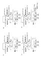
図2に示すように、実施の形態1の撮像装置は、負荷回路100、画素回路110、信号処理回路120を備える。
The output circuit 6 performs conversion necessary for outputting to the outside to the output of the
FIG. 2 is a diagram schematically illustrating a circuit of the imaging apparatus according to the first embodiment.
As shown in FIG. 2, the imaging device of
負荷回路100は、図1の負荷回路2中の1個の回路を記載したものであり、第1信号出力線とGNDとの間に接続された負荷用トランジスタ101を含み、負荷電圧(LG)が供給される。
画素回路110は、図1の撮像部1中の1個の単位セルを記載したものであり、初期化時の電圧を増幅したリセット電圧と読み出し時の電圧を増幅したリード電圧とを第1信号出力線に出力することを特徴とし、入射した光を光電変換し電荷を出力するフォトダイオード等の受光素子111と、受光素子111により発生した電荷を蓄積し、蓄積した電荷を電圧信号として出力するコンデンサ112と、コンデンサ112の示す電圧が初期電圧(ここではVDD)になるようにリセットするリセットトランジスタ113と、受光素子111により出力される電荷をコンデンサ112に供給するリードトランジスタ114と、コンデンサ112の示す電圧に追従して変化する電圧を出力する増幅用トランジスタ115と、行選択エンコーダ3からラインセレクト信号を受けた時に増幅用トランジスタ115の出力を第1信号出力線に出力するラインセレクトトランジスタ116とを含む。ここで本明細書では、以後の説明を容易にする為に、コンデンサ112のうちの、蓄積された電荷に応じた電圧を示す、リセットトランジスタ113、リードトランジスタ114、及び増幅用トランジスタ115が接続している部分を特に電荷検出部117と呼称することとする。
The
The
信号処理回路120は、図1の信号処理部5中の縦1列用の1個の回路を記載したものであり、リード電圧が所定の範囲の電圧である場合に、当該単位セルにより出力されるリセット電圧と当該リード電圧との差分を示す輝度情報を出力し、当該リード電圧が前記所定の範囲の電圧でない場合に、高輝度を示す輝度情報を出力することを特徴とし、第1信号出力線と第2信号出力線との間に直列に接続されたサンプリングトランジスタ121及びクランプ容量122と、第2信号出力線とGNDとの間に直列に接続されたサンプリング容量123と、第2信号出力線と基準電圧端子VDDとの間に直列に接続されたクランプトランジスタ124と、クランプ容量122と並列に接続され、クランプ容量122の端子間にかかる電圧が前記所定の電圧を越えない場合には、この端子間を非導通状態とし、この端子間にかかる電圧が前記所定の電圧を越えた場合には、この端子間を導通状態にするバイパストランジスタ125とを含む。
The
ここで、画素回路110には、リセットパルス(初期化信号:RESET)、リードパルス(読み出しパルス:READ)、及び、ラインセレクトパルス(行選択信号:LSEL)が、信号処理回路120には、サンプリングパルス(SP)、及び、クランプパルス(CP)が決められたタイミングで供給され、これら各制御パルスにそれぞれ対応するトランジスタが開閉(OFF/ON)される。
Here, the
図3は、実施の形態1の撮像装置における各制御パルスのタイミングを示す図である。
図3に示すようなタイミングで各制御パルスを与えることで、ラインセレクトトランジスタ116をONにした状態で、クランプトランジスタ124をONし第2信号出力線を基準電圧にした状態で第1信号出力線にリセット電圧を出力させ(図3のa)、ここでリセット電圧が所定の範囲の電圧であるときには基準電圧とリセット電圧との差分相当がクランプ容量122に保持され(図3のb)、その後、クランプトランジスタ124をOFFにした状態で第1信号出力線にリード電圧を出力させ(図3のc)、ここでリード電圧が所定の範囲の電圧であるときには第2信号出力線の電圧が、当該リセット電圧と当該リード電圧との差分相当だけ当該基準電圧から変化し(図3のd)、これを輝度情報として出力することができ、また、リード電圧が所定の範囲の電圧でないときには、バイパストランジスタ125が端子間を導通状態にすることにより、第2信号出力線の電圧がリード電圧に置き換えられ、これを輝度情報として出力することができる。
FIG. 3 is a diagram illustrating the timing of each control pulse in the imaging apparatus according to the first embodiment.
By giving each control pulse at the timing as shown in FIG. 3, the first signal output line is turned on with the line select transistor 116 turned on, the clamp transistor 124 turned on and the second signal output line is set to the reference voltage. The reset voltage is output (a in FIG. 3), and when the reset voltage is within a predetermined range, the difference between the reference voltage and the reset voltage is held in the clamp capacitor 122 (b in FIG. 3). Then, a read voltage is output to the first signal output line with the clamp transistor 124 turned off (c in FIG. 3). When the read voltage is a voltage within a predetermined range, the voltage of the second signal output line is The difference from the reference voltage is equivalent to the difference between the reset voltage and the read voltage (d in FIG. 3), and this can be output as luminance information. When mode voltage is not the voltage of the predetermined range, by the bypass transistor 125 is between the terminals to the conductive state, the voltage of the second signal output line is replaced by the read voltage can be output as brightness information.
ここで、所定の範囲の電圧の設定方法は、例えばバイパストランジスタ125としてデプレッション型トランジスタを製造時に作り込んでもよいし、電圧供給手段によりバイパストランジスタ125のゲートにバイアス電圧を常時、又は必要なタイミングに(図3のc〜d等)供給してもよい。
例えば、バイパストランジスタ125のゲートにバイアス電圧を、画素回路110からリード電圧を読み出す期間に、パルス状に出力してもよい。
Here, as a method of setting a voltage within a predetermined range, for example, a depletion type transistor may be built as the bypass transistor 125 at the time of manufacture, or a bias voltage is always applied to the gate of the bypass transistor 125 by the voltage supply means or at a necessary timing. (C to d in FIG. 3) may be supplied.
For example, a bias voltage may be output to the gate of the bypass transistor 125 and a pulse may be output during a period in which the read voltage is read from the
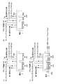
<動作>
図4(a)〜(d)は、画像が暗くなったり画像が黒つぶれする程の強い光を入射していないとき(以下、「通常時」と記す)の各タイミングにおける画素回路110中の領域毎のポテンシャルの状態を示す図である。
ここで図4の各図(a)〜(d)は、それぞれ図3(a)〜(d)のタイミングに対応している。
<Operation>
FIGS. 4A to 4D show the
Here, FIGS. 4A to 4D correspond to the timings of FIGS. 3A to 3D, respectively.
図5(a)は、通常時の、図3(b)のタイミングにおける信号処理回路120中の領域毎のポテンシャルの状態を示す図である。
図5(b)は、通常時の、図3(b’)のタイミングにおける信号処理回路120中の領域毎のポテンシャルの状態を示す図である。
図5(c)は、通常時の、図3(d)のタイミングにおける信号処理回路120中の領域毎のポテンシャルの状態を示す図である。
FIG. 5A is a diagram showing a potential state for each region in the
FIG. 5B is a diagram showing a potential state for each region in the
FIG. 5C is a diagram illustrating a potential state for each region in the
ここで、図4、及び、図5の各図は、上半分が回路の概略を示し、下半分が上半分の回路の各位置に対応する領域毎のポテンシャルの状態を示している。
以下に、通常時の、画素回路110中の領域毎のポテンシャルの遷移、及び、信号処理回路120中の領域毎のポテンシャルの遷移を、図4(a)〜(d)、図5(a)〜(c)に沿って説明する。
Here, in each figure of FIG. 4 and FIG. 5, the upper half shows the outline of the circuit, and the lower half shows the state of the potential for each region corresponding to each position of the upper half circuit.
The potential transition for each region in the
(1)図3(a)のタイミングにおいて、リードトランジスタ114がOFF、リセットトランジスタ113がONなので、図4(a)に示すように、受光素子111で生じた電荷は電荷検出部117には移動せず、電荷検出部117の電荷はVDD端子に移動する。
(2)図3(b)のタイミングにおいて、リセットトランジスタ113がONからOFFになり、図4(b)に示すように、電荷検出部117の電圧がVDDにリセットされ、またクランプトランジスタ124がONなので、図5(a)に示すように、第2信号出力線の電圧がVDDにリセットされる。
(1) Since the read transistor 114 is OFF and the reset transistor 113 is ON at the timing of FIG. 3A, the charge generated in the light receiving element 111 moves to the charge detection unit 117 as shown in FIG. Instead, the charge of the charge detection unit 117 moves to the VDD terminal.
(2) At the timing of FIG. 3B, the reset transistor 113 is turned from ON to OFF, and as shown in FIG. 4B, the voltage of the charge detection unit 117 is reset to VDD, and the clamp transistor 124 is turned on. Therefore, as shown in FIG. 5A, the voltage of the second signal output line is reset to VDD.
(3)図3(b’)のタイミングにおいて、クランプトランジスタ124がONからOFFになり、図5(b)に示すように、リセット電圧とVDDとの差分相当がクランプ容量122に保持される。
(4)図3(c)のタイミングにおいて、リセットトランジスタ113がOFFのまま、リードトランジスタ114がONになるので、図4(c)に示すように、受光素子111で生じた電荷が電荷検出部117に移動する。
(3) At the timing of FIG. 3B ′, the clamp transistor 124 is turned from ON to OFF, and as shown in FIG. 5B, the difference between the reset voltage and VDD is held in the clamp capacitor 122.
(4) At the timing shown in FIG. 3C, the reset transistor 113 remains OFF and the read transistor 114 turns ON. Therefore, as shown in FIG. Move to 117.
(5)図3(d)のタイミングにおいて、図4(d)に示すように、リセットトランジスタ113がOFFのままで、リードトランジスタ114がOFFになるので、受光素子111で生じた電荷が電荷検出部117に読み出される。
ここで、電荷検出部117の電圧が変化し、この変化後の電圧が増幅用トランジスタ115により増幅されるので、第1信号出力線の電圧がリード電圧に変化し、またリセット電圧とVDDとの差分相当がクランプ容量122に保持されているので、図5(c)に示すように、第2信号出力線の電圧が「VDD−第1信号出力線の電圧の変化分相当」となり、この電圧が輝度情報として出力される(第1信号出力線の電圧変化分をSIG、クランプ容量122をCcp、サンプリング容量123をCspとすると:第2信号出力線の電圧はVDD−SIG×Ccp/(Ccp+Csp)となる)。
(5) At the timing of FIG. 3 (d), as shown in FIG. 4 (d), the reset transistor 113 remains OFF and the read transistor 114 is OFF. The data is read by the unit 117.
Here, the voltage of the charge detection unit 117 changes, and the voltage after this change is amplified by the amplifying transistor 115, so that the voltage of the first signal output line changes to the read voltage, and the reset voltage and VDD Since the difference equivalent is held in the clamp capacitor 122, the voltage of the second signal output line becomes “VDD−corresponding to the change in voltage of the first signal output line” as shown in FIG. Is output as luminance information (when the voltage change of the first signal output line is SIG, the clamp capacitor 122 is Ccp, and the sampling capacitor 123 is Csp: the voltage of the second signal output line is VDD−SIG × Ccp / (Ccp + Csp ).
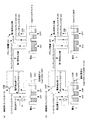
図6(a)〜(d)、及び図7は、画像が暗くなったり画像が黒つぶれする程の強い光を入射したとき(以下、「高輝度時」と記す)の、各タイミングにおける画素回路110中の領域毎のポテンシャルの状態を示す図である。
ここで、図6の各図(a)〜(d)は、それぞれ図3(a)〜(d)のタイミングに対応し、図7は図3(d)において図6(d)の場合よりも強い光を入射したとき、又は図3(d)よりもさらに後のタイミングに対応し、何の対策も施さなければ黒つぶれが生じる状態を示している。
6 (a) to 6 (d) and FIG. 7 show pixels at each timing when light that is strong enough to darken the image or darken the image (hereinafter referred to as "high brightness") is entered. FIG. 3 is a diagram showing a potential state for each region in a
Here, FIGS. 6A to 6D correspond to the timings of FIGS. 3A to 3D, respectively, and FIG. 7 shows the case of FIG. 3 corresponds to the timing when the strong light is incident or later than FIG. 3D, and shows a state where blackout occurs if no measures are taken.
なお、本明細書においては、高輝度時の中でも、図3(b)のタイミングにおいて、第1信号出力線の電荷がバイパストランジスタ125のポテンシャルを越えてしまう程ではない場合を第1高輝度時と記し、第1信号出力線の電荷がバイパストランジスタ125のポテンシャルを越えてしまう程である場合を第2高輝度時と記す。
図8(a)は、第1高輝度時の、図3(b)のタイミングおける信号処理回路120中の領域毎のポテンシャルの状態を示す図である。
In this specification, even when the brightness is high, the case where the charge of the first signal output line does not exceed the potential of the bypass transistor 125 at the timing of FIG. A case where the charge of the first signal output line exceeds the potential of the bypass transistor 125 is referred to as a second high brightness state.
FIG. 8A is a diagram showing a potential state for each region in the
図8(b)は、第1高輝度時の、図3(b’)のタイミングおける信号処理回路120中の領域毎のポテンシャルの状態を示す図である。
図8(c)は、第1高輝度時の、図3(d)のタイミングにおける信号処理回路120中の領域毎のポテンシャルの状態を示す図である。
図9(a)は、第2高輝度時の、図3(b)のタイミングおける信号処理回路120中の領域毎のポテンシャルの状態を示す図である。
FIG. 8B is a diagram illustrating a potential state for each region in the
FIG. 8C is a diagram showing a potential state for each region in the
FIG. 9A is a diagram showing a potential state for each region in the
図9(b)は、第2高輝度時の、図3(b’)のタイミングおける信号処理回路120中の領域毎のポテンシャルの状態を示す図である。
図9(c)は、第2高輝度時の、図3(d)のタイミングにおける信号処理回路120中の領域毎のポテンシャルの状態を示す図である。
ここで、図6、図7、図8、及び、図9の各図は、上半分が回路の概略を示し、下半分が上半分の回路の各位置に対応する領域毎のポテンシャルの状態を示している。
FIG. 9B is a diagram showing a potential state for each region in the
FIG. 9C is a diagram illustrating a potential state for each region in the
6, 7, 8, and 9, the upper half shows the outline of the circuit, and the lower half shows the state of potential for each region corresponding to each position of the upper half circuit. Show.
以下に、高輝度時の、画素回路110中の領域毎のポテンシャルの遷移、及び、信号処理回路120中の領域毎のポテンシャルの遷移を、図6(a)〜(d)、図7、図8(a)〜(c)、及び図9(a)〜(c)に沿って説明する。
(1)図3(a)のタイミングにおいて、リードトランジスタ114がOFF、リセットトランジスタ113がONなので、通常時であれば受光素子111で生じた電荷は電荷検出部117には移動しないが、第1高輝度時及び第2高輝度時では、図6(a)に示すように、受光素子111で生じた電荷はリードトランジスタ114のポテンシャルを越えてしまい電荷検出部117に移動し、同時に電荷検出部117の電荷はVDD端子に移動する。
The potential transition for each region in the
(1) Since the read transistor 114 is OFF and the reset transistor 113 is ON at the timing of FIG. 3A, the charge generated in the light receiving element 111 does not move to the charge detection unit 117 in the normal state. At the time of high luminance and at the time of second high luminance, as shown in FIG. 6A, the charge generated in the light receiving element 111 exceeds the potential of the read transistor 114 and moves to the charge detection unit 117, and at the same time, the charge detection unit. The electric charge 117 moves to the VDD terminal.
(2)図3(b)のタイミングにおいて、リセットトランジスタ113がONからOFFになるが、図6(b)に示すように、引き続き受光素子111で生じた電荷はリードトランジスタ114のポテンシャルを越えて電荷検出部117に移動する為、電荷検出部117の電圧がVDDより低い電圧になってしまう。また、この時クランプトランジスタ124がONなので、第1高輝度時では、図8(a)に示すように、第2信号出力線の電圧がVDDにリセットされ、第1信号出力線の電荷はバイパストランジスタ125のポテンシャルを越えず、第2高輝度時では、図9(a)に示すように、第2信号出力線の電圧がVDDにリセットされるが、同時に、第1信号出力線の電荷がバイパストランジスタ125のポテンシャルを越えてしまい第2信号出力線に移動する。 (2) Although the reset transistor 113 is turned from ON to OFF at the timing of FIG. 3B, the charge generated in the light receiving element 111 continues to exceed the potential of the read transistor 114 as shown in FIG. 6B. Since it moves to the charge detection unit 117, the voltage of the charge detection unit 117 is lower than VDD. Since the clamp transistor 124 is ON at this time, the voltage of the second signal output line is reset to VDD and the charge of the first signal output line is bypassed as shown in FIG. At the time of the second high luminance without exceeding the potential of the transistor 125, as shown in FIG. 9A, the voltage of the second signal output line is reset to VDD, but at the same time, the charge of the first signal output line is reduced. The potential of the bypass transistor 125 is exceeded, and the signal moves to the second signal output line.
(3)図3(b’)のタイミングにおいて、クランプトランジスタ124がONからOFFになり、通常時であれば、第2信号出力線の電圧がVDDにリセットされた状態で、リセット電圧とVDDとの差分がクランプ容量122に保持されるのであるが、第1高輝度時では、図8(b)に示すように、通常時より小さいリセット電圧とVDDとの差分がクランプ容量122に保持され、第2高輝度時では、図9(b)に示すように、第1信号出力線の電荷がバイパストランジスタ125のポテンシャルを越えて第2信号出力線に移動し、クランプ容量122には殆ど電圧の差分は保持されない。 (3) At the timing of FIG. 3B ′, the clamp transistor 124 is turned from ON to OFF, and in the normal state, the voltage of the second signal output line is reset to VDD. Is held in the clamp capacitor 122, but at the time of the first high luminance, as shown in FIG. 8B, the difference between the reset voltage smaller than the normal time and VDD is held in the clamp capacitor 122, At the time of the second high luminance, as shown in FIG. 9B, the charge of the first signal output line moves to the second signal output line beyond the potential of the bypass transistor 125, and almost no voltage is applied to the clamp capacitor 122. Differences are not retained.
なお、図3(b)及び図3(b’)のタイミングにおいて、第2高輝度時に、第1信号出力線の電荷がバイパストランジスタ125のポテンシャルを越えて第2信号出力線に移動し、クランプ容量122には殆ど電圧の差分は保持されないが、このような場合であっても出力結果は同じになるので、以後の動作が重要である。
(4)図3(c)のタイミングにおいて、リセットトランジスタ113がOFFのまま、リードトランジスタ114がONになるので、図6(c)に示すように、受光素子111で生じた電荷が電荷検出部117に移動する。
Note that at the timing of FIGS. 3B and 3B ′, at the second high luminance, the charge of the first signal output line exceeds the potential of the bypass transistor 125 and moves to the second signal output line. Although the voltage difference is hardly held in the capacitor 122, the output result is the same even in such a case, and the subsequent operation is important.
(4) At the timing shown in FIG. 3C, the reset transistor 113 remains OFF and the read transistor 114 turns ON. Therefore, as shown in FIG. Move to 117.
(5)図3(d)のタイミングにおいて、図6(d)に示すように、リセットトランジスタ113がOFFのままで、リードトランジスタ114がOFFになるので、受光素子111で生じた電荷が電荷検出部117に読み出される。
ここで、電荷検出部117の電圧が変化し、この変化後の電圧が増幅用トランジスタ115により増幅されるので、第1信号出力線の電圧がリード電圧に変化し、通常時であれば、リセット電圧とVDDとの差分がクランプ容量122に保持されているので、第2信号出力線の電圧が「VDD−第1信号出力線の電圧の変化分相当」となり、この電圧が輝度情報として出力されるが、第1高輝度時及び第2高輝度時では、それぞれ図8(c)及び図9(c)に示すように、第1信号出力線の電荷がバイパストランジスタ125のポテンシャルを越えて第2信号出力線に移動し、第2信号出力線の電圧が「第1信号出力線の電圧相当」となるので高輝度を示す電圧になり、この電圧が輝度情報として出力される。
(5) At the timing of FIG. 3 (d), as shown in FIG. 6 (d), the reset transistor 113 remains OFF and the read transistor 114 is OFF. The data is read by the unit 117.
Here, the voltage of the charge detection unit 117 is changed, and the voltage after the change is amplified by the amplifying transistor 115. Therefore, the voltage of the first signal output line is changed to the read voltage. Since the difference between the voltage and VDD is held in the clamp capacitor 122, the voltage of the second signal output line becomes “VDD−corresponding to the change in voltage of the first signal output line”, and this voltage is output as luminance information. However, at the time of the first high luminance and the second high luminance, the charge of the first signal output line exceeds the potential of the bypass transistor 125 as shown in FIGS. 8C and 9C, respectively. Since the voltage of the second signal output line becomes “corresponding to the voltage of the first signal output line”, the voltage of the second signal output line becomes a voltage indicating high luminance, and this voltage is output as luminance information.
<まとめ>
図10(a)は、リセット時における第1信号出力線の電圧の特性を示す図である。
図10(b)は、リード時における第1信号出力線の電圧の特性を示す図である。
図10(c)は、画像が暗くなったり画像が黒つぶれすることに対して何の対策も施していない従来の撮像装置における出力電圧の特性を示す図であり、−(図10(a)−図10(b))に相当する。
<Summary>
FIG. 10A is a diagram illustrating the voltage characteristics of the first signal output line at the time of resetting.
FIG. 10B is a diagram illustrating a voltage characteristic of the first signal output line at the time of reading.
FIG. 10C is a diagram illustrating the output voltage characteristics of a conventional imaging device that does not take any measures against dark images or blackened images. -Corresponds to FIG.
図10(d)は、本発明の実施の形態1の撮像装置における出力電圧の特性を示す図であり、所定の電圧を越えた場合には高輝度を示す電圧となるので画像が暗くなったり画像が黒つぶれすることが一切ない。
ここで図10(a)〜(d)において、横軸は入射光の強さ(右が強い)、縦軸は電圧((a),(b)は上がプラス、(c),(d)は上がマイナス)を示す。
FIG. 10D is a diagram showing the characteristics of the output voltage in the imaging apparatus according to
10A to 10D, the horizontal axis indicates the intensity of incident light (right is strong), the vertical axis indicates voltage ((a) and (b) are positive, and (c) and (d). ) Indicates minus on the top.
以上のように、本発明の実施の形態1では、図10(b)に示したリード時の電圧に着目し、リード時の電圧が増幅回路が飽和する辺りの電圧に達した場合に、バイパストランジスタが直接出力電圧を高輝度を示す電圧に置き換えるので、画像が暗くなったり黒つぶれが発生する入射光よりも充分弱い入射光から余裕をもって対策することにより、強い光を入射したときに画像が黒つぶれするという問題点を従来よりも確実に解決し、またリセット時の電圧の変化による悪影響を確実に排除することができる。
(実施の形態2)
<構成>
図11は、実施の形態2の撮像装置の回路の概略を示す図である。
As described above, the first embodiment of the present invention focuses on the voltage at the time of reading shown in FIG. 10B, and bypasses when the voltage at the time of reading reaches a voltage around which the amplifier circuit is saturated. Since the transistor directly replaces the output voltage with a voltage indicating high brightness, the image is displayed when strong light is incident by taking measures with sufficient margin from incident light that is sufficiently weaker than incident light where the image becomes dark or blackout occurs. The problem of black crushing can be solved more reliably than before, and adverse effects due to voltage changes at reset can be reliably eliminated.
(Embodiment 2)
<Configuration>
FIG. 11 is a diagram schematically illustrating a circuit of the imaging apparatus according to the second embodiment.
実施の形態2は、上記実施の形態1の信号処理回路120の代わりに、第2信号出力線が後段の出力アンプの入力ダイナミックレンジを越えた電圧まで変化しないように、第2信号出力線とクリップ電圧端子(CLIPDC)との間に直列に接続したクリップトランジスタ131を追加した信号処理回路130を備える。
実施の形態2の撮像装置は、クリップトランジスタ131を備えることによって、第2信号出力線の電圧が一定電圧以下にならないようにすることができる。
In the second embodiment, instead of the
The image pickup apparatus according to Embodiment 2 includes the clip transistor 131, so that the voltage of the second signal output line can be prevented from becoming a certain voltage or less.
ここで、クリップトランジスタ131の駆動方法として、定電圧で動作させるDC駆動と、適切なタイミングでクリップパルス(CLIP)を与えるパルス駆動とがある。
クリップトランジスタ131をDC駆動させる場合の各制御パルスのタイミングは、実施の形態1の図3と同様である。
またクリップトランジスタ131をパルス駆動させる場合の各制御パルスのタイミングを、以下に説明する。
Here, as a driving method of the clip transistor 131, there are DC driving that operates at a constant voltage and pulse driving that applies a clip pulse (CLIP) at an appropriate timing.
The timing of each control pulse when the clip transistor 131 is DC-driven is the same as that in FIG. 3 of the first embodiment.
The timing of each control pulse when the clip transistor 131 is pulse-driven will be described below.
図12は、実施の形態2の撮像装置におけるクリップトランジスタ131をパルス駆動させる場合のクリップパルスを含む各制御パルスのタイミングを示す図である。
図12に示すように、クリップトランジスタ131をパルス駆動させる場合はサンプリングパルスがOFFになった後にクリップパルスがONとなり(図12のe)、第2信号出力線の電圧が一定電圧以下にならないようにする。ここで図12の(a)〜(d)は図3の(a)〜(d)と同様である。
FIG. 12 is a diagram illustrating the timing of each control pulse including a clip pulse when the clip transistor 131 is pulse-driven in the imaging apparatus according to the second embodiment.
As shown in FIG. 12, when the clip transistor 131 is pulse-driven, the clip pulse is turned on after the sampling pulse is turned off (e in FIG. 12) so that the voltage of the second signal output line does not become a certain voltage or lower. To. Here, (a) to (d) in FIG. 12 are the same as (a) to (d) in FIG.
<動作1>
以下に、クリップトランジスタ131をDC駆動させる場合の動作について説明する。
図13は、高輝度時の図3(d)のタイミングにおける信号処理回路130中の領域毎のポテンシャルの状態を示す図である。
ここで、図13は、上半分が回路の概略を示し、下半分が上半分の回路の各位置に対応する領域毎のポテンシャルの状態を示している。
<
The operation when the clip transistor 131 is DC-driven will be described below.
FIG. 13 is a diagram showing a potential state for each region in the
Here, in FIG. 13, the upper half shows an outline of the circuit, and the lower half shows a potential state for each region corresponding to each position of the upper half circuit.
以下に、高輝度時の、信号処理回路120中の領域毎のポテンシャルの状態を、図13に沿って説明する。
(1)図3(d)のタイミングにおいて、図13に示すように、GNDの電荷が負荷用トランジスタ101のポテンシャルを越えて第1信号出力線に移動し、サンプリングトランジスタ121がONなので、順次電荷が各トランジスタのポテンシャルを越えて移動し、クリップ電圧端子からGNDまでの間に定常電流が流れる。ここで、第2信号出力線の電圧はクリップトランジスタ131のポテンシャルにより定まるので、クリップトランジスタ131のゲート電圧によって定めることができる。
Hereinafter, the state of potential for each region in the
(1) At the timing shown in FIG. 3 (d), as shown in FIG. 13, the GND charge moves over the potential of the load transistor 101 to the first signal output line, and the sampling transistor 121 is ON. Moves beyond the potential of each transistor, and a steady current flows from the clip voltage terminal to GND. Here, since the voltage of the second signal output line is determined by the potential of the clip transistor 131, it can be determined by the gate voltage of the clip transistor 131.
なお、クリップトランジスタ131のポテンシャルは、クリップトランジスタ131としてデプレッション型トランジスタを製造時に作り込むことにより設定してもよい。
ここで、第1信号出力線の電位は、画素回路110内の増幅用トランジスタ115と負荷回路内の負荷用トランジスタ101で構成されているソースフォロワ回路により決まるものであり、GNDと同じ電位になるわけではない。
Note that the potential of the clip transistor 131 may be set by manufacturing a depletion type transistor as the clip transistor 131 at the time of manufacture.
Here, the potential of the first signal output line is determined by the source follower circuit configured by the amplification transistor 115 in the
また、図13からわかるように、クリップトランジスタ131をDC駆動させる場合には、GNDからCLIPDCへ電流が流れるパスが存在するので、消費電力が大きいという問題がある。
<動作2>
以下に、クリップトランジスタ131をパルス駆動させる場合の動作について説明する。
As can be seen from FIG. 13, when the clip transistor 131 is DC-driven, there is a path through which current flows from GND to CLIPDC.
<Operation 2>
The operation when the clip transistor 131 is pulse-driven will be described below.
図14(a)は、高輝度時の図12(d)のタイミングにおける信号処理回路130中の領域毎のポテンシャルの状態を示す図である。
図14(b)は、高輝度時の図12(e)のタイミングにおける信号処理回路130中の領域毎のポテンシャルの状態を示す図である。
ここで、図14(a)(b)は、上半分が回路の概略を示し、下半分が上半分の回路の各位置に対応する領域毎のポテンシャルの状態を示している。
FIG. 14A is a diagram showing a potential state for each region in the
FIG. 14B is a diagram showing a potential state for each region in the
Here, in FIGS. 14A and 14B, the upper half shows an outline of the circuit, and the lower half shows the state of potential for each region corresponding to each position of the upper half circuit.
以下に、高輝度時の、信号処理回路120中の領域毎のポテンシャルの状態を、図14(a)(b)に沿って説明する。
(1)図12(d)のタイミングにおいて、図14(a)に示すように、GNDの電荷が負荷用トランジスタ101のポテンシャルを越えて第1信号出力線に移動し、サンプリングトランジスタ121がON、クリップトランジスタ131がOFFなので、順次電荷が各トランジスタのポテンシャルを越えて第2信号出力線まで移動する。
Below, the state of the potential for each region in the
(1) At the timing shown in FIG. 12 (d), as shown in FIG. 14 (a), the charge on the GND exceeds the potential of the load transistor 101 and moves to the first signal output line, and the sampling transistor 121 is turned on. Since the clip transistor 131 is OFF, the charge sequentially moves to the second signal output line beyond the potential of each transistor.
ここで、第1信号出力線の電位は、画素回路110内の増幅用トランジスタ115と負荷回路内の負荷用トランジスタ101で構成されているソースフォロワ回路により決まるものであり、GNDと同じ電位になるわけではない。
(2)図12(e)のタイミングにおいて、図14(b)に示すように、GNDの電荷が負荷用トランジスタ101のポテンシャルを越えて第1信号出力線に移動し、サンプリングトランジスタ121がOFF、クリップトランジスタ131がONなので、サンプリングトランジスタ121の右側において電荷が各トランジスタのポテンシャルを越えて移動するが、この電荷の移動は、各信号線の電圧が各トランジスタのポテンシャルで決まる電圧に変化した時点で停止する。ここで、第2信号出力線の電圧はクリップトランジスタ131のパルス電圧によって定めることができる。
Here, the potential of the first signal output line is determined by the source follower circuit configured by the amplification transistor 115 in the
(2) At the timing shown in FIG. 12 (e), as shown in FIG. 14 (b), the GND charge exceeds the potential of the load transistor 101 and moves to the first signal output line, and the sampling transistor 121 is turned OFF. Since the clip transistor 131 is ON, the charge moves beyond the potential of each transistor on the right side of the sampling transistor 121. This charge movement occurs when the voltage of each signal line changes to a voltage determined by the potential of each transistor. Stop. Here, the voltage of the second signal output line can be determined by the pulse voltage of the clip transistor 131.
ここで、図14(a)(b)からわかるように、クリップトランジスタ131をパルス駆動させる場合には、GNDからCLIPDCへ電流が流れるパスが存在しないので、クリップトランジスタ131をDC駆動させる場合に較べて消費電力が小さいという利点がある。
<まとめ>
以上のように、本発明の実施の形態2では、実施の形態1の撮像装置に、さらにクリップトランジスタ131を追加したので、第2信号出力線の電圧を、後段の出力アンプの入力ダイナミックレンジを越えた電圧まで変化しないように設定することができる。
(実施の形態3)
<構成>
図15は、実施の形態3の撮像装置の回路の概略を示す図である。
Here, as can be seen from FIGS. 14A and 14B, when the clip transistor 131 is pulse-driven, there is no path through which current flows from GND to CLIPDC, so that the clip transistor 131 is DC-driven. And has the advantage of low power consumption.
<Summary>
As described above, in the second embodiment of the present invention, since the clip transistor 131 is further added to the imaging device of the first embodiment, the voltage of the second signal output line is set to the input dynamic range of the output amplifier in the subsequent stage. It can be set so that it does not change until the voltage exceeds it.
(Embodiment 3)
<Configuration>
FIG. 15 is a diagram schematically illustrating a circuit of the imaging apparatus according to the third embodiment.
図15に示すように、実施の形態3は、実施の形態1の画素回路110の代わりに画素回路140を備え、実施の形態1の信号処理回路120の代わりに信号処理回路150を備える。
画素回路140は、初期化時の電圧を増幅したリセット電圧と読み出し時の電圧を増幅したリード電圧とを第1信号出力線に出力することを特徴とし、入射した光を光電変換して電荷を発生して蓄積し、蓄積した電荷を電圧信号として出力するフォトダイオード等の受光素子141と、受光素子141に蓄積された電荷を掃き出して、ここの電圧が初期電圧(ここではVDD)になるようにリセットするリセットトランジスタ142と、受光素子141に蓄積された電荷による電圧に追従して変化する電圧を出力する増幅用トランジスタ143と、行選択エンコーダ3からラインセレクト信号を受けた時に増幅用トランジスタ143の出力を第1信号出力線に出力するラインセレクトトランジスタ144とを含む。
As shown in FIG. 15, the third embodiment includes a
The
ここで、画素回路140には、リセットパルス(初期化信号:RESET)、及び、ラインセレクトパルス(行選択信号:LSEL)が、信号処理回路120には、サンプリングパルス(SP)、及び、クランプパルス(CP)が決められたタイミングで供給され、これら各制御パルスにそれぞれ対応するトランジスタが開閉(OFF/ON)される。
信号処理回路150は、実施の形態1の信号処理回路120と同様の構成要素を備え、相違点は、実施の形態1の信号処理回路120ではクランプトランジスタ124が第2信号出力線と基準電圧端子VDDとの間に直列に接続されているが、信号処理回路150ではクランプトランジスタ124が第2信号出力線とクランプ用電圧端子VCLとの間に直列に接続されている点のみである。
Here, the
The
ここで、クランプ用電圧端子VCLは、クランプトランジスタ124がONした時に第2信号出力線の電位がバイパストランジスタ125のポテンシャルを越えることのないように、バイパストランジスタ125のポテンシャルを示す電位VφSKIPよりもいくぶん高い電位であり、VCL=VφSKIP+0.1V程度が望ましい。
また、VCLの電位の設定方法は、例えばクランプトランジスタ124としてデプレッション型トランジスタを製造時に作り込んでもよいし、電圧供給手段によりクランプトランジスタ124のゲートにバイアス電圧を常時、又は必要なタイミングに(図16のc〜d等)供給してもよい。
Here, the clamping voltage terminal VCL is somewhat higher than the potential VφSKIP indicating the potential of the bypass transistor 125 so that the potential of the second signal output line does not exceed the potential of the bypass transistor 125 when the clamp transistor 124 is turned on. It is a high potential, and VCL = VφSKIP + 0.1V is desirable.
Further, as a method of setting the potential of VCL, for example, a depletion type transistor may be built as the clamp transistor 124 at the time of manufacturing, or a bias voltage is applied to the gate of the clamp transistor 124 by the voltage supply means at a constant time or at a necessary timing (FIG. C to d, etc.) may be supplied.
例えば、クランプトランジスタ124のゲートにバイアス電圧を、画素回路140からリード電圧を読み出す期間に、パルス状に出力してもよい。
図16は、実施の形態3の撮像装置における各制御パルスのタイミングを示す図である。
図16に示すようなタイミングで各制御パルスを与えることで、ラインセレクトトランジスタ116をONにした状態でクランプトランジスタ124をONして、第1信号出力線にリード電圧を出力させた状態で第2信号出力線を基準電圧にし(図16のa)、ここでリード電圧が所定の範囲の電圧であるときにはリード電圧と基準電圧との差分相当がクランプ容量122に保持され、その後、クランプトランジスタ124をOFFにした状態で(図16のb)第1信号出力線にリセット電圧を出力させ(図16のc)、第2信号出力線の電圧がリセット電圧とリード電圧との差分相当だけ基準電圧から変化し(図16のd)、これを輝度情報として出力することができ、また、リード電圧が所定の範囲の電圧でないときには、バイパストランジスタ125が端子間を導通状態にすることにより、第1信号出力線と第2信号出力線との差分がなくなりクランプ容量122に電荷が保持されないので、その後、第2信号出力線の電圧がリセット電圧に置き換えられ、これを輝度情報として出力することができる。
For example, the bias voltage may be output to the gate of the clamp transistor 124 and the pulse voltage may be output during a period in which the read voltage is read from the
FIG. 16 is a diagram illustrating the timing of each control pulse in the imaging apparatus according to the third embodiment.
By giving each control pulse at the timing as shown in FIG. 16, the clamp transistor 124 is turned on while the line select transistor 116 is turned on, and the second voltage is output while the read voltage is output to the first signal output line. The signal output line is set as a reference voltage (a in FIG. 16). When the read voltage is within a predetermined range, the difference between the read voltage and the reference voltage is held in the clamp capacitor 122, and then the clamp transistor 124 is turned on. In the OFF state (b in FIG. 16), a reset voltage is output to the first signal output line (c in FIG. 16), and the voltage of the second signal output line is changed from the reference voltage by an amount corresponding to the difference between the reset voltage and the read voltage. (D in FIG. 16), this can be output as luminance information, and when the lead voltage is not within a predetermined range, When the register 125 conducts between the terminals, the difference between the first signal output line and the second signal output line disappears, and the charge is not held in the clamp capacitor 122. Thereafter, the voltage of the second signal output line is reset. It is replaced with voltage, and this can be output as luminance information.
ここで、所定の範囲の電圧の設定方法は、例えばバイパストランジスタ125としてデプレッション型トランジスタを製造時に作り込んでもよいし、電圧供給手段によりバイパストランジスタ125のゲートにバイアス電圧を常時、又は必要なタイミングに(図16のc〜d等)供給してもよい。
例えば、バイパストランジスタ125のゲートにバイアス電圧を、画素回路110からリード電圧を読み出す期間に、パルス状に出力してもよい。
Here, as a method of setting a voltage within a predetermined range, for example, a depletion type transistor may be built as the bypass transistor 125 at the time of manufacture, or a bias voltage is always applied to the gate of the bypass transistor 125 by the voltage supply means or at a necessary timing. (C to d in FIG. 16) may be supplied.
For example, a bias voltage may be output to the gate of the bypass transistor 125 and a pulse may be output during a period in which the read voltage is read from the
<動作>
図17(a)〜(d)は、通常時の各タイミングにおける画素回路140中の領域毎のポテンシャルの状態を示す図である。
ここで図17の各図(a)〜(d)は、それぞれ図16(a)〜(d)のタイミングに対応している。
<Operation>
FIGS. 17A to 17D are diagrams illustrating potential states for each region in the
Here, FIGS. 17A to 17D correspond to the timings of FIGS. 16A to 16D, respectively.
図18(a)は、通常時の、図16(a)のタイミングにおける信号処理回路150中の領域毎のポテンシャルの状態を示す図である。
図18(b)は、通常時の、図16(b)のタイミングにおける信号処理回路150中の領域毎のポテンシャルの状態を示す図である。
図18(c)は、通常時の、図16(d)のタイミングにおける信号処理回路150中の領域毎のポテンシャルの状態を示す図である。
FIG. 18A is a diagram illustrating a potential state for each region in the
FIG. 18B is a diagram illustrating a potential state for each region in the
FIG. 18C is a diagram illustrating a potential state for each region in the
ここで、図17、及び、図18の各図は、上半分が回路の概略を示し、下半分が上半分の回路の各位置に対応する領域毎のポテンシャルの状態を示している。
以下に、通常時の、画素回路140中の領域毎のポテンシャルの遷移、及び、信号処理回路150中の領域毎のポテンシャルの遷移を、図17(a)〜(d)、図18(a)〜(c)に沿って説明する。
Here, in each figure of FIG. 17 and FIG. 18, the upper half shows the outline of the circuit, and the lower half shows the state of potential for each region corresponding to each position of the upper half circuit.
The potential transition for each region in the
(1)図16(a)のタイミングにおいて、リセットトランジスタ142がOFFであり、図17(a)に示すように、受光素子141で生じた電荷により受光素子141の電圧が変化し、ラインセレクトトランジスタ144がONなので、この変化後の電圧が増幅用トランジスタ143により増幅され、第1信号出力線の電圧がリード電圧に変化し、また、クランプトランジスタ124がONなので、図18(a)に示すように、第2信号出力線の電圧がVCLにリセットされる。 (1) At the timing of FIG. 16A, the reset transistor 142 is OFF, and as shown in FIG. 17A, the voltage of the light receiving element 141 changes due to the charge generated in the light receiving element 141, and the line select transistor Since 144 is ON, the voltage after this change is amplified by the amplifying transistor 143, the voltage of the first signal output line is changed to the read voltage, and the clamp transistor 124 is ON, so that as shown in FIG. In addition, the voltage of the second signal output line is reset to VCL.
ここでは、バイパストランジスタ125のポテンシャルを示す電位VφSKIPを約0.7V、クランプ用電圧端子VCLを約0.8Vとし、例えば第1信号出力線に出力されたリード電圧を約1.5Vとする。
(2)図16(b)のタイミングにおいて、クランプトランジスタ124がONからOFFになり、図18(b)に示すように、リード電圧とVCLとの差分相当がクランプ容量122に保持される。
Here, the potential VφSKIP indicating the potential of the bypass transistor 125 is about 0.7 V, the clamping voltage terminal VCL is about 0.8 V, and the read voltage output to the first signal output line is about 1.5 V, for example.
(2) At the timing of FIG. 16B, the clamp transistor 124 is turned from ON to OFF, and the difference between the read voltage and VCL is held in the clamp capacitor 122 as shown in FIG.
ここでは、例えばリード電圧約1.5VとVCL約0.8Vとの差分約0.7V相当がクランプ容量122に保持される。
(3)図16(c)のタイミングにおいて、リセットトランジスタ142がONになるので、図17(c)に示すように、受光素子141で生じた電荷はVDD端子に移動する。
Here, for example, a difference equivalent to about 0.7 V between the read voltage of about 1.5 V and the VCL of about 0.8 V is held in the clamp capacitor 122.
(3) Since the reset transistor 142 is turned on at the timing of FIG. 16C, the charge generated in the light receiving element 141 moves to the VDD terminal as shown in FIG.
(4)図16(d)のタイミングにおいて、リセットトランジスタ142がONからOFFになり、図17(d)に示すように、受光素子141の電圧がVDDにリセットされる。
ここで、受光素子141の電圧がVDDに変化し、この変化後の電圧が増幅用トランジスタ115により増幅されるので、第1信号出力線の電圧がリセット電圧に変化し、またリード電圧とVCLとの差分相当がクランプ容量122に保持されているので、図16(c)に示すように、第2信号出力線の電圧が「VCL+第1信号出力線の電圧の変化分相当」となり、この電圧が輝度情報として出力される(第1信号出力線の電圧変化分をSIG、クランプ容量122をCcp、サンプリング容量123をCspとすると:第2信号出力線の電圧はVCL+SIG×Ccp/(Ccp+Csp)となる)。
(4) At the timing of FIG. 16D, the reset transistor 142 is turned from ON to OFF, and as shown in FIG. 17D, the voltage of the light receiving element 141 is reset to VDD.
Here, the voltage of the light receiving element 141 changes to VDD, and the voltage after this change is amplified by the amplifying transistor 115, so that the voltage of the first signal output line changes to the reset voltage, and the read voltage, VCL, 16 is held in the clamp capacitor 122, the voltage of the second signal output line becomes “VCL + corresponding to the change in the voltage of the first signal output line” as shown in FIG. Is output as luminance information (when the voltage change of the first signal output line is SIG, the clamp capacitor 122 is Ccp, and the sampling capacitor 123 is Csp: the voltage of the second signal output line is VCL + SIG × Ccp / (Ccp + Csp) Become).
ここでは、例えば第1信号出力線に出力されたリセット電圧Vresetを約2.0Vとし、Ccp=Cspとすると、第2信号出力線の電圧Vnrmは、Vnrm=VCL+SIG×Ccp/(Ccp+Csp)=0.8+(2.0−1.5)×(1/2)=1.05(V)となる。
図19(a)〜(d)は、高輝度時の、各タイミングにおける画素回路140中の領域毎のポテンシャルの状態を示す図である。
Here, for example, when the reset voltage Vreset output to the first signal output line is about 2.0 V and Ccp = Csp, the voltage Vnrm of the second signal output line is Vnrm = VCL + SIG × Ccp / (Ccp + Csp) = 0. .8+ (2.0−1.5) × (1/2) = 1.05 (V).
FIGS. 19A to 19D are diagrams showing potential states for each region in the
ここで、図19の各図(a)〜(d)は、それぞれ図16(a)〜(d)のタイミングに対応している。
図20(a)は、高輝度時の、図16(a)のタイミングおける信号処理回路150中の領域毎のポテンシャルの状態を示す図である。
図20(b)は、通常時の、図16(b)のタイミングにおける信号処理回路150中の領域毎のポテンシャルの状態を示す図である。
Here, each of FIGS. 19A to 19D corresponds to the timings of FIGS. 16A to 16D, respectively.
FIG. 20A is a diagram illustrating a potential state for each region in the
FIG. 20B is a diagram showing a potential state of each region in the
図20(c)は、通常時の、図16(d)のタイミングにおける信号処理回路150中の領域毎のポテンシャルの状態を示す図である。
ここで、図19、及び、図20の各図は、上半分が回路の概略を示し、下半分が上半分の回路の各位置に対応する領域毎のポテンシャルの状態を示している。
以下に、高輝度時の、画素回路140中の領域毎のポテンシャルの遷移、及び、信号処理回路150中の領域毎のポテンシャルの遷移を、図19(a)〜(d)、図20(a)〜(c)に沿って説明する。
FIG. 20C is a diagram illustrating a potential state of each region in the
Here, in each figure of FIG. 19 and FIG. 20, the upper half shows the outline of the circuit, and the lower half shows the state of potential for each region corresponding to each position of the upper half circuit.
The potential transition for each region in the
(1)図16(a)のタイミングにおいて、リセットトランジスタ142がOFFであり、図19(a)に示すように、受光素子141で生じた電荷により受光素子141の電圧が変化し、ラインセレクトトランジスタ144がONなので、この変化後の電圧が増幅用トランジスタ143により増幅され、第1信号出力線の電圧がリード電圧に変化し、また、クランプトランジスタ124がONなので、第2信号出力線の電圧がVCLにリセットされる。 (1) At the timing of FIG. 16A, the reset transistor 142 is OFF, and as shown in FIG. 19A, the voltage of the light receiving element 141 changes due to the charge generated in the light receiving element 141, and the line select transistor Since 144 is ON, the voltage after the change is amplified by the amplifying transistor 143, the voltage of the first signal output line is changed to a read voltage, and since the clamp transistor 124 is ON, the voltage of the second signal output line is Reset to VCL.
ここでは、バイパストランジスタ125のポテンシャルを示す電位VφSKIPを約0.7V、クランプ用電圧端子VCLを約0.8Vとし、例えば第1信号出力線に出力されたリード電圧を約0.5Vとする。
(2)図16(b)のタイミングにおいて、クランプトランジスタ124がONからOFFになり、ここで、通常時であればリード電圧と基準電圧との差分相当がクランプ容量122に保持されるが、高輝度時では、図20(b)に示すように、リード電圧のポテンシャルがバイパストランジスタ125のポテンシャルを越えてしまいバイパストランジスタ125が端子間を導通状態にするので、クランプ容量122に電荷が保持されない。
Here, the potential VφSKIP indicating the potential of the bypass transistor 125 is about 0.7 V, the clamping voltage terminal VCL is about 0.8 V, and the read voltage output to the first signal output line is about 0.5 V, for example.
(2) At the timing of FIG. 16 (b), the clamp transistor 124 is turned from ON to OFF. Here, in a normal time, the difference between the read voltage and the reference voltage is held in the clamp capacitor 122. At the time of luminance, as shown in FIG. 20B, the potential of the read voltage exceeds the potential of the bypass transistor 125, and the bypass transistor 125 conducts between the terminals, so that no charge is held in the clamp capacitor 122.
ここでは、例えばリード電圧約0.5Vが、VφSKIP約0.7V越えてしまうので、第1信号出力線及び第2信号出力線の電圧は共に約0.5Vとなり、クランプ容量122に電荷が保持されない。
(3)図16(c)のタイミングにおいて、リセットトランジスタ142がONになるので、図19(c)に示すように、受光素子141で生じた電荷はVDD端子に移動する。
Here, for example, since the read voltage of about 0.5 V exceeds VφSKIP of about 0.7 V, the voltages of the first signal output line and the second signal output line are both about 0.5 V, and the charge is held in the clamp capacitor 122. Not.
(3) Since the reset transistor 142 is turned on at the timing shown in FIG. 16C, the charge generated in the light receiving element 141 moves to the VDD terminal as shown in FIG. 19C.
(4)図16(d)のタイミングにおいて、リセットトランジスタ142がONからOFFになるが、図19(d)に示すように、受光素子141からは、高輝度光入射で生じた電荷により、VDDよりも若干低い電圧が出力される。
ここで、クランプ容量122には電荷が保持されていないので、図20(c)に示すように、第2信号出力線の電圧がリセット電圧に相当する電圧となるので高輝度を示す電圧になり、この電圧が輝度情報として出力される。
(4) At the timing of FIG. 16D, the reset transistor 142 is turned from ON to OFF, but as shown in FIG. 19D, the light receiving element 141 receives VDD from the high-intensity light incident. A slightly lower voltage is output.
Here, since no electric charge is held in the clamp capacitor 122, the voltage of the second signal output line becomes a voltage corresponding to the reset voltage as shown in FIG. This voltage is output as luminance information.
具体的には、第1信号出力線の電圧がバイパストランジスタのポテンシャルを超えている間は、第1信号出力線の電圧=第2信号出力線の電圧となるが、第1信号出力線の電圧がバイパストランジスタのポテンシャルよりも高い電圧になると、第2信号出力線の電圧は、第1信号出力線の電圧変動に対し、サンプリング容量Csp、クランプ容量Ccpで定まる一定の比で変化し、この時の第2信号出力線の電圧Vovは、下式で表される。 Specifically, while the voltage of the first signal output line exceeds the potential of the bypass transistor, the voltage of the first signal output line = the voltage of the second signal output line. Becomes a voltage higher than the potential of the bypass transistor, the voltage of the second signal output line changes with a constant ratio determined by the sampling capacitor Csp and the clamp capacitor Ccp with respect to the voltage fluctuation of the first signal output line. The voltage Vov of the second signal output line is expressed by the following equation.
Vov=VφSKIP+(Vreset−VφSKIP)
×Ccp/(Ccp+Csp)
ここでは、例えば第1信号出力線に出力されたリセット電圧Vresetを約1.9Vとし、Ccp=Cspとすると、第2信号出力線の電圧Vovは、Vov=VφSKIP+(Vreset−VφSKIP)×Ccp/(Ccp+Csp)=0.7+(1.9−0.7)×(1/2)=1.3(V)となる。
Vov = VφSKIP + (Vreset−VφSKIP)
× Ccp / (Ccp + Csp)
Here, for example, when the reset voltage Vreset output to the first signal output line is about 1.9 V and Ccp = Csp, the voltage Vov of the second signal output line is Vov = VφSKIP + (Vreset−VφSKIP) × Ccp / (Ccp + Csp) = 0.7 + (1.9−0.7) × (1/2) = 1.3 (V).
上記の例によればVov>Vnrmが成り立つ。
但し、VCL≫VφSKIPとするとVov>Vnrmが成り立たなくなるので、VCLとVφSKIPとの差は、上記のようにVov>Vnrmが成り立たつ範囲に限られ、例えば、VCL=約0.8V、VφSKIP=約0.7Vであり、その差は0.1V程度が適当である。
According to the above example, Vov> Vnrm holds.
However, when VCL >> VφSKIP, Vov> Vnrm does not hold, so the difference between VCL and VφSKIP is limited to the range where Vov> Vnrm holds as described above. For example, VCL = about 0.8 V, VφSKIP = about It is 0.7V, and the difference is suitably about 0.1V.
<まとめ>
本発明の実施の形態3の撮像装置における出力電圧の特性は、実施の形態1と同様であり、リード電圧が所定の電圧を越えた場合には高輝度を示す電圧となるので画像が暗くなったり画像が黒つぶれすることがなく、実施の形態1と同様の効果を得ることができる。
(変形例1)
図21(a)(b)は、リセットトランジスタのポテンシャルと、バイパストランジスタのポテンシャルの関係を示す図である。
<Summary>
The characteristics of the output voltage in the imaging apparatus according to the third embodiment of the present invention are the same as those in the first embodiment. When the read voltage exceeds a predetermined voltage, the voltage becomes high and the image becomes dark. In other words, the same effect as in the first embodiment can be obtained.
(Modification 1)
FIGS. 21A and 21B are diagrams showing the relationship between the potential of the reset transistor and the potential of the bypass transistor.
以下に図21(a)(b)を用いて、リセットトランジスタのポテンシャルを示す電位VφRと、バイパストランジスタのポテンシャルを示す電位VφSKIPとの関係を説明する。
ここで増幅用トランジスタの増幅率をα、閾値電圧をVtとする。
図21(a)に示すように、VφSKIPが、VφRで決まる第1信号出力線の最小電位“Vmin=(VφR−Vt)×α”以下に設定した場合(VφSKIP/α+Vt≦VφR)には、飽和信号分が“Vsat=VDD−VφR”となり実質的な飽和出力電位を最大限に確保できるが、高輝度時においてバイパストランジスタがONしないので、バイパストランジスタとして機能しない。
Hereinafter, the relationship between the potential VφR indicating the potential of the reset transistor and the potential VφSKIP indicating the potential of the bypass transistor will be described with reference to FIGS.
Here, the amplification factor of the amplifying transistor is α, and the threshold voltage is Vt.
As shown in FIG. 21A, when VφSKIP is set below the minimum potential “Vmin = (VφR−Vt) × α” of the first signal output line determined by VφR (VφSKIP / α + Vt ≦ VφR), The saturation signal component is “Vsat = VDD−VφR”, and a substantial saturation output potential can be secured to the maximum. However, since the bypass transistor is not turned on at high luminance, it does not function as a bypass transistor.
図21(b)に示すように、VφSKIPが、VφRで決まる第1信号出力線の最小電位“Vmin=(VφR−Vt)×α”よりも高く設定した場合VφSKIP/α+Vt>VφR)には、飽和信号分が“Vsat=VDD−(VφSKIP/α+Vt)”となり、VφSKIPとVminとの差分がある程度以上大きければバイパストランジスタとして機能するが、この差分が大きい程より実質的な飽和出力電位が低下する。 As shown in FIG. 21B, when VφSKIP is set higher than the minimum potential “Vmin = (VφR−Vt) × α” of the first signal output line determined by VφR, VφSKIP / α + Vt> VφR) The saturation signal becomes “Vsat = VDD− (VφSKIP / α + Vt)”, and functions as a bypass transistor if the difference between VφSKIP and Vmin is larger than a certain level. However, the larger this difference is, the lower the substantial saturation output potential is. .
ここでVφSKIPとVminとの差分は0.1V程度が望ましい。
なお、バイパストランジスタとリセットトランジスタとを同一の工程で生産し、バイパストランジスタのゲートにバイアス電圧を供給し、ここで、バイパストランジスタのポテンシャルを示す電位と飽和信号出力電位との差分は、バイアス電圧によって与えてもよい。
Here, the difference between VφSKIP and Vmin is preferably about 0.1V.
The bypass transistor and the reset transistor are produced in the same process, and a bias voltage is supplied to the gate of the bypass transistor. Here, the difference between the potential indicating the potential of the bypass transistor and the saturation signal output potential depends on the bias voltage. May be given.
また、リセットトランジスタは所定の埋め込み注入によって生産され、バイパストランジスタは当該所定の埋め込み注入に加え、追加注入を経て生産し、ここで、バイパストランジスタのポテンシャルを示す電位と飽和信号出力電位との差分は追加注入によって与えてもよい。
<まとめ>
以上のように、本発明の変形例1によれば、実質的な飽和出力電圧を十分に確保し、かつ、バイパストランジスタとして機能するのでその効果が期待できる。
(変形例2)
撮像装置には、1フレーム毎に所定数の画素分の輝度情報が撮像部から出力されない垂直ブランキング期間がある。
The reset transistor is produced by a predetermined implantation, and the bypass transistor is produced through an additional implantation in addition to the predetermined implantation. Here, the difference between the potential indicating the potential of the bypass transistor and the saturation signal output potential is May be given by additional injection.
<Summary>
As described above, according to
(Modification 2)
The imaging apparatus has a vertical blanking period in which luminance information for a predetermined number of pixels is not output from the imaging unit for each frame.
垂直ブランキング期間において通常の期間と同様に駆動すると、負荷回路により第1信号出力線の電位は0Vになり過度の飽和出力信号が出ていることになるので、後段の出力アンプの入力ダイナミックレンジが制約を受け、微少な信号を十分にゲインアップできないという問題が生じる。
そこで本発明の変形例2は、このような問題を解決する為に、垂直ブランキング期間において飽和出力信号を出さない撮像装置、及び撮像方法等を提供する。
When the vertical blanking period is driven in the same manner as in the normal period, the load circuit causes the potential of the first signal output line to be 0 V and an excessive saturation output signal is output, so the input dynamic range of the output amplifier in the subsequent stage However, there is a problem that the gain of a minute signal cannot be sufficiently increased.
Therefore, in order to solve such a problem, the second modification of the present invention provides an imaging apparatus, an imaging method, and the like that do not output a saturated output signal in the vertical blanking period.
図22は、変形例2におけるサンプリングパルスのタイミングを示す図である。
ここで図22に示すサンプリングパルスは、実施の形態1と同様の撮像装置に対して出力される例を示しており、列選択エンコーダ4に含まれるサンプリングトランジスタ制御部により出力されるものとする。
図22に示すように、垂直ブランキング期間においては、サンプリングトランジスタ制御部がサンプリングパルスを出力しないので、サンプリングトランジスタ121が非導通状態となり、クランプ容量122に電荷は一切保持されず、結果的に低輝度を示す輝度情報が出力されることになる。
FIG. 22 is a diagram illustrating the timing of sampling pulses in the second modification.
Here, the sampling pulse shown in FIG. 22 shows an example of being output to the same imaging apparatus as in the first embodiment, and is output by the sampling transistor control unit included in the column selection encoder 4.
As shown in FIG. 22, in the vertical blanking period, since the sampling transistor control unit does not output a sampling pulse, the sampling transistor 121 becomes non-conductive, and no charge is held in the clamp capacitor 122, resulting in a low level. Luminance information indicating the luminance is output.
<まとめ>
以上のように、本発明の変形例2によれば、垂直ブランキング期間において飽和出力信号は出ないので、後段の出力アンプの入力ダイナミックレンジが制約を受けない。
(変形例3)
本発明の変形例3は、変形例2と同様の問題を解決する為に、垂直ブランキング期間において飽和出力信号を出さない撮像装置、及び撮像方法等を提供する。
<Summary>
As described above, according to the second modification of the present invention, since a saturated output signal is not output during the vertical blanking period, the input dynamic range of the output amplifier at the subsequent stage is not restricted.
(Modification 3)
図23は、変形例3における負荷用トランジスタの制御のタイミングを示す図である。
ここで図23に示す負荷用トランジスタのゲート電圧の制御は、実施の形態1と同様の撮像装置に対して行われる例を示しており、列選択エンコーダ4に含まれる負荷用トランジスタ制御部により行われるものとする。
図23に示すように、垂直ブランキング期間においては、負荷用トランジスタ制御部が負荷用トランジスタにバイアス電圧を印加しないので、負荷用トランジスタ101が非導通状態となり、クランプ容量122に電荷は一切保持されず、結果的に低輝度を示す輝度情報が出力されることになる。
FIG. 23 is a diagram illustrating the control timing of the load transistor in the third modification.
Here, the control of the gate voltage of the load transistor shown in FIG. 23 is an example performed for the same image pickup apparatus as that in the first embodiment, and is performed by the load transistor control unit included in the column selection encoder 4. Shall be.
As shown in FIG. 23, in the vertical blanking period, the load transistor control unit does not apply a bias voltage to the load transistor, so that the load transistor 101 becomes non-conductive and no charge is held in the clamp capacitor 122. As a result, luminance information indicating low luminance is output.
<まとめ>
以上のように、本発明の変形例3によれば、垂直ブランキング期間において飽和出力信号は出ないので、後段の出力アンプの入力ダイナミックレンジが制約を受けない。
なお、本発明で説明に用いた各回路は、単に一例を示すものであって、同様の機能を備えた他の回路等であってもよい。
<Summary>
As described above, according to the third modification of the present invention, since a saturated output signal is not output in the vertical blanking period, the input dynamic range of the output amplifier at the subsequent stage is not restricted.
Note that each circuit used in the description of the present invention is merely an example, and may be another circuit or the like having a similar function.
また、各信号処理回路の代わりに、リセット電圧とリード電圧とをそれぞれ別途計測し、これら計測結果に基づき、汎用のプロセッサにより各信号処理回路と同様の処理を実現するものであってもよいし、また通常時は従来の信号処理回路により動作し、汎用のプロセッサによりリード時の電圧が所定の範囲の電圧でないときにのみ高輝度時であると判断して、この時の出力信号を高輝度を示す輝度情報に置き換えてもよい。 Further, instead of each signal processing circuit, the reset voltage and the read voltage may be separately measured, and based on these measurement results, the same processing as each signal processing circuit may be realized by a general-purpose processor. Also, it operates normally with a conventional signal processing circuit, and a general-purpose processor determines that the brightness is high only when the read voltage is not within a predetermined range, and the output signal at this time is It may be replaced with luminance information indicating.
また、クランプトランジスタやバイパストランジスタ等の各ゲートに、電圧供給手段により供給される各バイアス電圧を、個々の撮像装置毎に適正な値に設定する為に、電圧供給手段は内部に各バイアス電圧を外部より設定可能であり設定された値を記憶できるバイアス電圧設定回路を含んでもよい。
このバイアス電圧設定回路は、バイアス電圧を供給すべきトランジスタ毎に、例えば外部より特定の端子に所定の電圧をかけることによって切断可能なポリシリコン等の配線が複数並列に接続され、複数の配線のそれぞれには同一又は異なる抵抗等の電圧を変化させることができる素子を備えており、製造工程の最終段階において、接続されたトランジスタのポテンシャルが最適な値になるように、出力データをモニターしながら複数の配線の何れかを切断する。例えば、バイパストランジスタのポテンシャルを示す電位と飽和信号出力電位との差分が最適な値になるように、第2信号出力線の電圧をモニターしながら複数の配線の何れかを切断することによって、バイパストランジスタのバイアス電圧を設定する。
In addition, in order to set each bias voltage supplied by the voltage supply means to each gate such as a clamp transistor and a bypass transistor to an appropriate value for each imaging device, the voltage supply means internally sets each bias voltage. A bias voltage setting circuit that can be set from the outside and can store the set value may be included.
In this bias voltage setting circuit, for each transistor to which a bias voltage is to be supplied, a plurality of wirings such as polysilicon that can be cut by applying a predetermined voltage to a specific terminal from the outside are connected in parallel. Each is equipped with an element that can change the voltage, such as the same or different resistance, while monitoring the output data so that the potential of the connected transistor becomes the optimum value at the final stage of the manufacturing process. Cut any of the plurality of wires. For example, by bypassing any of the plurality of wirings while monitoring the voltage of the second signal output line so that the difference between the potential indicating the potential of the bypass transistor and the saturation signal output potential becomes an optimum value. Sets the transistor bias voltage.
また、本発明の各実施の形態及び各変形例においては、信号電荷が電子の場合を例にとり説明したが、信号電荷を正孔としても実現可能である。信号電荷が正孔の場合には、信号電荷が電子の場合と比較して、信号極性が反転し、電位の大小関係が逆になるだけである。
また、本発明の各実施の形態及び各変形例においては、MOS型増幅トランジスタを例にとり説明したが、CMD、BASIS、SIT等のFPN除去回路を必要とする撮像装置であっても実現可能である。
In each embodiment and each modification of the present invention, the case where the signal charge is an electron has been described as an example. However, the signal charge can be realized as a hole. When the signal charge is a hole, the signal polarity is reversed and the potential relationship is only reversed as compared with the case where the signal charge is an electron.
In each embodiment and each modification of the present invention, a MOS type amplification transistor has been described as an example. However, an imaging apparatus that requires an FPN removal circuit such as CMD, BASIS, or SIT can also be realized. is there.
本発明は、家庭用ビデオカメラやデジタルスチルカメラなどの撮像機器に適用することができる。本発明によって、強い光を入射したときに画像が黒つぶれするという問題点を従来よりも確実に解決し、またリセット時の電圧の変化による悪影響を確実に排除することができる固体撮像素子が提供でき、撮像機器の画質の向上に寄与することができる。
また、家庭用だけでなく、あらゆる撮像機器に適用することができる。
The present invention can be applied to imaging devices such as home video cameras and digital still cameras. According to the present invention, there is provided a solid-state imaging device that can reliably solve the problem that an image is blacked out when strong light is incident, and can reliably eliminate the adverse effects caused by a voltage change at reset. This can contribute to the improvement of the image quality of the imaging device.
Further, it can be applied not only to home use but also to any imaging device.
図5(b)は、通常時の、図3(b’)のタイミングにおける信号処理回路120中の領域毎のポテンシャルの状態を示す図である。
図5(c)は、通常時の、図3(d)のタイミングにおける信号処理回路120中の領域毎のポテンシャルの状態を示す図である。
FIG. 5C is a diagram illustrating a potential state for each region in the
図8(b)は、第1高輝度時の、図3(b’)のタイミングおける信号処理回路120中の領域毎のポテンシャルの状態を示す図である。
図8(c)は、第1高輝度時の、図3(d)のタイミングにおける信号処理回路120中の領域毎のポテンシャルの状態を示す図である。
FIG. 8C is a diagram showing a potential state for each region in the
図9(b)は、第2高輝度時の、図3(b’)のタイミングおける信号処理回路120中の領域毎のポテンシャルの状態を示す図である。
図9(c)は、第2高輝度時の、図3(d)のタイミングにおける信号処理回路120中の領域毎のポテンシャルの状態を示す図である。
FIG. 9C is a diagram illustrating a potential state for each region in the
図10(b)は、リード時における第1信号出力線の電圧の特性を示す図である。
図10(c)は、画像が暗くなったり画像が黒つぶれすることに対して何の対策も施していない従来の撮像装置における出力電圧の特性を示す図であり、−(図10(a)−図10(b))に相当する。
図10(d)は、本発明の実施の形態1の撮像装置における出力電圧の特性を示す図である。
FIG. 10C is a diagram illustrating the output voltage characteristics of a conventional imaging device that does not take any measures against dark images or blackened images. -Corresponds to FIG.
FIG. 10D is a diagram showing the output voltage characteristics in the imaging apparatus according to
図14(b)は、高輝度時の図12(e)のタイミングにおける信号処理回路130中の領域毎のポテンシャルの状態を示す図である。
図18(b)は、通常時の、図16(b)のタイミングにおける信号処理回路150中の領域毎のポテンシャルの状態を示す図である。
図18(c)は、通常時の、図16(d)のタイミングにおける信号処理回路150中の領域毎のポテンシャルの状態を示す図である。
FIG. 18C is a diagram illustrating a potential state for each region in the
図20(a)は、高輝度時の、図16(a)のタイミングおける信号処理回路150中の領域毎のポテンシャルの状態を示す図である。
図20(c)は、通常時の、図16(d)のタイミングにおける信号処理回路150中の領域毎のポテンシャルの状態を示す図である。
1 撮像部
2 負荷回路
3 行選択エンコーダ
4 列選択エンコーダ
5 信号処理部
6 出力回路
100 負荷回路
101 負荷用トランジスタ
110 画素回路
111 受光素子
112 コンデンサ
113 リセットトランジスタ
114 リードトランジスタ
115 増幅用トランジスタ
116 ラインセレクトトランジスタ
117 電荷検出部
120 信号処理回路
121 サンプリングトランジスタ
122 クランプ容量
123 サンプリング容量
124 クランプトランジスタ
125 バイパストランジスタ
130 信号処理回路
131 クリップトランジスタ
140 画素回路
141 受光素子
142 リセットトランジスタ
143 増幅用トランジスタ
144 ラインセレクトトランジスタ
150 信号処理回路
DESCRIPTION OF
Claims (15)
前記単位セル毎に、受光量に応じた電圧情報を出力する出力手段とを備える撮像装置であって、
前記出力手段は、
前記撮像手段に接続され、前記リード電圧及び前記リセット電圧を受け付ける信号出力線と、
前記信号出力線に接続されたクランプ容量と、
ゲート電位を固定電位とし、前記リード電圧が所定の範囲の電圧である場合には前記クランプ容量の端子間を非導通状態とし、前記リード電圧が所定の範囲の電圧でない場合には当該端子間を導通状態とする第1のトランジスタを含むこと
を特徴とする撮像装置。 The unit cell that outputs the reset voltage corresponding to the output voltage of the photoelectric conversion unit when the photoelectric conversion unit is the initial voltage and the read voltage corresponding to the output voltage of the photoelectric conversion unit according to the amount of received light is one-dimensional, Or a plurality of imaging means arranged two-dimensionally;
An output device that outputs voltage information corresponding to the amount of received light for each unit cell,
The output means includes
A signal output line connected to the imaging means for receiving the read voltage and the reset voltage;
A clamp capacitor connected to the signal output line;
The gate potential to a fixed potential, when the read voltage is a voltage of a predetermined range, the non-conductive state between the terminals of the clamp capacitance, between the corresponding pin when the read voltage is not a voltage of a predetermined range An imaging device comprising: a first transistor that is in a conductive state.
を特徴とする請求項1に記載の撮像装置。 The case where the voltage is within the predetermined range is a case where the potential of the signal output line is higher than the potential indicating the potential of the first transistor, and the case where the voltage is not within the predetermined range. The imaging apparatus according to claim 1, wherein the potential of the output line is equal to or lower than the potential indicating the potential of the first transistor.
前記第1のトランジスタのゲートに、バイアス電圧を供給する電圧供給手段を含むこと
を特徴とする請求項1に記載の撮像装置。 The output means further includes:
The imaging apparatus according to claim 1, further comprising voltage supply means for supplying a bias voltage to the gate of the first transistor.
を特徴とする請求項1に記載の撮像装置。 The imaging device according to claim 1, wherein the first transistor is a depletion type transistor.
受光量に応じた電荷を発生する受光素子と、
受光素子により発生した電荷を保持し、電圧信号として出力する電荷検出部と、
リセット用基準電圧端子と前記電荷検出部との間に接続され、ゲート電圧が印加されて導通状態であるときに、前記電荷検出部が基準電圧にリセットされるリセットトランジスタと、
増幅用基準電圧端子と前記信号出力線との間に接続され、前記電荷検出部により変換された電圧信号がゲートに印加され、当該電圧信号を増幅して前記信号出力線へ出力する増幅用トランジスタとを含み、
前記第1のトランジスタのポテンシャルを示す電位は、前記リセットトランジスタが非導通状態であるときのリセットトランジスタの電位に依存する当該単位セルに含まれる前記増幅用トランジスタの出力である飽和信号出力電位よりも、所定の差分だけ高いこと
を特徴とする請求項1に記載の撮像装置。 Each unit cell in the imaging means is
A light receiving element that generates a charge corresponding to the amount of light received;
A charge detector that holds the charge generated by the light receiving element and outputs it as a voltage signal;
A reset transistor connected between a reference voltage terminal for reset and the charge detection unit, wherein the charge detection unit is reset to a reference voltage when a gate voltage is applied and is in a conductive state;
An amplifying transistor that is connected between an amplifying reference voltage terminal and the signal output line, applies a voltage signal converted by the charge detector to the gate, amplifies the voltage signal, and outputs the amplified voltage signal to the signal output line Including
The potential indicating the potential of the first transistor is higher than a saturation signal output potential that is an output of the amplifying transistor included in the unit cell depending on the potential of the reset transistor when the reset transistor is in a non-conductive state. The imaging apparatus according to claim 1, wherein the imaging apparatus is higher by a predetermined difference.
を特徴とする請求項5に記載の撮像装置。 The imaging apparatus according to claim 5, wherein a difference between a potential indicating the potential of the first transistor and the saturation signal output potential is approximately 0.1V.
前記第1のトランジスタのゲートに、バイアス電圧を供給する電圧供給手段を含み、
前記第1のトランジスタのポテンシャルを示す電位と前記飽和信号出力電位との差分は、前記バイアス電圧によって与えられること
を特徴とする請求項5に記載の撮像装置。 The output means further includes:
Voltage supply means for supplying a bias voltage to the gate of the first transistor;
The imaging device according to claim 5, wherein a difference between a potential indicating the potential of the first transistor and the saturation signal output potential is given by the bias voltage.
を特徴とする請求項5に記載の撮像装置。 The imaging device according to claim 5, wherein the first transistor and the reset transistor are produced in the same process.
撮像装置毎に異なる適切なバイアス電圧を、外部より設定することができるバイアス電圧設定回路を含むこと
を特徴とする請求項7に記載の撮像装置。 The voltage supply means includes
The image pickup apparatus according to claim 7, further comprising a bias voltage setting circuit capable of setting an appropriate bias voltage that is different for each image pickup apparatus from outside.
前記第1のトランジスタは、前記所定の埋め込み注入に加え、追加注入を経て生産され、
前記第1のトランジスタのポテンシャルを示す電位と前記飽和信号出力電位との差分は、前記追加注入によって与えられること
を特徴とする請求項5に記載の撮像装置。 The reset transistor is produced by a predetermined implantation implantation,
The first transistor is produced through an additional implantation in addition to the predetermined implantation implantation,
The imaging apparatus according to claim 5, wherein the difference between the potential indicating the potential of the first transistor and the saturation signal output potential is given by the additional injection.
前記単位セル毎に、受光量に応じた電圧情報を出力する出力手段とを備える撮像装置であって、
前記出力手段は、
前記撮像手段に接続され、前記リード電圧及び前記リセット電圧を受け付ける第1信号出力線と、
前記電圧情報を出力する第2信号出力線と、
前記第1信号出力線と前記第2信号出力線との間に直列に接続されているクランプ容量と、
前記クランプ容量と並列に接続され、ソース電極が前記第1信号出力線に接続し、ドレイン電極が前記第2信号出力線に接続したゲート電位が固定電位となる第1のトランジスタを含み、当該第1のトランジスタは、前記リード電圧が所定の範囲の電圧である場合には、前記クランプ容量の端子間を非導通状態とし、前記リード電圧が所定の範囲の電圧でない場合には、当該端子間を導通状態とすること
を特徴とする撮像装置。 The unit cell that outputs the reset voltage corresponding to the output voltage of the photoelectric conversion unit when the photoelectric conversion unit is the initial voltage and the read voltage corresponding to the output voltage of the photoelectric conversion unit according to the amount of received light is one-dimensional, or A plurality of imaging means arranged in a two-dimensional manner;
An output device that outputs voltage information corresponding to the amount of received light for each unit cell,
The output means includes
A first signal output line connected to the imaging means and receiving the read voltage and the reset voltage;
A second signal output line for outputting the voltage information;
A clamp capacitor connected in series between the first signal output line and the second signal output line;
A first transistor connected in parallel with the clamp capacitor, having a source electrode connected to the first signal output line and a drain electrode connected to the second signal output line, the gate potential being a fixed potential; When the read voltage is in a predetermined range, the transistor 1 is in a non-conductive state between the terminals of the clamp capacitor, and when the read voltage is not in the predetermined range, the transistor is connected between the terminals. you characterized in that the conductive state imaging device.
前記第2信号出力線と所定の電圧端子との間に直列に接続されるサンプリング容量と、
前記第2信号出力線と基準電圧端子との間に直列に接続されるクランプトランジスタと、
前記クランプトランジスタをONし前記第2信号出力線を基準電圧にした状態で前記第1信号出力線に、前記リセット電圧を出力させ、その後、前記クランプトランジスタをOFFにした状態で前記第1信号出力線に前記リード電圧を出力させる制御手段とを含み、
前記クランプトランジスタをONし前記第2信号出力線を基準電圧にした状態で前記所定の範囲の電圧であるリセット電圧が前記第1信号出力線に出力されたときには、前記基準電圧と当該リセット電圧との差分相当の電圧が前記クランプ容量に保持され、その後、前記クランプトランジスタをOFFにした状態で前記所定の範囲の電圧であるリード電圧が前記第1信号出力線に出力されたときには、前記第2信号出力線の電圧が、当該クランプ容量に保持された電圧分だけ当該基準電圧から変化し、結果として当該リセット電圧と当該リード電圧との差分を示す電圧情報が出力され、
前記クランプトランジスタをOFFにした状態で前記所定の範囲の電圧でないリード電圧が前記第1信号出力線に出力されたときには、前記第1のトランジスタが前記クランプ容量の端子間を導通状態にすることによって、前記第2信号出力線の電圧が当該リード電圧に置き換えられ、当該リード電圧を示す電圧情報が出力されること
を特徴とする請求項11に記載の撮像装置。 The output means further includes:
A sampling capacitor connected in series between the second signal output line and a predetermined voltage terminal;
A clamp transistor connected in series between the second signal output line and a reference voltage terminal;
The reset signal is output to the first signal output line with the clamp transistor turned on and the second signal output line set to a reference voltage, and then the first signal output with the clamp transistor turned off. Control means for outputting the lead voltage to a wire,
When a reset voltage that is a voltage within the predetermined range is output to the first signal output line with the clamp transistor turned on and the second signal output line set to a reference voltage, the reference voltage, the reset voltage, When a read voltage that is a voltage within the predetermined range is output to the first signal output line in a state where the clamp transistor is turned off, the voltage corresponding to the difference of the second is output to the second signal output line. The voltage of the signal output line changes from the reference voltage by the voltage held in the clamp capacitor, and as a result, voltage information indicating the difference between the reset voltage and the read voltage is output.
When a read voltage that is not in the predetermined range is output to the first signal output line with the clamp transistor turned off, the first transistor brings the terminals of the clamp capacitor into a conductive state. the voltage of the second signal output line is replaced by the read voltage, the imaging apparatus according to claim 11, characterized in that the voltage information is outputted indicating the person said read voltage.
前記第2信号出力線と所定の電圧端子との間に直列に接続されるサンプリング容量と、
前記第2信号出力線と基準電圧端子との間に直列に接続されるクランプトランジスタと、
前記第1信号出力線に前記リード電圧を出力させた状態で前記クランプトランジスタをONし、その後、前記クランプトランジスタをOFFにして、当該第1信号出力線に、前記リセット電圧を出力させる制御手段とを含み、
前記所定の範囲の電圧であるリード電圧が前記第1信号出力線に出力された状態で前記クランプトランジスタをONしたときには、前記基準電圧と当該リード電圧との差分相当の電圧が前記クランプ容量に保持され、その後、前記クランプトランジスタをOFFにした状態で、前記所定の範囲の電圧であるリセット電圧が前記第1信号出力線に出力されたときには、前記第2信号出力線の電圧が、前記クランプ容量に保持された電圧分だけ当該リセット電圧から変化し、結果として当該リセット電圧と当該リード電圧との差分を示す電圧情報が出力され、
前記所定の範囲の電圧でないリード電圧が前記第1信号出力線に出力された状態で、前記第1のトランジスタがクランプ容量の端子間を導通状態にすることによって当該リード電圧を示す電圧情報が出力されること
を特徴とする請求項11に記載の撮像装置。 The output means further includes:
A sampling capacitor connected in series between the second signal output line and a predetermined voltage terminal;
A clamp transistor connected in series between the second signal output line and a reference voltage terminal;
Control means for turning on the clamp transistor with the read voltage output to the first signal output line, and then turning off the clamp transistor to output the reset voltage to the first signal output line; Including
When the clamp transistor is turned on in a state where a read voltage that is a voltage in the predetermined range is output to the first signal output line, a voltage corresponding to a difference between the reference voltage and the read voltage is held in the clamp capacitor. Thereafter, when a reset voltage, which is a voltage within the predetermined range, is output to the first signal output line with the clamp transistor turned off, the voltage of the second signal output line is As a result, voltage information indicating a difference between the reset voltage and the read voltage is output.
In a state where a read voltage that is not within the predetermined range is output to the first signal output line, voltage information indicating the read voltage is output when the first transistor conducts between the terminals of the clamp capacitor. The imaging apparatus according to claim 11, wherein:
を特徴とする請求項1に記載の撮像装置。 A clip transistor for outputting a voltage matching the input dynamic range of a subsequent analog circuit as voltage information indicating the read voltage when the read voltage of the signal output line is not in a predetermined range; The imaging device according to claim 1.
前記撮像手段に接続され、前記リード電圧及び前記リセット電圧を受け付ける信号出力線と、前記信号出力線に接続されたクランプ容量と、前記クランプ容量に並列に接続され、ゲート電位が固定電位となる第1のトランジスタとを備える撮像装置における撮像方法であって、
前記単位セル毎に、前記第1のトランジスタのポテンシャルを示す電位により、前記リード電圧が所定の範囲の電圧であるか否かを判断する判断ステップと、
前記判断ステップにより所定の範囲の電圧であると判断された場合に前記クランプ容量の端子間を非導通状態とするステップと、
前記判断ステップにより所定の範囲の電圧でないと判断された場合に当該端子間を導通状態とするステップを含むこと
を特徴とする撮像方法。 A unit cell that outputs a reset voltage corresponding to the output voltage of the photoelectric conversion unit when the photoelectric conversion unit is the initial voltage and a read voltage corresponding to the output voltage of the photoelectric conversion unit according to the amount of received light is one-dimensional. Or a plurality of two-dimensionally arranged imaging regions;
Connected to said image pickup means, and a signal output line for receiving said read voltage and the reset voltage, a clamp capacitor which is connected to the signal output line, which is connected in parallel with the clamp capacitance, Gate potential and the fixed potential An imaging method in an imaging device including the first transistor,
A determination step for determining, for each unit cell, whether or not the read voltage is in a predetermined range based on a potential indicating the potential of the first transistor ;
A step of setting a non-conducting state between the terminals of the clamp capacitor when it is determined by the determination step that the voltage is within a predetermined range;
An imaging method comprising the step of bringing the terminals into a conductive state when the determination step determines that the voltage is not within a predetermined range .
Priority Applications (1)
| Application Number | Priority Date | Filing Date | Title |
|---|---|---|---|
| JP2004212263A JP4485275B2 (en) | 2003-03-25 | 2004-07-20 | Imaging device |
Applications Claiming Priority (2)
| Application Number | Priority Date | Filing Date | Title |
|---|---|---|---|
| JP2003083516 | 2003-03-25 | ||
| JP2004212263A JP4485275B2 (en) | 2003-03-25 | 2004-07-20 | Imaging device |
Related Parent Applications (1)
| Application Number | Title | Priority Date | Filing Date |
|---|---|---|---|
| JP2004029043A Division JP3623499B2 (en) | 2003-03-25 | 2004-02-05 | Imaging apparatus and imaging method |
Publications (3)
| Publication Number | Publication Date |
|---|---|
| JP2004312785A JP2004312785A (en) | 2004-11-04 |
| JP2004312785A5 JP2004312785A5 (en) | 2007-03-22 |
| JP4485275B2 true JP4485275B2 (en) | 2010-06-16 |
Family
ID=33478225
Family Applications (1)
| Application Number | Title | Priority Date | Filing Date |
|---|---|---|---|
| JP2004212263A Expired - Lifetime JP4485275B2 (en) | 2003-03-25 | 2004-07-20 | Imaging device |
Country Status (1)
| Country | Link |
|---|---|
| JP (1) | JP4485275B2 (en) |
Families Citing this family (6)
| Publication number | Priority date | Publication date | Assignee | Title |
|---|---|---|---|---|
| JP4144535B2 (en) | 2004-03-03 | 2008-09-03 | ソニー株式会社 | Solid-state imaging device and pixel signal readout method |
| JP4615898B2 (en) * | 2004-05-31 | 2011-01-19 | マイクロン テクノロジー, インク. | Operation stable pixel bias circuit |
| JP5080794B2 (en) | 2006-01-17 | 2012-11-21 | パナソニック株式会社 | Solid-state imaging device and camera |
| JP4738247B2 (en) * | 2006-05-12 | 2011-08-03 | Hoya株式会社 | Imaging device |
| JP4685120B2 (en) * | 2008-02-13 | 2011-05-18 | キヤノン株式会社 | Photoelectric conversion device and imaging system |
| JP5966357B2 (en) * | 2011-12-28 | 2016-08-10 | 株式会社ニコン | Imaging device and imaging apparatus |
-
2004
- 2004-07-20 JP JP2004212263A patent/JP4485275B2/en not_active Expired - Lifetime
Also Published As
| Publication number | Publication date |
|---|---|
| JP2004312785A (en) | 2004-11-04 |
Similar Documents
| Publication | Publication Date | Title |
|---|---|---|
| US8319875B2 (en) | Imaging device that prevents loss of shadow detail | |
| US9055211B2 (en) | Image pickup apparatus | |
| JP4185949B2 (en) | Photoelectric conversion device and imaging device | |
| KR100552946B1 (en) | Extended dynamic range image sensor system | |
| US6882367B1 (en) | High-sensitivity storage pixel sensor having auto-exposure detection | |
| JP5247007B2 (en) | Imaging apparatus and imaging system | |
| US8130302B2 (en) | Methods and apparatus providing selective binning of pixel circuits | |
| US8243190B2 (en) | Solid state image pickup device and camera with focus detection using level shifting | |
| US8068155B2 (en) | Solid-state image sensor and driving method thereof, and image sensor | |
| US8077227B2 (en) | Method and apparatus providing analog row noise correction and hot pixel filtering | |
| JP4315032B2 (en) | Solid-state imaging device and driving method of solid-state imaging device | |
| JP2004007394A (en) | Complementary metal oxided semiconductor sensor equipped with supersaturation reducing function | |
| JP2005303746A (en) | Imaging apparatus | |
| JP3623499B2 (en) | Imaging apparatus and imaging method | |
| JP2008035395A (en) | Solid-state imaging apparatus | |
| JP4485275B2 (en) | Imaging device | |
| JP5627728B2 (en) | Imaging apparatus and imaging system | |
| US7999871B2 (en) | Solid-state imaging apparatus, and video camera and digital still camera using the same | |
| TW202232942A (en) | Dark current calibration method and associated pixel circuitry | |
| JP2006197229A (en) | Image pickup device and camera | |
| US7190399B2 (en) | Image pickup apparatus | |
| US11533447B2 (en) | Single-ended capacitive trans-impedance amplifier (CTIA) unit cell including shared clamp capacitor circuit for two-color imaging | |
| JP5737924B2 (en) | Imaging device | |
| JP2007166419A (en) | Solid-state imaging apparatus | |
| JP2004304377A (en) | Photographing apparatus |
Legal Events
| Date | Code | Title | Description |
|---|---|---|---|
| A521 | Request for written amendment filed |
Free format text: JAPANESE INTERMEDIATE CODE: A523 Effective date: 20070202 |
|
| A621 | Written request for application examination |
Free format text: JAPANESE INTERMEDIATE CODE: A621 Effective date: 20070202 |
|
| A131 | Notification of reasons for refusal |
Free format text: JAPANESE INTERMEDIATE CODE: A131 Effective date: 20091201 |
|
| A521 | Request for written amendment filed |
Free format text: JAPANESE INTERMEDIATE CODE: A523 Effective date: 20100127 |
|
| TRDD | Decision of grant or rejection written | ||
| A01 | Written decision to grant a patent or to grant a registration (utility model) |
Free format text: JAPANESE INTERMEDIATE CODE: A01 Effective date: 20100223 |
|
| A01 | Written decision to grant a patent or to grant a registration (utility model) |
Free format text: JAPANESE INTERMEDIATE CODE: A01 |
|
| A61 | First payment of annual fees (during grant procedure) |
Free format text: JAPANESE INTERMEDIATE CODE: A61 Effective date: 20100324 |
|
| R150 | Certificate of patent or registration of utility model |
Ref document number: 4485275 Country of ref document: JP Free format text: JAPANESE INTERMEDIATE CODE: R150 Free format text: JAPANESE INTERMEDIATE CODE: R150 |
|
| FPAY | Renewal fee payment (event date is renewal date of database) |
Free format text: PAYMENT UNTIL: 20130402 Year of fee payment: 3 |
|
| FPAY | Renewal fee payment (event date is renewal date of database) |
Free format text: PAYMENT UNTIL: 20130402 Year of fee payment: 3 |
|
| FPAY | Renewal fee payment (event date is renewal date of database) |
Free format text: PAYMENT UNTIL: 20140402 Year of fee payment: 4 |
|
| S111 | Request for change of ownership or part of ownership |
Free format text: JAPANESE INTERMEDIATE CODE: R313113 |
|
| R350 | Written notification of registration of transfer |
Free format text: JAPANESE INTERMEDIATE CODE: R350 |
|
| R250 | Receipt of annual fees |
Free format text: JAPANESE INTERMEDIATE CODE: R250 |
|
| R250 | Receipt of annual fees |
Free format text: JAPANESE INTERMEDIATE CODE: R250 |
|
| R250 | Receipt of annual fees |
Free format text: JAPANESE INTERMEDIATE CODE: R250 |