JP2005298670A - Insulating adhesive film, printed wiring board - Google Patents
Insulating adhesive film, printed wiring board Download PDFInfo
- Publication number
- JP2005298670A JP2005298670A JP2004116548A JP2004116548A JP2005298670A JP 2005298670 A JP2005298670 A JP 2005298670A JP 2004116548 A JP2004116548 A JP 2004116548A JP 2004116548 A JP2004116548 A JP 2004116548A JP 2005298670 A JP2005298670 A JP 2005298670A
- Authority
- JP
- Japan
- Prior art keywords
- film
- insulating adhesive
- resin
- adhesive film
- component
- Prior art date
- Legal status (The legal status is an assumption and is not a legal conclusion. Google has not performed a legal analysis and makes no representation as to the accuracy of the status listed.)
- Pending
Links
Landscapes
- Adhesive Tapes (AREA)
- Epoxy Resins (AREA)
- Adhesives Or Adhesive Processes (AREA)
- Production Of Multi-Layered Print Wiring Board (AREA)
- Manufacturing Of Printed Wiring (AREA)
Abstract
【課題】 絶縁接着フィルム表面に無電解めっき皮膜を形成した場合、該フィルムの表面粗度が小さくとも充分な接着強度を有することを特徴とする絶縁接着フィルム、及び該フィルムを用いたプリント配線板を提供することである。
【解決手段】 (A)エポキシ樹脂成分、(B)酸無水物成分、を必須成分として含有する絶縁接着フィルムであって、カットオフ値0.002mmで測定した該フィルム表面の算術平均粗さRaが0.35μm未満であるとともに、該フィルム表面に無電解めっき皮膜を形成したとき、該フィルムと無電解めっき皮膜との接着強度が4N/cm以上であることを特徴とする絶縁接着フィルムにより上記課題を解決する。
【選択図】 なし
PROBLEM TO BE SOLVED: To provide an insulating adhesive film having sufficient adhesive strength even when the surface roughness of the film is small when an electroless plating film is formed on the surface of the insulating adhesive film, and a printed wiring board using the film Is to provide.
An insulating adhesive film containing (A) an epoxy resin component and (B) an acid anhydride component as essential components, the arithmetic average roughness Ra of the film surface measured at a cutoff value of 0.002 mm. Is less than 0.35 μm, and when the electroless plating film is formed on the film surface, the adhesive strength between the film and the electroless plating film is 4 N / cm or more. Solve the problem.
[Selection figure] None
Description
本発明は、フレキシブルプリント配線板やビルドアップ配線板等のプリント配線板に用いられる絶縁接着フィルム、及び該フィルムを用いてなるプリント配線板に関するものであり、該フィルムを用いて形成された絶縁層の表面粗度が小さい場合でも、無電解めっき皮膜との充分な接着強度が得られることを特徴とする絶縁接着フィルム、及び該フィルムを用いてなるプリント配線板に関する。 The present invention relates to an insulating adhesive film used for a printed wiring board such as a flexible printed wiring board or a build-up wiring board, and a printed wiring board using the film, and an insulating layer formed using the film. The present invention relates to an insulating adhesive film characterized in that sufficient adhesive strength with an electroless plating film can be obtained even when the surface roughness of the film is small, and a printed wiring board using the film.
表面に配線を形成したプリント配線板が、電子部品や半導体素子等を実装するために広く用いられ、近年の電子機器の小型化、高機能化の要求に伴い、その様なプリント配線板には、配線の高密度化や薄型化が強く望まれている。特にライン/スペースの間隔が25μm/25μm以下であるような微細配線形成方法の確立はプリント配線板分野の重要な課題である。
微細配線形成のために、絶縁層には、微細配線との接着性が高いこと、表面粗度が微細配線形成に悪影響を与えない程度小さいことが求められる。
プリント配線板の場合には、配線板の両面を導通させるビアホールの形成が不可欠である。そのため、その様なプリント配線板は通常、レーザーによるビアホール形成工程、デスミア工程、触媒付与工程、無電解めっき銅を施す工程、等を経て配線形成がおこなわれる。さらに、通常、微細配線形成はレジスト膜を形成する工程、無電解めっき膜が露出している部分への電解銅めっき工程、レジスト被膜の除去工程、余分な無電解銅めっき皮膜のエッチング工程から成る、いわゆるセミアディティブ法により製造される。したがって、微細配線と絶縁層間の接着性はこれらのプロセスに耐えるものである必要がある。
また、微細配線形成の場合、絶縁層表面の凹凸を極力小さくしないと、配線形状や配線幅、配線厚みなどを設計通りに良好に形成することができない。
よって、微細配線形成のために最も好ましい絶縁層は、表面の凹凸が極めて小さく、且つ微細配線との接着性が十分高い絶縁層である。
しかし、通常プリント配線板においては、絶縁層と配線との間の接着はアンカー効果と呼ばれる表面の凹凸によって達成されているため、形成する表面凹凸を小さくし、若しくは特に凹凸を形成せずに配線との充分な接着力を得ることは困難であった。
例えば、特許文献1には、エポキシ樹脂、酸化剤の水溶液に可溶または分解される粗化成分、塩基性含窒素化合物とポリリン酸の塩、硬化剤を必須成分としてなる樹脂組成物が記載されており、この組成物をフィルム状にし、表面に凹凸を形成して無電解銅めっき、電解銅めっきを施した積層板が開示されている。しかし、特許文献1に記載されているフィルムは、表面粗度が比較的粗い場合には充分な接着力が得られるものの、表面粗度を小さくする、若しくは粗化を行わない場合には充分な接着力が得られていない。よって、微細配線形成には限界がある。また、特許文献1には、酸無水物を併用することは開示されていない。
また、特許文献2には、フィルム表面にチタン原子を存在させ、該フィルムに、蒸着、スパッタなどの物理的方法で導体層を形成する方法が開示されいる。特許文献2の方法は、ポリイミドフィルムに特定の処理を施すものであり、エポキシ樹脂と酸無水物を用いる記載がない。また、無電解めっきをフィルム上に直接形成させた場合の接着強度については記載がない。
Printed wiring boards with wiring formed on the surface are widely used for mounting electronic components and semiconductor elements. With recent demands for downsizing and higher functionality of electronic devices, such printed wiring boards have High density and thinning of wiring are strongly desired. In particular, establishment of a fine wiring forming method in which the line / space spacing is 25 μm / 25 μm or less is an important issue in the field of printed wiring boards.
In order to form a fine wiring, the insulating layer is required to have high adhesion to the fine wiring and to have a surface roughness that is small enough not to adversely affect the fine wiring formation.
In the case of a printed wiring board, it is indispensable to form a via hole that conducts both sides of the wiring board. Therefore, such a printed wiring board is usually subjected to wiring formation through a laser via hole forming step, a desmear step, a catalyst application step, a step of applying electroless plated copper, and the like. In addition, fine wiring formation usually comprises a step of forming a resist film, an electrolytic copper plating step on the exposed portion of the electroless plating film, a step of removing the resist film, and an etching step of the extra electroless copper plating film. It is manufactured by the so-called semi-additive process. Therefore, the adhesion between the fine wiring and the insulating layer needs to withstand these processes.
Further, in the case of fine wiring formation, the wiring shape, wiring width, wiring thickness and the like cannot be formed satisfactorily as designed unless the unevenness on the surface of the insulating layer is made as small as possible.
Therefore, the most preferable insulating layer for forming fine wiring is an insulating layer having extremely small surface unevenness and sufficiently high adhesion to the fine wiring.
However, in general printed wiring boards, the adhesion between the insulating layer and the wiring is achieved by surface irregularities called the anchor effect, so the surface irregularities to be formed are reduced, or wiring without forming irregularities in particular. It was difficult to obtain sufficient adhesive strength.
For example, Patent Document 1 describes a resin composition comprising an epoxy resin, a roughening component that is soluble or decomposed in an aqueous solution of an oxidizing agent, a basic nitrogen-containing compound and a salt of polyphosphoric acid, and a curing agent as essential components. A laminate is disclosed in which the composition is formed into a film and irregularities are formed on the surface thereof, followed by electroless copper plating and electrolytic copper plating. However, the film described in Patent Document 1 provides sufficient adhesion when the surface roughness is relatively rough, but is sufficient when the surface roughness is reduced or roughening is not performed. Adhesive strength is not obtained. Therefore, there is a limit to the formation of fine wiring. Patent Document 1 does not disclose the use of an acid anhydride in combination.
Patent Document 2 discloses a method in which titanium atoms are present on the film surface and a conductor layer is formed on the film by a physical method such as vapor deposition or sputtering. The method of patent document 2 performs a specific process to a polyimide film, and there is no description using an epoxy resin and an acid anhydride. Moreover, there is no description about the adhesive strength when electroless plating is directly formed on a film.
以上のように、形成する表面凹凸を小さくし、若しくは特に表面に凹凸を形成せずに、且つ煩雑な方法をとらないでも、配線との充分な接着力が得られ、しかも高温・高湿の環境においても接着力を維持することができるプリント配線板用の絶縁接着フィルムは未だ見出されていない。
従って本発明の解決しようとする課題は、絶縁接着フィルムを用いて形成された絶縁層に無電解めっき皮膜を形成した場合、該絶縁層の表面粗度が小さくとも充分な接着強度を有することを特徴とする絶縁接着フィルム、該フィルムを用いたプリント配線板を提供することである。 Therefore, the problem to be solved by the present invention is that when an electroless plating film is formed on an insulating layer formed using an insulating adhesive film, the insulating layer has sufficient adhesive strength even if the surface roughness of the insulating layer is small. It is an object to provide an insulating adhesive film and a printed wiring board using the film.
かかる課題を解決するために本発明者らは鋭意研究の結果、(A)エポキシ樹脂成分、(B)酸無水物成分を必須成分とした絶縁接着フィルムを用いることにより上記課題を解決できることを見出し、本発明に至った。すなわち、本発明は、以下の新規な絶縁接着フィルム、樹脂溶液、プリント配線板により上記課題を解決しうる。
1)(A)エポキシ樹脂成分、(B)酸無水物成分、を必須成分として含有する絶縁接着フィルムであって、カットオフ値0.002mmで測定した該フィルム表面の算術平均粗さRaが0.35μm未満であるとともに、該フィルム表面に無電解めっき皮膜を形成したとき、該フィルムと無電解めっき皮膜との接着強度が4N/cm以上であることを特徴とする絶縁接着フィルム。
2)上記絶縁接着フィルムは、さらに(C)熱可塑性樹脂成分を含有することを特徴とする請求項1に記載の絶縁接着フィルム。
3)上記(C)熱可塑性樹脂成分が、ポリスルホン樹脂、ポリエーテルスルホン樹脂、熱可塑性ポリイミド樹脂、ポリフェニレンエーテル樹脂、ポリオレフィン樹脂、ポリカーボネート、メタクリル樹脂、ポリエステル樹脂、スチレン、ビニルトルエンなどのビニル系モノマーの重合体及び共重合体、から選ばれた少なくとも一種であることを特徴とする2)に記載の絶縁接着フィルム。
4)上記絶縁接着フィルムは、支持体上に形成されてなることを特徴とする1)〜3)のいずれか1項に記載の絶縁接着フィルム。
5)(A)エポキシ樹脂成分、(B)酸無水物成分、を必須成分として含有する、カットオフ値0.002mmで測定した該フィルム表面の算術平均粗さRaが0.35μm未満であり、(A)エポキシ樹脂成分に含まれるエポキシ基のモル数に対する、(B)酸無水物成分に含まれる酸無水物基のモル数で表されるモル混合比(C)/(B)が0.4以上1.5以下の範囲内であるとともに、該フィルムは、無電解めっきにより金属層を形成して用いられる絶縁接着フィルム。
6)(A)エポキシ樹脂成分、(B)酸無水物成分、(D)有機溶媒を必須成分として含有する樹脂溶液であって、該接着溶液は、フィルム状に成型され、該フィルム上に無電解めっきにより金属層を形成して用いられる、絶縁接着フィルム用樹脂溶液。
7)1)〜5)のいずれか1項に記載の絶縁接着フィルムを有していることを特徴とするプリント配線板。
In order to solve such problems, the present inventors have intensively studied and found that the above problems can be solved by using an insulating adhesive film containing (A) an epoxy resin component and (B) an acid anhydride component as essential components. The present invention has been reached. That is, this invention can solve the said subject with the following novel insulating adhesive films, resin solutions, and printed wiring boards.
1) An insulating adhesive film containing (A) an epoxy resin component and (B) an acid anhydride component as essential components, and the arithmetic average roughness Ra of the film surface measured at a cutoff value of 0.002 mm is 0. An insulating adhesive film having an adhesion strength between the film and the electroless plating film of 4 N / cm or more when an electroless plating film is formed on the film surface.
2) The insulating adhesive film according to claim 1, further comprising (C) a thermoplastic resin component.
3) The thermoplastic resin component (C) is a polysulfone resin, a polyether sulfone resin, a thermoplastic polyimide resin, a polyphenylene ether resin, a polyolefin resin, a polycarbonate, a methacrylic resin, a polyester resin, a vinyl monomer such as styrene or vinyl toluene. The insulating adhesive film according to 2), which is at least one selected from a polymer and a copolymer.
4) The insulating adhesive film according to any one of 1) to 3), wherein the insulating adhesive film is formed on a support.
5) containing (A) an epoxy resin component and (B) an acid anhydride component as essential components, the arithmetic average roughness Ra of the film surface measured at a cutoff value of 0.002 mm is less than 0.35 μm; (A) The molar mixing ratio (C) / (B) represented by the number of moles of the acid anhydride group contained in the (B) acid anhydride component relative to the number of moles of the epoxy group contained in the epoxy resin component is 0. The insulating adhesive film is used in the range of 4 to 1.5 and the film is used by forming a metal layer by electroless plating.
6) A resin solution containing (A) an epoxy resin component, (B) an acid anhydride component, and (D) an organic solvent as essential components, wherein the adhesive solution is molded into a film and is not deposited on the film. A resin solution for an insulating adhesive film, which is used by forming a metal layer by electrolytic plating.
7) A printed wiring board comprising the insulating adhesive film according to any one of 1) to 5).
本発明に係る絶縁接着フィルム、該フィルムを用いたプリント配線板は、該フィルムを用いて形成した絶縁層表面に無電解めっき皮膜を形成した場合、該絶縁層の表面粗度が小さくとも充分な接着強度を有するため、微細配線パターンを良好に形成でき、工業的に極めて利用価値が高いという利点を有する。 The insulating adhesive film according to the present invention and the printed wiring board using the film are sufficient even when the surface roughness of the insulating layer is small when an electroless plating film is formed on the surface of the insulating layer formed using the film. Since it has adhesive strength, it has the advantage that a fine wiring pattern can be formed satisfactorily and is very useful industrially.
本発明の絶縁接着フィルムは、(A)エポキシ樹脂成分、(B)酸無水物成分、を必須成分として含有する絶縁接着フィルムである。本発明者らは、(A)エポキシ樹脂成分の硬化剤として、特に、酸無水物成分を配合した樹脂組成物を用いてフィルムは、その表面凹凸を少なくしても、該フィルム上に、無電解めっきを形成した場合の接着強度の高いフィルムとすることができ、特に微細な配線が形成されるプリント配線板の絶縁層として、好適に用いることができることを見出した。以下、本発明の絶縁接着フィルム、及び該フィルムを用いたプリント配線板について具体的に説明する。 The insulating adhesive film of the present invention is an insulating adhesive film containing (A) an epoxy resin component and (B) an acid anhydride component as essential components. The present inventors have used a resin composition containing an acid anhydride component as a curing agent for the epoxy resin component (A). It has been found that it can be a film having high adhesive strength when electrolytic plating is formed, and can be suitably used as an insulating layer of a printed wiring board on which fine wiring is formed. Hereinafter, the insulating adhesive film of the present invention and the printed wiring board using the film will be specifically described.
<(A)エポキシ樹脂成分>
本発明の絶縁接着フィルムを構成するエポキシ樹脂成分としては特に限定はないが、耐熱性、無電解めっき皮膜との接着性の観点から、ビスフェノール型エポキシ樹脂、ビスフェノールAノボラック型エポキシ樹脂、フェノールノボラック型エポキシ樹脂、アルキルフェノールノボラック系エポキシ樹脂、ポリフェノール型エポキシ樹脂、ポリグリコール型エポキシ樹脂、環状脂肪族エポキシ樹脂、クレゾールノボラック型エポキシ樹脂、グリシジルアミン型エポキシ樹脂、ナフタレン型エポキシ樹脂、ウレタン変性エポキシ樹脂、ゴム変性エポキシ樹脂、エポキシ変性ポリシロキサン、及びこれらのハロゲン化エポキシ樹脂から選ばれた1種または2種以上のエポキシ樹脂を含有することが好ましい。
<(A) Epoxy resin component>
The epoxy resin component constituting the insulating adhesive film of the present invention is not particularly limited, but from the viewpoint of heat resistance and adhesion to the electroless plating film, bisphenol type epoxy resin, bisphenol A novolac type epoxy resin, phenol novolac type Epoxy resin, alkylphenol novolac epoxy resin, polyphenol type epoxy resin, polyglycol type epoxy resin, cycloaliphatic epoxy resin, cresol novolac type epoxy resin, glycidylamine type epoxy resin, naphthalene type epoxy resin, urethane modified epoxy resin, rubber modified It is preferable to contain one or more epoxy resins selected from epoxy resins, epoxy-modified polysiloxanes, and halogenated epoxy resins.
さらに(A)エポキシ樹脂成分は、エポキシ当量が70〜700の範囲となっていることが好ましい。エポキシ当量が700を超えると、硬化反応で生成する官能基が少なく、無電解めっき皮膜との接着性が損なわれる傾向にある。また、70より少ないと、樹脂組成物の吸水率が高くなり、無電解めっき皮膜との接着性が損なわれる傾向にある。ここで、エポキシ当量とは、エポキシ基1molを含むエポキシ樹脂の重量(g数)を意味し、一般にg/eqなる単位で表現される。 Further, the epoxy resin component (A) preferably has an epoxy equivalent in the range of 70 to 700. When the epoxy equivalent exceeds 700, there are few functional groups produced | generated by hardening reaction, and it exists in the tendency for adhesiveness with an electroless-plating film to be impaired. On the other hand, if it is less than 70, the water absorption rate of the resin composition is increased, and the adhesion to the electroless plating film tends to be impaired. Here, an epoxy equivalent means the weight (g number) of the epoxy resin containing 1 mol of epoxy groups, and is generally expressed in units of g / eq.
<(B)酸無水物成分>
酸無水物成分としては特に限定はなく、使用する酸無水物の酸無水物当量にも特に制限はない。ここで、酸無水物当量とは、酸無水物基1molを含む酸無水物の重量(g数)を意味し、一般にg/eqなる単位で表現される。
<(B) Acid anhydride component>
The acid anhydride component is not particularly limited, and the acid anhydride equivalent of the acid anhydride to be used is not particularly limited. Here, the acid anhydride equivalent means the weight (g number) of the acid anhydride containing 1 mol of the acid anhydride group, and is generally expressed in units of g / eq.
以上のように、本発明の酸無水物成分としては特に限定はないが、無電解めっき皮膜との接着性の観点から、無水フタル酸、メチルテトラヒドロ無水フタル酸、メチルエンドメチレンテトラヒドロ無水フタル酸、メチルブテニルテトラヒドロ無水フタル酸、ヘキサヒドロ無水フタル酸、メチルヘキサヒドロ無水フタル酸、無水イタコン酸、無水コハク酸、無水シトラコン酸、無水アルケニル酸、無水ドデセニルコハク酸、無水トリカルバリル酸、無水マレイン酸、ピロメリット酸二無水物、3,3’,4,4’−ベンゾフェノンテトラカルボン酸二無水物、2,2’,3,3’−ビフェニルテトラカルボン酸二無水物、3,3’,4,4’−ビフェニルテトラカルボン酸二無水物、オキシジフタル酸二無水物、4,4’−(4,4’−イソプロピリデンジフェノキシ)ビス(無水フタル酸)から選ばれた1種または2種以上の酸無水物を含有することが好ましい。上記の中でも、無電解めっき皮膜との接着性や入手しやすい点から、無水フタル酸、メチルテトラヒドロフタル酸、メチルヘキサヒドロ無水フタル酸の中から選ばれる酸無水物を含有することが特に好ましい。 As described above, the acid anhydride component of the present invention is not particularly limited, but from the viewpoint of adhesion to the electroless plating film, phthalic anhydride, methyltetrahydrophthalic anhydride, methylendomethylenetetrahydrophthalic anhydride, Methylbutenyltetrahydrophthalic anhydride, hexahydrophthalic anhydride, methylhexahydrophthalic anhydride, itaconic anhydride, succinic anhydride, citraconic anhydride, alkenyl anhydride, dodecenyl succinic anhydride, tricarballylic anhydride, maleic anhydride, pyro Merit acid dianhydride, 3,3 ′, 4,4′-benzophenonetetracarboxylic dianhydride, 2,2 ′, 3,3′-biphenyltetracarboxylic dianhydride, 3,3 ′, 4,4 '-Biphenyltetracarboxylic dianhydride, oxydiphthalic dianhydride, 4,4'-(4,4'-isopropyl Preferably contains a pyridinium Denji) bis (one selected from phthalic anhydride) or two or more acid anhydride. Among these, it is particularly preferable to contain an acid anhydride selected from phthalic anhydride, methyltetrahydrophthalic acid, and methylhexahydrophthalic anhydride from the viewpoint of adhesion to an electroless plating film and easy availability.
(B)酸無水物成分は、(A)エポキシ樹脂成分の硬化剤として配合する。(A)エポキシ樹脂成分と(B)酸無水物成分とが反応した際、水酸基やエステル基等の極性基を生成するが、これら極性基と無電解めっき皮膜との化学的相互作用により、表面粗度が小さい場合においても高い接着強度を示すと考えられる。 (B) The acid anhydride component is blended as a curing agent for the (A) epoxy resin component. When (A) the epoxy resin component and (B) the acid anhydride component react with each other, polar groups such as hydroxyl groups and ester groups are generated, and the surface is formed by chemical interaction between these polar groups and the electroless plating film. Even when the roughness is small, it is considered that high adhesive strength is exhibited.
<(C)熱可塑性樹脂成分>
本発明の絶縁接着フィルムには、上記(A)、(B)成分の他に、(C)熱可塑性樹脂成分を含有させることもできる。これにより、可とう性、耐熱性、接着性などのバランスのとれた樹脂組成物とすることができる。本発明の熱可塑性樹脂は可溶性であることが必須である。可溶性ポリイミド樹脂の「可溶性」とは、ジオキソラン、ジオキサン、テトラヒドロフラン、N,N−ジメチルホルムアミド、N,N−ジメチルアセトアミド、N−メチル−2−ピロリドン、等から選択される少なくとも1種の溶媒に、室温〜100℃の温度範囲において1重量%以上溶解することをいう。
<(C) Thermoplastic resin component>
In addition to the above components (A) and (B), the insulating adhesive film of the present invention can also contain (C) a thermoplastic resin component. Thereby, it can be set as the resin composition in which flexibility, heat resistance, adhesiveness, etc. were balanced. It is essential that the thermoplastic resin of the present invention is soluble. “Soluble” of the soluble polyimide resin means at least one solvent selected from dioxolane, dioxane, tetrahydrofuran, N, N-dimethylformamide, N, N-dimethylacetamide, N-methyl-2-pyrrolidone, and the like. It means that 1% by weight or more dissolves in a temperature range of room temperature to 100 ° C.
上記要件を満たせば、本発明で用いられる熱可塑性樹脂成分としては特に限定はないが、得られる樹脂組成物の耐熱性、強靭性、無電解めっき皮膜との接着性の観点から、ポリスルホン樹脂、ポリエーテルスルホン樹脂、熱可塑性ポリイミド樹脂、ポリフェニレンエーテル樹脂、環状オレフィン共重合体などのポリオレフィン樹脂、ポリカーボネート、メタクリル樹脂、ポリエステル樹脂、スチレン、ビニルトルエンなどのビニル系モノマーの重合体及び共重合体、から選ばれた少なくとも一種であることが好ましい。 If the above requirements are satisfied, the thermoplastic resin component used in the present invention is not particularly limited, but from the viewpoint of heat resistance, toughness, and adhesion to the electroless plating film of the resulting resin composition, a polysulfone resin, From polyolefin resins such as polyethersulfone resin, thermoplastic polyimide resin, polyphenylene ether resin, cyclic olefin copolymer, polymers and copolymers of vinyl monomers such as polycarbonate, methacrylic resin, polyester resin, styrene, vinyltoluene It is preferable that it is at least one selected.
<その他の成分>
上記した(A)エポキシ樹脂成分、(B)酸無水物成分、(C)熱可塑性樹脂成分、の他にも、耐熱性、加工性等の諸特性を改善させるために、シアン酸エステル樹脂、ビスマレイミド樹脂、ビスアリルナジイミド樹脂、フェノール樹脂、アクリル樹脂、メタクリル樹脂、ヒドロシリル硬化樹脂、アリル硬化樹脂、不飽和ポリエステル樹脂等の熱硬化性樹脂や高分子鎖の側鎖または末端にアリル基、ビニル基、アルコキシシリル基、ヒドロシリル基等の反応性基を有する側鎖反応性基型熱硬化性高分子を単独または適宜組み合わせて混合することが可能である。
<Other ingredients>
In addition to the above (A) epoxy resin component, (B) acid anhydride component, (C) thermoplastic resin component, in order to improve various properties such as heat resistance and processability, cyanate ester resin, Thermosetting resins such as bismaleimide resin, bisallyl nadiimide resin, phenol resin, acrylic resin, methacrylic resin, hydrosilyl cured resin, allyl cured resin, unsaturated polyester resin, and allyl group at the side chain or terminal of the polymer chain, The side chain reactive group type thermosetting polymer having a reactive group such as vinyl group, alkoxysilyl group, hydrosilyl group or the like can be mixed singly or in appropriate combination.
また、硬化促進剤として、イミダゾール化合物類、ジヒドラジン化合物類、ジシアンジアミド、ユリア樹脂類、メラミン樹脂類、ポリメルカプタン化合物類、イソシアネート化合物類等を単独または適宜組み合わせて混合することが可能である。上記硬化促進剤は、エポキシ樹脂成分100重量部に対して、0.01重量部以上10重量部以下の範囲内で用いることが好ましい。 Further, as the curing accelerator, imidazole compounds, dihydrazine compounds, dicyandiamide, urea resins, melamine resins, polymercaptan compounds, isocyanate compounds, and the like can be used alone or in appropriate combination. The curing accelerator is preferably used in the range of 0.01 to 10 parts by weight with respect to 100 parts by weight of the epoxy resin component.
<樹脂組成物>
本発明の絶縁接着フィルムに用いられる樹脂組成物は、(A)エポキシ樹脂成分、(B)酸無水物成分、を必須成分として含有することであることを特徴とする。(A)エポキシ樹脂成分と(B)酸無水物成分との配合比率に特に制限はないが、(A)エポキシ樹脂成分に含まれるエポキシ基のモル数に対する、(B)酸無水物成分に含まれる酸無水物基のモル数で表されるモル混合比(a)/(b)が0.4以上1.5以下の範囲内であるように配合することが好ましい。
<Resin composition>
The resin composition used for the insulating adhesive film of the present invention is characterized by containing (A) an epoxy resin component and (B) an acid anhydride component as essential components. (A) Although there is no restriction | limiting in particular in the compounding ratio of an epoxy resin component and (B) acid anhydride component, It contains in (B) acid anhydride component with respect to the number-of-moles of the epoxy group contained in (A) epoxy resin component. It is preferable to blend so that the molar mixing ratio (a) / (b) represented by the number of moles of the acid anhydride group is within the range of 0.4 to 1.5.
なお、エポキシ基のモル数は、配合したエポキシ樹脂量e(g)、該エポキシ樹脂のエポキシ当量f(g/eq)とすると、配合したエポキシ樹脂に含まれるエポキシ基のモル数(a)(mol)は、下式(1)により求められる。
(a)=e/f ・・・ (1)
また、酸無水物のモル数は、配合した酸無水物量h(g)、該酸無水物の酸無水物当量i(g/eq)とすると、配合した酸無水物に含まれる酸無水物基のモル数(b)(mol)は、下式(2)により求められる。
(b)=h/i (2)
モル混合比(b)/(a)が0.4よりも小さい場合、硬化が不十分となり、無電解めっき皮膜との接着性を損なう恐れがあり、1.5よりも大きい場合、未反応の酸無水物が残存することにより、誘電特性等を損なう恐れがある。
The number of moles of epoxy groups is the amount of epoxy resin blended e (g), and the epoxy equivalent f (g / eq) of the epoxy resin, the number of moles of epoxy groups contained in the blended epoxy resin (a) ( mol) is obtained by the following equation (1).
(A) = e / f (1)
In addition, the number of moles of acid anhydride is defined as the amount of acid anhydride h (g) blended and the acid anhydride equivalent i (g / eq) of the acid anhydride group contained in the blended acid anhydride. The number of moles (b) (mol) is determined by the following formula (2).
(B) = h / i (2)
If the molar mixing ratio (b) / (a) is less than 0.4, curing may be insufficient, and the adhesion to the electroless plating film may be impaired. If the acid anhydride remains, the dielectric properties and the like may be impaired.
酸無水物の好ましい配合量は、エポキシ樹脂成分100重量部に対して、10重量部〜800重量部の範囲にあることが好ましい。10重量部よりも少ないと硬化反応が不十分になる可能性があり、800重量部よりも多いと未反応の酸無水物が残存し、耐熱性に悪影響を与える恐れがある。 It is preferable that the compounding quantity of an acid anhydride exists in the range of 10 weight part-800 weight part with respect to 100 weight part of epoxy resin components. If the amount is less than 10 parts by weight, the curing reaction may be insufficient. If the amount is more than 800 parts by weight, unreacted acid anhydride may remain, which may adversely affect heat resistance.
さらに、(C)熱可塑性樹脂成分を配合する場合、配合比率に特に制限はないが、(A)エポキシ樹脂成分100重量部に対して、(C)熱可塑性樹脂成分は10重量部以上1000重量部以下の範囲内であることが好ましく、30重量部以上900重量部以下の範囲内であることがさらに好ましい。上記(C)熱可塑性樹脂成分が30重量部未満の場合は、得られる絶縁接着フィルムのハンドリング性が悪くなる傾向にある。また、(C)熱可塑性樹脂成分が900重量部よりも多い場合は、無電解めっき皮膜との接着性が低下する傾向にある。 Furthermore, when blending the (C) thermoplastic resin component, the blending ratio is not particularly limited. It is preferably within the range of not more than 30 parts by weight, and more preferably within the range of not less than 30 parts by weight and not more than 900 parts by weight. When the (C) thermoplastic resin component is less than 30 parts by weight, the handling property of the resulting insulating adhesive film tends to be poor. Moreover, when there are more (C) thermoplastic resin components than 900 weight part, it exists in the tendency for adhesiveness with an electroless-plating film to fall.
さらには、上記したように、その他の成分として熱硬化性樹脂や硬化促進剤を配合することも可能である。 Furthermore, as described above, a thermosetting resin and a curing accelerator can be blended as other components.
上記の組成からなる樹脂組成物は、例えば、適当な溶媒に添加して攪拌することによって樹脂溶液として使用することができる。あるいは、該樹脂溶液は、上記樹脂組成物の各成分を適当な溶媒に溶解してなる各成分ごとの溶液を混合することによっても得ることができる。 The resin composition having the above composition can be used as a resin solution by, for example, adding to a suitable solvent and stirring. Or this resin solution can be obtained also by mixing the solution for each component formed by melt | dissolving each component of the said resin composition in a suitable solvent.
樹脂溶液に用いることができる溶媒としては、樹脂組成物又は該樹脂組成物の各成分を溶解し得る溶媒であれば特に限定されないが、絶縁接着フィルムを作製する際の発泡の観点から、テトラヒドロフラン、ジオキソラン、ジオキサン等の環状エーテル、エチレングリコールジメチルエーテル、トリグライム、ジエチレングリコール、エチルセロソルブ、メチルセロソルブ等の鎖状エーテル等のエーテル類、メチルエチルケトン、トルエン、キシレン、N,N−ジメチルホルムアミド、N,N−ジメチルアセトアミド、N−メチルピロリドン、環状シロキサン、鎖状シロキサン等から選ばれるうちの1種若しくは2種以上を好ましく用いることができる。 The solvent that can be used for the resin solution is not particularly limited as long as it is a solvent that can dissolve the resin composition or each component of the resin composition. From the viewpoint of foaming when producing an insulating adhesive film, tetrahydrofuran, Cyclic ethers such as dioxolane and dioxane, ethers such as chain ethers such as ethylene glycol dimethyl ether, triglyme, diethylene glycol, ethyl cellosolve and methyl cellosolve, methyl ethyl ketone, toluene, xylene, N, N-dimethylformamide, N, N-dimethylacetamide Of these, one or more selected from N-methylpyrrolidone, cyclic siloxane, chain siloxane and the like can be preferably used.
<絶縁接着フィルム>
本発明の絶縁接着フィルムは、(A)エポキシ樹脂成分、(B)酸無水物成分、を必須成分として含有する絶縁接着フィルムであって、カットオフ値0.002mmで測定した該フィルム表面の算術平均粗さRaが0.35μm未満であるとともに、該フィルム表面に無電解めっき皮膜を形成したとき、該フィルムと無電解めっき皮膜との接着強度が4N/cm以上であることを特徴とする。
<Insulating adhesive film>
The insulating adhesive film of the present invention is an insulating adhesive film containing (A) an epoxy resin component and (B) an acid anhydride component as essential components, and the arithmetic operation of the film surface measured at a cutoff value of 0.002 mm. The average roughness Ra is less than 0.35 μm, and when an electroless plating film is formed on the film surface, the adhesive strength between the film and the electroless plating film is 4 N / cm or more.
カットオフ値0.002mmで測定したフィルム表面の算術平均粗さRaが0.35μm未満と表面粗度が小さいことから、微細配線形成を施すことが可能であり、また、その際に4N/cm以上と十分な接着強度を有することから、形成した微細配線が剥離等により欠損することを防ぐ。よって、本発明の絶縁接着フィルムは、良好な微細配線形成性を有する。上記フィルムは、(A)エポキシ樹脂成分と(B)酸無水物成分との硬化反応で水酸基やエステル基等の極性基を生成するが、この極性基と無電解銅めっき皮膜との化学的相互作用により、表面粗度が小さい場合においても高い接着強度を示す、すなわち、良好な微細配線形成性を有すると考えられる。 Since the arithmetic average roughness Ra of the film surface measured with a cut-off value of 0.002 mm is less than 0.35 μm and the surface roughness is small, fine wiring can be formed, and in that case, 4 N / cm Since it has sufficient adhesive strength as described above, the formed fine wiring is prevented from being lost due to peeling or the like. Therefore, the insulating adhesive film of the present invention has good fine wiring formability. The film generates polar groups such as hydroxyl groups and ester groups by the curing reaction of the (A) epoxy resin component and the (B) acid anhydride component, and the chemical interaction between this polar group and the electroless copper plating film Due to the action, it is considered that even when the surface roughness is small, the adhesive strength is high, that is, it has good fine wiring formability.
ここで、算術平均粗さRaとは、JIS B 0601(平成6年2月1日改正版)に定義されている。特に本発明の算術平均粗さRaの数値は、光干渉式の表面構造解析装置で表面を観察により求められた数値を示す。本発明のカットオフ値とは、上記JIS B 0601に記載されているが、断面曲線(実測データ)から粗さ曲線を得る際に設定する波長を示す。即ち、カットオフ値が0.002mmで測定した値Raとは、実測データから0.002mmよりも長い波長を有する凹凸を除去した粗さ曲線から算出された算術平均粗さである。従って、0.002mmよりも短い波長を有する凹凸が存在しない場合は、カットオフ値が0.002mmで測定した算術平均粗さRaは、0μmとなる。 Here, the arithmetic average roughness Ra is defined in JIS B 0601 (revised on February 1, 1994). In particular, the numerical value of the arithmetic average roughness Ra of the present invention is a numerical value obtained by observing the surface with an optical interference type surface structure analyzer. The cutoff value of the present invention is described in the above JIS B 0601, and indicates a wavelength set when a roughness curve is obtained from a cross-sectional curve (measured data). That is, the value Ra measured with a cut-off value of 0.002 mm is an arithmetic average roughness calculated from a roughness curve obtained by removing irregularities having a wavelength longer than 0.002 mm from measured data. Therefore, when there is no unevenness having a wavelength shorter than 0.002 mm, the arithmetic average roughness Ra measured with a cutoff value of 0.002 mm is 0 μm.
本発明の絶縁接着フィルムは、例えば、樹脂組成物を溶解して得た樹脂溶液を支持体上に流延又は塗布し、該流延又は塗布した樹脂溶液を乾燥させることにより得られる。このとき、絶縁接着フィルムは半硬化状態にある。従って、半硬化状態のフィルムを支持体から剥離すれば、単層の絶縁接着フィルムを得ることができる。ここで、半硬化状態とは、表面は乾燥しているが、硬化反応が100%進行していないため、熱流動性及び金属や高分子フィルムなどに対する接着性を維持している状態である。 The insulating adhesive film of the present invention can be obtained, for example, by casting or applying a resin solution obtained by dissolving a resin composition on a support, and drying the cast or applied resin solution. At this time, the insulating adhesive film is in a semi-cured state. Therefore, if the semi-cured film is peeled from the support, a single-layer insulating adhesive film can be obtained. Here, the semi-cured state is a state in which the surface is dry but the curing reaction does not proceed 100%, so that the thermal fluidity and the adhesion to a metal or polymer film are maintained.
また、本発明の絶縁接着フィルムは、カットオフ値0.002mmで測定したフィルム表面の算術平均粗さRaが0.35μm未満であるが、支持体上に形成した該フィルムの支持体と反対の面に無電解めっきを行う場合は、特に該面を荒らす工程を施さなければ、公知の方法で樹脂溶液を支持体上に流延又は塗布することにより、カットオフ値0.002mmで測定したフィルム表面の算術平均粗さRaが0.35μm未満の表面が得られる。 In addition, the insulating adhesive film of the present invention has an arithmetic average roughness Ra of less than 0.35 μm on the film surface measured at a cutoff value of 0.002 mm, but is opposite to the support of the film formed on the support. When electroless plating is performed on a surface, a film measured at a cut-off value of 0.002 mm by casting or coating a resin solution on a support by a known method unless a step for roughening the surface is performed. A surface having an arithmetic average roughness Ra of less than 0.35 μm is obtained.
一方、支持体上に形成した該フィルムの支持体に接している面に無電解めっきを行う場合は、カットオフ値0.002mmで測定した支持体の算術平均粗さRaが0.35μm未満であることが好ましい。カットオフ値0.002mmで測定した支持体の算術平均粗さRaが0.35μm以上である場合は、得られる絶縁接着フィルムの支持体と接している面の表面は、カットオフ値0.002mmで測定した算術平均粗さRaが0.35μm以上になる場合がある。 On the other hand, when electroless plating is performed on the surface of the film formed on the support in contact with the support, the arithmetic average roughness Ra of the support measured at a cutoff value of 0.002 mm is less than 0.35 μm. Preferably there is. When the arithmetic average roughness Ra of the support measured at a cut-off value of 0.002 mm is 0.35 μm or more, the surface of the surface in contact with the support of the obtained insulating adhesive film has a cut-off value of 0.002 mm. In some cases, the arithmetic average roughness Ra measured in (1) may be 0.35 μm or more.
本発明の絶縁接着フィルムは、酸無水物を硬化剤として使用しているが、酸無水物は比較的高温の場合にしかエポキシ樹脂との硬化反応を起こさないため、半硬化状態のフィルムを作製しやすい、また半硬化状態のフィルムの貯蔵安定性が良いという利点を有する。 The insulating adhesive film of the present invention uses an acid anhydride as a curing agent. However, since an acid anhydride causes a curing reaction with an epoxy resin only at a relatively high temperature, a semi-cured film is produced. The film has the advantage that it is easy to form and the storage stability of the semi-cured film is good.
支持体としては特に制限はなく、ポリエチレンテレフタレート、ポリエチレンナフタレートなどの樹脂フィルムや銅箔等の金属箔を挙げることができる。ただし、支持体付きのまま該接着フィルムを内層配線板に積層する際は、支持体と接する該フィルム表面上に微細配線形成を行うこととなるため、、算術平均粗さのカットオフ値0.002mmで測定した該フィルム表面のRaが、0.35μm未満となるような支持体を用いることが好ましい。 There is no restriction | limiting in particular as a support body, Metal foil, such as resin films, such as a polyethylene terephthalate and a polyethylene naphthalate, and copper foil, can be mentioned. However, when the adhesive film is laminated on the inner wiring board with the support, fine wiring is formed on the surface of the film in contact with the support, so that the cut-off value of arithmetic average roughness is 0. It is preferable to use a support having a Ra on the film surface measured at 002 mm of less than 0.35 μm.
<プリント配線板>
上記絶縁接着フィルムを使用したプリント配線板について説明する。表面凹凸の少ないフィルムの接着性を向上させるには、蒸着やスパッタにより形成される層を存在させることも有効であるが、本発明によれば、直接に無電解めっきを形成しても、充分な接着強度が得られるので、これを用いてプリント配線板を製造する場合、工程を簡略化することが可能となり、微細配線形成が可能である。また、無電解めっきを施す工程を含むセミアディティブ工法を適用可能である。もちろん、プリント配線板の製造工程において、蒸着やスパッタにより形成される層を除外するものではない。
<Printed wiring board>
A printed wiring board using the insulating adhesive film will be described. In order to improve the adhesion of a film with less surface irregularities, it is effective to have a layer formed by vapor deposition or sputtering, but according to the present invention, it is sufficient to form electroless plating directly. Therefore, when manufacturing a printed wiring board using this, it becomes possible to simplify a process and to form fine wiring. Moreover, the semi-additive construction method including the process of performing electroless plating is applicable. Of course, in the manufacturing process of a printed wiring board, the layer formed by vapor deposition or sputtering is not excluded.
以下に、本発明にかかるプリント配線板の製造方法の一例を示す。
(1)内層配線板の配線面に絶縁層を形成する。
本発明の絶縁接着フィルムと内層配線板の配線面とが対向するように、加熱および/または加圧を伴った油圧プレス、真空プレス、真空ラミネート等の方法で積層することにより、絶縁層を形成することができる。内層配線の埋め込み性の観点から、真空プレス、真空ラミネートが好ましく使用される。最高積層温度は300℃以下、好ましくは250℃以下、更に好ましくは200℃以下である。また、積層時間は10秒〜3時間程度、好ましくは30秒〜2時間である。真空プレス、真空ラミネートの場合、チャンバー内圧力は10kPa以下、更に好ましくは1kPa以下である。積層する際の圧力は、好ましくは0.5MPa以上、更に好ましくは0.7MPa以上である。また、支持体を剥離して使用する場合、絶縁接着フィルム上には合紙を積層することが好ましい。合紙には特に制限はなく、ポリエチレンテレフタレート、ポリエチレンナフタレート、フッ素樹脂等の樹脂フィルムや銅箔等の金属箔を挙げることができるが、微細配線形成を可能とするため、カットオフ値0.002mmで測定した絶縁層表面の算術平均粗さRaが、0.35μm未満となるような合紙を用いることが好ましい。また、積層した後、熱風オーブン等の硬化炉に投入することも可能であり、特に積層時間を短くした場合、好ましくは20分以下にした場合、生産性向上の観点より好ましい。
Below, an example of the manufacturing method of the printed wiring board concerning this invention is shown.
(1) An insulating layer is formed on the wiring surface of the inner layer wiring board.
An insulating layer is formed by laminating by a method such as a hydraulic press, vacuum press, vacuum laminating with heating and / or pressurization so that the insulating adhesive film of the present invention and the wiring surface of the inner layer wiring board face each other. can do. From the viewpoint of the embedding property of the inner layer wiring, vacuum press and vacuum lamination are preferably used. The maximum lamination temperature is 300 ° C. or lower, preferably 250 ° C. or lower, more preferably 200 ° C. or lower. The lamination time is about 10 seconds to 3 hours, preferably 30 seconds to 2 hours. In the case of vacuum press or vacuum lamination, the pressure in the chamber is 10 kPa or less, more preferably 1 kPa or less. The pressure during lamination is preferably 0.5 MPa or more, more preferably 0.7 MPa or more. Moreover, when peeling and using a support body, it is preferable to laminate | stack a slip sheet on an insulating adhesive film. The interleaving paper is not particularly limited, and examples thereof include resin films such as polyethylene terephthalate, polyethylene naphthalate, and fluorine resin, and metal foils such as copper foil. It is preferable to use a slip sheet having an arithmetic average roughness Ra of the insulating layer surface measured at 002 mm of less than 0.35 μm. Further, after lamination, it can be put into a curing furnace such as a hot-air oven. Especially when the lamination time is shortened, preferably 20 minutes or less, it is preferable from the viewpoint of improving productivity.
(2)レーザー等のヴィア穴あけ加工を施す。
穴あけ加工方法としては公知のドリルマシン、ドライプラズマ装置、炭酸ガスレーザー、UVレーザー、エキシマレーザー等を用いることができるが、UV−YAGレーザー、エキシマレーザーが小径のヴィアを形成しやすい、良好な形状のヴィアを形成しやすいという点から好ましい。ヴィア径は、50μm以下であることが好ましく、特に好ましくは30μm以下である。言うまでも無くドリルマシンによる貫通スルーホールを形成した後、無電解めっきによるパネルめっきを行っても良い。また、穴あけ加工の後、過マンガン酸塩を用いるウェットプロセスやプラズマ等のドライデスミアなどの公知の技術でデスミアすることも可能である。
(2) Via drilling such as laser is performed.
As a drilling method, a known drill machine, dry plasma device, carbon dioxide laser, UV laser, excimer laser, etc. can be used. However, a UV-YAG laser and excimer laser can easily form a small diameter via. This is preferable because it is easy to form a via. The via diameter is preferably 50 μm or less, and particularly preferably 30 μm or less. Needless to say, panel plating by electroless plating may be performed after a through-hole is formed by a drill machine. Further, after drilling, desmearing can be performed by a known technique such as a wet process using permanganate or dry desmear such as plasma.
(3)無電解めっきを施す。
無電解めっきは、パラジウム触媒を用いる化学めっきあるいはパラジウム、カーボン等を用いるダイレクトプレーティングを用いることができる。無電解めっきの種類としては無電解銅めっき、無電解ニッケルめっき、無電解金めっき、無電解銀めっき、無電解錫めっき、等を挙げる事ができ本発明に使用可能であるが、工業的観点、耐マイグレーション性等の電気特性の観点より、無電解銅めっき、無電解ニッケルめっきが好ましく、特に好ましくは無電解銅めっきである。また、本発明のプリント配線板の製造方法における無電解めっきの厚みは、レーザードリリング等の方法により形成されたビアの内面および/または貫通スルーホールの内面にめっき皮膜を形成し、給電電極となる必要がある。したがって、その厚さは100nm〜1000nmであることが好ましく、更には200nm〜800nmであることが好ましい。100nmより薄いと給電電極とした際の面内の電気めっきの厚みばらつきとなり、逆に1000nm以上の場合、エッチング工程で余分にエッチングを行う必要があり、配線設計値よりも配線厚みが薄くなったり、配線幅が狭くなったりする。さらに、アンダーカット等が発生し、配線形状が劣化するという問題が生じる場合がある。
(3) Apply electroless plating.
For electroless plating, chemical plating using a palladium catalyst or direct plating using palladium, carbon, or the like can be used. Examples of the electroless plating include electroless copper plating, electroless nickel plating, electroless gold plating, electroless silver plating, electroless tin plating, and the like. From the viewpoint of electrical properties such as migration resistance, electroless copper plating and electroless nickel plating are preferable, and electroless copper plating is particularly preferable. The thickness of electroless plating in the method for producing a printed wiring board of the present invention is such that a plating film is formed on the inner surface of a via and / or the inner surface of a through-hole formed by a method such as laser drilling to serve as a feeding electrode. There is a need. Therefore, the thickness is preferably 100 nm to 1000 nm, and more preferably 200 nm to 800 nm. If the thickness is less than 100 nm, the in-plane electroplating thickness varies when the power supply electrode is used. Conversely, if the thickness is 1000 nm or more, it is necessary to perform extra etching in the etching process, and the wiring thickness becomes thinner than the wiring design value. The wiring width becomes narrow. Furthermore, undercuts or the like may occur, which may cause a problem that the wiring shape deteriorates.
(4)めっきレジストを形成する。
感光性めっきレジストとしては広く市販されている公知の材料を用いることができる。本発明のプリント配線板においては、狭ピッチ化に対応するために50μmピッチ以下の解像度を有する感光性めっきレジストを用いることが好ましい。無論、本発明のプリント配線板の配線ピッチとして、50μm以上のピッチを有する場合でもよく、50μm以下のピッチを有する配線とそれ以上のピッチを有する配線が混在しても良い。
(4) A plating resist is formed.
As the photosensitive plating resist, known materials widely available on the market can be used. In the printed wiring board of the present invention, it is preferable to use a photosensitive plating resist having a resolution of 50 μm pitch or less in order to cope with a narrow pitch. Of course, the printed wiring board of the present invention may have a wiring pitch of 50 μm or more, and a wiring having a pitch of 50 μm or less and a wiring having a pitch higher than that may be mixed.
(5)電解めっきによるパターンめっきを行う。
電解めっきは公知の多くの方法を適用することができる。具体的には電解銅めっき、電解はんだめっき、電解錫めっき、電解ニッケルめっき、電解金めっき等を挙げる事ができる。工業的観点、耐マイグレーション性等の電気特性の観点より、電解銅めっき、電解ニッケルめっきが好ましく、特に好ましくは電解銅めっきである。
(6)レジスト剥離を行う。
レジスト剥離には、使用しためっきレジストの剥離に適した材料を使用することができ、特に制限はない。例えば、水酸化ナトリウム水溶液、水酸化カリウム水溶液等を用いることができる。
(7)エッチング処理を行う。
給電層として機能した化学めっき層をクイックエッチングすることにより配線を形成する。クイックエッチングには、公知のクイックエッチャントを用いることができる。例えば、硫酸・過酸化水素系エッチャント、過硫酸アンモニウム系エッチャント、過硫酸ナトリウム系エッチャントや希釈した塩化第二鉄系エッチャント、希釈した塩化第二銅系エッチャント等を好ましく用いることができる。
(5) Perform pattern plating by electrolytic plating.
Many known methods can be applied to the electrolytic plating. Specific examples include electrolytic copper plating, electrolytic solder plating, electrolytic tin plating, electrolytic nickel plating, and electrolytic gold plating. From the viewpoint of electrical characteristics such as industrial viewpoint and migration resistance, electrolytic copper plating and electrolytic nickel plating are preferable, and electrolytic copper plating is particularly preferable.
(6) Strip resist.
For resist stripping, a material suitable for stripping the used plating resist can be used, and there is no particular limitation. For example, an aqueous sodium hydroxide solution or an aqueous potassium hydroxide solution can be used.
(7) An etching process is performed.
Wiring is formed by quick-etching the chemical plating layer functioning as a power feeding layer. A known quick etchant can be used for the quick etching. For example, a sulfuric acid / hydrogen peroxide-based etchant, an ammonium persulfate-based etchant, a sodium persulfate-based etchant, a diluted ferric chloride-based etchant, a diluted cupric chloride-based etchant, or the like can be preferably used.
(8)その他の工程
絶縁層と無電解めっき皮膜との接着性を向上させるため、必要に応じて加熱する工程を取り入れることが可能である。上記のプリント配線板の製造方法の一例においては、配線形成時に金属層と絶縁層との剥離が発生しないように充分に接着させるという意図で、(3)の無電解メッキ銅を施した直後に加熱を施すことも可能であるし、最終的に配線と絶縁層とを強固に接着させるという意図で、(7)の配線形成後に加熱を施すことも可能である。加熱により、金属層表面には酸化皮膜が形成される場合があるが、公知の方法で酸化皮膜を除去する工程を取り入れても構わないし、防錆処理を施す工程を取り入れても構わない。
加熱は、通常の熱風オーブン、加圧プレス等公知の装置を適用することが可能である。尚、加熱は、必要に応じて真空下、不活性雰囲気下等いずれの条件下でも実施可能である。加熱温度は、好ましくは、300℃以下である。加熱温度が300℃よりも高いと、金属層の劣化に伴い、絶縁層と金属層との接着力が低下する恐れがある。加熱する時間に特に限定はないが、製造効率の観点から、1分〜120分であることが好ましい。
(8) Other steps In order to improve the adhesion between the insulating layer and the electroless plating film, it is possible to incorporate a heating step as necessary. In an example of the method for manufacturing the printed wiring board, immediately after the electroless plated copper of (3) is applied, the metal layer and the insulating layer are sufficiently bonded to prevent peeling at the time of wiring formation. Heating can be performed, and heating can be performed after the formation of the wiring of (7) with the intention of finally firmly bonding the wiring and the insulating layer. Although an oxide film may be formed on the surface of the metal layer by heating, a step of removing the oxide film by a known method may be incorporated, or a step of applying a rust prevention treatment may be incorporated.
For the heating, it is possible to apply a known apparatus such as a normal hot air oven or a pressure press. The heating can be performed under any conditions such as a vacuum and an inert atmosphere as necessary. The heating temperature is preferably 300 ° C. or lower. When the heating temperature is higher than 300 ° C., the adhesive force between the insulating layer and the metal layer may be reduced with the deterioration of the metal layer. Although there is no limitation in particular in the time to heat, it is preferable that it is 1 minute-120 minutes from a viewpoint of manufacturing efficiency.
このようにして得られる本発明のプリント配線板は、絶縁層の表面粗度が小さくとも、該表面に形成した微細配線が強固に接着するため、良好な微細配線形成性を有しており、微細配線を有するフレキシブルプリント配線板、ビルドアップ配線板等のプリント配線板に適用可能である。 The printed wiring board of the present invention thus obtained has good fine wiring formability because the fine wiring formed on the surface adheres firmly even if the surface roughness of the insulating layer is small, The present invention can be applied to a printed wiring board such as a flexible printed wiring board having fine wiring and a build-up wiring board.
以上、本発明の絶縁接着フィルム、及び該フィルムを用いたプリント配線板について説明したが、本発明はこれらに限定されるものではなく、本発明の趣旨を逸脱しない範囲内で、当業者の知識に基づき種々なる改良、修正、変形を加えた態様で実施できることはいうまでもない。 As described above, the insulating adhesive film of the present invention and the printed wiring board using the film have been described. However, the present invention is not limited thereto, and the knowledge of those skilled in the art is within the scope of the present invention. Needless to say, the present invention can be implemented with various improvements, corrections, and modifications.
以下に実施例を挙げて、本発明の効果を具体的に説明するが、本発明は以下の実施例に限定されるものではなく、当業者は本発明の範囲を逸脱することなく、種々の変更、修正、及び改変を行い得る。なお、実施例中の各種合成・測定・評価は以下の方法で行った。 EXAMPLES The effects of the present invention will be specifically described with reference to the following examples. However, the present invention is not limited to the following examples, and those skilled in the art will recognize various effects without departing from the scope of the present invention. Changes, modifications, and alterations can be made. In addition, various synthesis | combination, measurement, and evaluation in an Example were performed with the following method.
[熱可塑性ポリイミドの合成法]
1,3−ビス(3−アミノフェノキシ)ベンゼンと、3,3’−ジヒドロキシ−4,4’−ジアミノビフェニルとをモル比95:5でN,N−ジメチルホルムアミド(以下、DMFと呼ぶ)に溶解し、撹拌しながら4,4´―(4,4´―イソプロピリデンジフェノキシ)ビスフタル酸無水物を酸二無水物とジアミンが等モルになるように添加、約1時間撹拌し、固形分濃度20%ポリアミド酸のDMF溶液を得た。上記ポリアミド酸溶液をテフロン(R)コートしたバットにとり、真空オーブンで、200℃、180分、665Paで減圧加熱し、熱可塑性ポリイミド樹脂を得た。
[Synthesis of thermoplastic polyimide]
1,3-bis (3-aminophenoxy) benzene and 3,3′-dihydroxy-4,4′-diaminobiphenyl are converted to N, N-dimethylformamide (hereinafter referred to as DMF) at a molar ratio of 95: 5. Dissolve and add 4,4 '-(4,4'-isopropylidenediphenoxy) bisphthalic anhydride so that the acid dianhydride and diamine are equimolar with stirring and stir for about 1 hour. A DMF solution of polyamic acid having a concentration of 20% was obtained. The polyamic acid solution was placed in a Teflon (R) -coated vat and heated under reduced pressure at 200 ° C. for 180 minutes at 665 Pa in a vacuum oven to obtain a thermoplastic polyimide resin.
[その他の熱可塑性樹脂]
ポリスルホン(UCC社製、P−1700)、ポリエーテルスルホン(ICI社製、4100G)、ポリフェニレンエーテル(GE社製、ノリル115)は市販品を使用した。
[Other thermoplastic resins]
Commercially available products were used for polysulfone (UCC, P-1700), polyethersulfone (ICI, 4100G), and polyphenylene ether (GE, Noryl 115).
[デスミア方法]
アトテック株式会社製過マンガン酸デスミアシステムによる。詳細条件は下表に示す。
[Desmear method]
According to the permanganate desmear system manufactured by Atotech Co., Ltd. Detailed conditions are shown in the table below.
<デスミア条件> <Desmear condition>
下表に示すアトテック社製無電解銅めっきプロセスを用いて行った。
The electroless copper plating process manufactured by Atotech Co., Ltd. shown in the following table was used.
<無電解銅めっき条件> <Electroless copper plating conditions>
電解銅めっきは10%硫酸中で30秒間予備洗浄し、次に室温中で40分間めっきを行なった。電流密度は2A/dm2である。電解銅膜の厚さは約18μmとした。
The electrolytic copper plating was pre-cleaned in 10% sulfuric acid for 30 seconds and then plated at room temperature for 40 minutes. The current density is 2 A / dm 2 . The thickness of the electrolytic copper film was about 18 μm.
[レジスト層の形成方法]
液状感光性めっきレジスト(日本合成ゴム(株)社製、THB320P)をコーティングし、次いで高圧水銀灯を用いてマスク露光を行い、所望のL/Sを有するレジストパターンを形成した。
[Method for forming resist layer]
A liquid photosensitive plating resist (manufactured by Nippon Synthetic Rubber Co., Ltd., THB320P) was coated, and then a mask exposure was performed using a high-pressure mercury lamp to form a resist pattern having a desired L / S.
[表面形状の測定]
光波干渉式表面粗さ計ZYGO社製NewView5030システムを用いて下記の条件で樹脂表面の算術平均粗さを測定した。
[Surface shape measurement]
The arithmetic average roughness of the resin surface was measured under the following conditions using a New View 5030 system manufactured by ZYGO.
(測定条件)
対物レンズ:50倍ミラウ イメージズーム:2
FDA Res:Normal
解析条件:
Remove:Cylinder
Filter:High Pass
Filter Low Waven:0.002mm
[接着強度の測定]
IPC―TM−650−method.2.4.9に従い、パターン幅3mm、剥離角度90度、剥離速度50mm/minで測定した。尚、測定サンプルの前処理は以下のようにした。
前処理:測定サンプルを23℃、湿度50%の恒温室に24時間放置した。
(実施例1)
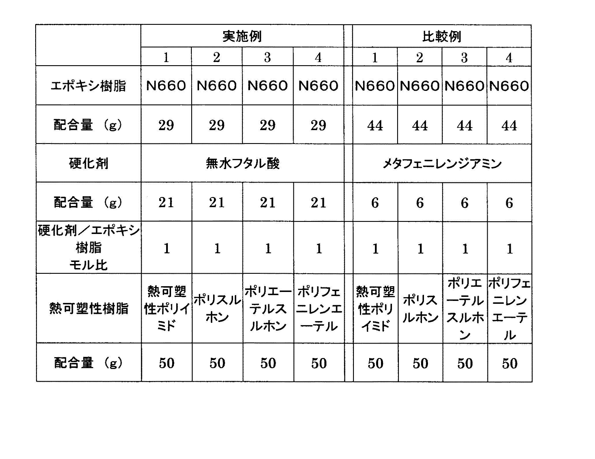
上記で得た熱可塑性ポリイミド樹脂、クレゾールノボラック型エポキシ樹脂(N660、エポキシ当量208g/eq、大日本インキ化学工業(株)社製)、無水フタル酸(酸無水物当量148g/eq)をジオキソランに加えて撹拌、溶解させ、樹脂組成物溶液を得た(固形分率(SC)=30%)。尚、配合量は表3に記載の通りとした。この溶液を、厚み125μmのPETフィルム(商品名セラピールHP、東洋メタライジング社製)の表面上にコンマコーターにて塗布後、熱風オーブンにて、60℃/1分、80℃/1分、100℃/3分、120℃/1分、150℃/3分の条件でステップ乾燥させて、シート厚みが40μmの半硬化状態のPETフィルム付き絶縁接着フィルムを得た。次に、PETフィルムを剥離し、絶縁接着フィルムをピン枠に固定し、180℃/60分加熱し、硬化フィルムを得た。次に、得られた硬化フィルムにデスミア処理を施した。このとき、デスミア前後での硬化フィルムの表面形状を観察した。その結果を表4に示す。
(Measurement condition)
Objective lens: 50x Mirau Image zoom: 2
FDA Res: Normal
Analysis conditions:
Remove: Cylinder
Filter: High Pass
Filter Low Wave: 0.002mm
[Measurement of adhesive strength]
IPC-TM-650-method. According to 2.4.9, measurement was performed at a pattern width of 3 mm, a peeling angle of 90 degrees, and a peeling speed of 50 mm / min. The pretreatment of the measurement sample was performed as follows.
Pretreatment: The measurement sample was left in a constant temperature room at 23 ° C. and 50% humidity for 24 hours.
(Example 1)
The thermoplastic polyimide resin obtained above, the cresol novolak type epoxy resin (N660, epoxy equivalent 208 g / eq, manufactured by Dainippon Ink & Chemicals, Inc.), phthalic anhydride (acid anhydride equivalent 148 g / eq) in dioxolane In addition, the mixture was stirred and dissolved to obtain a resin composition solution (solid content ratio (SC) = 30%). The blending amounts were as shown in Table 3. This solution was applied on the surface of a 125 μm thick PET film (trade name Therapy HP, manufactured by Toyo Metallizing Co., Ltd.) with a comma coater, and then heated in a hot air oven at 60 ° C./1 min, 80 ° C./1 min, 100 Step-drying was performed under the conditions of ° C / 3 minutes, 120 ° C / 1 minute, and 150 ° C / 3 minutes to obtain a semi-cured insulating adhesive film with a PET film having a sheet thickness of 40 μm. Next, the PET film was peeled off, the insulating adhesive film was fixed to the pin frame, and heated at 180 ° C./60 minutes to obtain a cured film. Next, the obtained cured film was subjected to desmear treatment. At this time, the surface shape of the cured film before and after desmear was observed. The results are shown in Table 4.
続いて、デスミア処理を施した硬化フィルムに無電解銅めっきおよび電解銅めっきを行い、厚さ約18μmの銅層を形成し、パターン幅3mmのパターニングを施した後、熱風オーブンで180℃、30分加熱した。このサンプルを用いてフィルムと無電解めっき銅との接着強度を測定した。その結果を表4に示す。 Subsequently, electroless copper plating and electrolytic copper plating were performed on the cured film subjected to desmear treatment to form a copper layer having a thickness of about 18 μm, patterning with a pattern width of 3 mm, and then performed at 180 ° C. in a hot air oven at 30 ° C. Heated for minutes. Using this sample, the adhesive strength between the film and electroless plated copper was measured. The results are shown in Table 4.
(実施例2〜4)
表3に示すように、熱可塑性樹脂を、ポリスルホン、ポリエーテルスルホン、ポリフェニレンエーテルとした以外は実施例1と同様にして、硬化フィルムを得た。
(Examples 2 to 4)
As shown in Table 3, a cured film was obtained in the same manner as in Example 1 except that the thermoplastic resin was polysulfone, polyethersulfone, or polyphenylene ether.
得られた硬化フィルムについて、表面粗度及び無電解めっき銅との接着強度を評価した。その結果を表4に示す。 About the obtained cured film, surface roughness and the adhesive strength with electroless-plated copper were evaluated. The results are shown in Table 4.
(実施例5)
銅箔18μmのガラスエポキシ銅張積層板から内層配線板を作製し、実施例1で得た半硬化状態のPETフィルム付き絶縁接着フィルムのPETフィルムを剥離し、絶縁接着フィルムと内層配線とを対向させ、真空プレスにより温度180℃、熱板圧力3MPa、プレス時間60分、真空条件1KPaの条件で内層配線板に積層し、積層体を得た。(尚、真空プレス時に絶縁接着フィルムと接する箇所の合紙には、Raが0.006μmであるフッ素樹脂フィルム(旭硝子(株)製アフレックス)を使用した。
上記積層体に、UV−YAGレーザーにより内層配線板の電極直上に該電極に至る内径30μmのビアホールを開け、続いて基板全面に無電解銅めっきを施した後180℃、30分の加熱処理を施した。その後、形成した銅めっき層上にレジストパターンを形成し、厚み10μmの電解銅めっきを施した後、レジストパターンを剥離し、さらに露出しためっき銅を塩酸/塩化第二鉄系エッチャントで除去して、L/S=10μm/10μmの配線を有するプリント配線板を作製した。表5に示すように、L/S=10μm/10μmの微細配線はほぼ設計値通りのライン/スペースを有し、配線形状は良好で、且つ配線剥がれは全くなかった。
(Example 5)
An inner layer wiring board was prepared from a glass epoxy copper clad laminate of 18 μm copper foil, the PET film of the semi-cured insulating film with PET film obtained in Example 1 was peeled off, and the insulating adhesive film and the inner layer wiring were opposed. The laminate was laminated by vacuum pressing on the inner wiring board under the conditions of a temperature of 180 ° C., a hot plate pressure of 3 MPa, a press time of 60 minutes, and a vacuum condition of 1 KPa. (In addition, a fluororesin film (Aflex manufactured by Asahi Glass Co., Ltd.) having an Ra of 0.006 μm was used as a slip sheet at a portion that contacts the insulating adhesive film during vacuum pressing.
In the laminate, a via hole having an inner diameter of 30 μm reaching the electrode is opened immediately above the electrode of the inner wiring board by a UV-YAG laser, followed by electroless copper plating on the entire surface of the substrate, followed by heat treatment at 180 ° C. for 30 minutes. gave. Thereafter, a resist pattern is formed on the formed copper plating layer, and after applying electrolytic copper plating with a thickness of 10 μm, the resist pattern is peeled off, and the exposed plated copper is removed with a hydrochloric acid / ferric chloride-based etchant. A printed wiring board having a wiring of L / S = 10 μm / 10 μm was produced. As shown in Table 5, the fine wiring with L / S = 10 μm / 10 μm had lines / spaces almost as designed, the wiring shape was good, and there was no wiring peeling.
(実施例6〜8)
実施例2〜4で作製した半硬化状態のPETフィルム付き絶縁接着フィルムを用いた以外は実施例5と同様にしてプリント配線板を作製した。表5に示すように、いずれのプリント配線板においてもL/S=10μm/10μmの微細配線はほぼ設計値通りのライン/スペースを有し、配線形状は良好で、且つ配線剥がれは全くなかった。
(Examples 6 to 8)
A printed wiring board was produced in the same manner as in Example 5 except that the semi-cured insulating adhesive film with a PET film produced in Examples 2 to 4 was used. As shown in Table 5, in any printed wiring board, fine wiring with L / S = 10 μm / 10 μm had lines / spaces almost as designed, the wiring shape was good, and there was no wiring peeling at all. .
(比較例1〜4)
無水フタル酸をメタフェニレンジアミン(アミン当量27g/eq)とし、表3に示す配合量にて配合した以外は実施例1と同様にして、硬化フィルムを得た。
得られた硬化フィルムについて、表面粗度及び無電解めっき銅との接着強度を評価した。その結果を表4に示す。
(Comparative Examples 1-4)
A cured film was obtained in the same manner as in Example 1, except that phthalic anhydride was metaphenylenediamine (amine equivalent 27 g / eq) and blended in the blending amounts shown in Table 3.
About the obtained cured film, surface roughness and the adhesive strength with electroless-plated copper were evaluated. The results are shown in Table 4.
(比較例5〜8)
比較例1〜4で得たPETフィルム付き絶縁接着フィルムを用いた以外は実施例5と同様にして、プリント配線板を作製した。表5に示すように、L/S=10μm/10μmの微細配線は、剥がれ落ちている箇所が存在した。
(Comparative Examples 5-8)
A printed wiring board was produced in the same manner as in Example 5 except that the insulating adhesive film with a PET film obtained in Comparative Examples 1 to 4 was used. As shown in Table 5, in the fine wiring with L / S = 10 μm / 10 μm, there was a part where it was peeled off.
Claims (7)
Priority Applications (1)
| Application Number | Priority Date | Filing Date | Title |
|---|---|---|---|
| JP2004116548A JP2005298670A (en) | 2004-04-12 | 2004-04-12 | Insulating adhesive film, printed wiring board |
Applications Claiming Priority (1)
| Application Number | Priority Date | Filing Date | Title |
|---|---|---|---|
| JP2004116548A JP2005298670A (en) | 2004-04-12 | 2004-04-12 | Insulating adhesive film, printed wiring board |
Publications (1)
| Publication Number | Publication Date |
|---|---|
| JP2005298670A true JP2005298670A (en) | 2005-10-27 |
Family
ID=35330606
Family Applications (1)
| Application Number | Title | Priority Date | Filing Date |
|---|---|---|---|
| JP2004116548A Pending JP2005298670A (en) | 2004-04-12 | 2004-04-12 | Insulating adhesive film, printed wiring board |
Country Status (1)
| Country | Link |
|---|---|
| JP (1) | JP2005298670A (en) |
Cited By (2)
| Publication number | Priority date | Publication date | Assignee | Title |
|---|---|---|---|---|
| JP2007294902A (en) * | 2006-03-28 | 2007-11-08 | Ngk Spark Plug Co Ltd | Wiring board manufacturing method |
| JP2018129548A (en) * | 2007-11-22 | 2018-08-16 | 味の素株式会社 | Method for manufacturing multilayer printed wiring board |
-
2004
- 2004-04-12 JP JP2004116548A patent/JP2005298670A/en active Pending
Cited By (2)
| Publication number | Priority date | Publication date | Assignee | Title |
|---|---|---|---|---|
| JP2007294902A (en) * | 2006-03-28 | 2007-11-08 | Ngk Spark Plug Co Ltd | Wiring board manufacturing method |
| JP2018129548A (en) * | 2007-11-22 | 2018-08-16 | 味の素株式会社 | Method for manufacturing multilayer printed wiring board |
Similar Documents
| Publication | Publication Date | Title |
|---|---|---|
| KR100767177B1 (en) | Adhesion Assisting Agent-Bearing Metal Foil, Printed Wiring Board, and Production Method of Printed Wiring Board | |
| KR100710119B1 (en) | Process for forming metal layer on resin layer, print distributing board and manufacturing method thereof | |
| CN100488766C (en) | Metal foil with resin attached thereto, metal-clad laminate, printed wiring board using the same, and method for manufacturing the same | |
| US20040231141A1 (en) | Laminate and its producing method | |
| TWI619761B (en) | Curable resin composition | |
| KR100910092B1 (en) | Metal foil provided with adhesion auxiliary material and printed wiring board using same | |
| KR20140121783A (en) | Curable resin composition | |
| JP2004025835A (en) | Resin coated metal foil, metal-clad laminate, printed wiring board using the same, and its manufacturing process | |
| JP5521099B1 (en) | Copper foil with carrier, printed wiring board, printed circuit board, copper-clad laminate, and printed wiring board manufacturing method | |
| JP5011641B2 (en) | Thermosetting resin composition, adhesive film using the same, and multilayer printed wiring board | |
| TWI627225B (en) | Hardenable epoxy composition, diaphragm, laminated diaphragm, prepreg, laminated body, cured body, and composite | |
| TWI894375B (en) | Resin composition, cured product, sheet laminate, resin sheet, printed wiring board, and semiconductor device | |
| JP2008258636A (en) | Internal layer conductor circuit treatment method | |
| JP4345554B2 (en) | Printed wiring board having an auxiliary adhesion layer between insulating layers and method for manufacturing the same | |
| KR20140102612A (en) | Curable resin composition | |
| JP2014159512A (en) | Curable resin composition | |
| JP2005167173A (en) | Method of forming insulating resin layer on metal, method of treating internal conductor circuit, method of manufacturing printed wiring board, and multilayered wiring board | |
| JP2005290327A (en) | Electrical insulation adhesive film and laminate containing the same, and printed wiring board | |
| JP2005298670A (en) | Insulating adhesive film, printed wiring board | |
| JP2001233945A (en) | Electroless-platable highly heat resistant epoxy resin composition, insulation material for buildup using it and buildup base plate | |
| JP2005135985A (en) | Manufacturing method for printed wiring board | |
| CN100546435C (en) | Forming method of resin layer of metal layer, printed wiring board and manufacturing method thereof | |
| JP2005223052A (en) | Manufacturing method for printed-wiring board | |
| JP2003133704A (en) | Adhesive sheet for circuit board and coverlay | |
| JP2018109195A (en) | Curable resin composition |