JP2005298601A - Epoxy resin molding material for semiconductor encapsulation and resin-encapsulated semiconductor device - Google Patents
Epoxy resin molding material for semiconductor encapsulation and resin-encapsulated semiconductor device Download PDFInfo
- Publication number
- JP2005298601A JP2005298601A JP2004114489A JP2004114489A JP2005298601A JP 2005298601 A JP2005298601 A JP 2005298601A JP 2004114489 A JP2004114489 A JP 2004114489A JP 2004114489 A JP2004114489 A JP 2004114489A JP 2005298601 A JP2005298601 A JP 2005298601A
- Authority
- JP
- Japan
- Prior art keywords
- epoxy resin
- group
- carbon black
- semiconductor device
- resin
- Prior art date
- Legal status (The legal status is an assumption and is not a legal conclusion. Google has not performed a legal analysis and makes no representation as to the accuracy of the status listed.)
- Pending
Links
- 0 CO[C@]1C=*CCC1 Chemical compound CO[C@]1C=*CCC1 0.000 description 3
- PFEOZAIUSHOKJA-VIFPVBQESA-N C([C@@H]1Oc2ccccc2)[N]11OC1 Chemical compound C([C@@H]1Oc2ccccc2)[N]11OC1 PFEOZAIUSHOKJA-VIFPVBQESA-N 0.000 description 1
Classifications
-
- H—ELECTRICITY
- H01—ELECTRIC ELEMENTS
- H01L—SEMICONDUCTOR DEVICES NOT COVERED BY CLASS H10
- H01L2924/00—Indexing scheme for arrangements or methods for connecting or disconnecting semiconductor or solid-state bodies as covered by H01L24/00
- H01L2924/0001—Technical content checked by a classifier
- H01L2924/0002—Not covered by any one of groups H01L24/00, H01L24/00 and H01L2224/00
Landscapes
- Compositions Of Macromolecular Compounds (AREA)
- Structures Or Materials For Encapsulating Or Coating Semiconductor Devices Or Solid State Devices (AREA)
Abstract
【課題】 成形性、信頼性、レーザーマーク性、電気特性に優れ、薄型、多ピン、ロングワイヤー、狭パッドピッチの半導体装置においても、導電性物質であるカーボンブラック起因の電気特性不良を発生させない封止材及びそれを用いた半導体装置を提供すること。
【解決手段】 (A)エポキシ樹脂、及び(B)45μmのふるい残分が8ppm以下のカーボンブラックを含む半導体封止用エポキシ樹脂組成物。
【選択図】 なしPROBLEM TO BE SOLVED: To provide excellent formability, reliability, laser mark property, and electrical characteristics, and does not cause defects in electrical characteristics due to carbon black, which is a conductive material, even in a thin, multi-pin, long wire, narrow pad pitch semiconductor device. A sealing material and a semiconductor device using the same are provided.
An epoxy resin composition for encapsulating a semiconductor comprising (A) an epoxy resin and (B) carbon black having a sieve residue of 45 μm of 8 ppm or less.
[Selection figure] None
Description
本発明は、半導体封止用エポキシ樹脂成形材料及びこれにより封止された樹脂封止型半導体装置に関する。 The present invention relates to an epoxy resin molding material for semiconductor encapsulation and a resin-encapsulated semiconductor device encapsulated thereby.
近年、電子部品のプリント配線板への高密度実装化が進んでいる。これに伴い、半導体装置は従来のピン挿入型のパッケージから、表面実装型のパッケージが主流になっている。表面実装型のIC、LSIなどは、実装密度を高くし実装高さを低くするために、薄型、小型のパッケージになっており、素子のパッケージに対する占有体積が大きくなり、パッケージの肉厚は非常に薄くなってきた。また素子の多機能化、大容量化によって、チップ面積の増大、多ピン化が進み、さらにはパッド(電極)数の増大によって、パッドピッチの縮小化とパッド寸法の縮小化、いわゆる狭パッドピッチ化も進んでおり、最近ではパッドピッチが60μm以下の半導体素子も現われてきている。
また、小型軽量化に対応すべく、パッケージの形態もQFP(Quad Flat Package)、SOP(Small Outline Package)といったものから、より多ピン化に対応しやすく、かつより高密度実装が可能なCSP(Chip Size Package)やBGA(Ball Grid Array)へ移行しつつある。これらのパッケージは近年、高速化、多機能化を実現するために、フェースダウン型、積層(スタックド)型、フリップチップ型、ウェハーレベル型等、新しい構造のものが開発されている。この中で、積層(スタックド)型はパッケージ内部に複数のチップを積み重ねてワイヤボンディングで接続する構造であり、機能の異なる複数のチップを一つのパッケージに搭載可能であるため、多機能化が可能となる。
これらの半導体装置内部では狭い領域に多数の金線が複雑に張り巡らされているため、封止材が一定以上の大きさの導電性粒子を含有していた場合高い確率で金線間に引っ掛かりショート不良が発生することになる。特に配線間隔の狭い有機基板、有機フィルム等の実装基板を使用した場合には、基板上の配線間を導電性物質が橋渡しすることによるリーク不良が発生し易い。この基板上の配線間の導電性物質による橋渡しは必ずしも一つの導電性粒子が引き起こすだけではなく、導電性の微粒子がチェーンのように繋がって配線間を橋渡しすることが知られている。このような微粒子の連鎖は低粘度の樹脂中に微粒子が分散し且つその微粒子が樹脂中を容易に移動し得る場合に特に発生し易い。
IC、LSI等の半導体チップは、チップの集積度の向上と共に、チップサイズの大型化、半導体装置の小型化、薄型化、多ピン化が進んでいる。さらに、電子機器の小型化、薄型化に対応し、実装方法も高密度実装を可能とする表面実装方式がピン挿入型方式に代わり、急速に普及している。その結果、半導体装置を基板へ取り付ける時に、半導体装置自体が短時間の内に200℃以上の半田浴といった高温に晒される。この時、封止材中に含まれる水分が気化し、ここで発生する蒸気圧が封止材と素子、リードフレーム等のインサートとの界面において剥離応力として働き、封止材とインサートとの間で剥離が発生し、特に薄型の半導体装置においては、半導体装置のフクレやクラックに至ってしまう。
このような剥離起因によるフクレ、クラックの防止策として、素子表面又はリードフレームのアイランド裏面にコート材を用い、封止材との密着性を向上されせる手法、リードフレームのアイランド裏面にディンプル加工やスリット加工等を行なう、あるいはLOC(Lead on Chip)構造にして封止材との密着性を向上させる手法が用いられているが、高コスト化、効果不十分等の問題がある。さらに、LOC構造の場合、パッケージ表面の色むらが生じ、外観を損ねている。
In recent years, high-density mounting of electronic components on printed wiring boards has been progressing. As a result, surface mount packages have become mainstream from conventional pin insertion packages. Surface-mount ICs, LSIs, etc. are thin and small packages in order to increase the mounting density and reduce the mounting height, and the volume occupied by the device package increases, resulting in a very thick package. It has become thinner. In addition, due to the increased functionality and capacity of the elements, the chip area is increased and the number of pins is increased, and further, the pad pitch is reduced and the pad size is reduced by increasing the number of pads (electrodes), so-called narrow pad pitch. In recent years, semiconductor elements having a pad pitch of 60 μm or less have also appeared.
In addition, in order to cope with the reduction in size and weight, CSP (Package Forms) such as QFP (Quad Flat Package), SOP (Small Outline Package), etc., which can easily cope with higher pin counts and can be mounted at higher density (CSP) It is shifting to Chip Size Package (BGA) and BGA (Ball Grid Array). In recent years, these packages have been developed with new structures such as a face-down type, a stacked (stacked) type, a flip chip type, and a wafer level type in order to realize high speed and multiple functions. Of these, the stacked type is a structure in which multiple chips are stacked inside the package and connected by wire bonding, and multiple chips with different functions can be mounted in a single package, enabling multiple functions. It becomes.
In these semiconductor devices, a large number of gold wires are intricately stretched in a narrow area, so if the encapsulant contains conductive particles of a certain size or larger, it is likely to be caught between the gold wires. Short circuit failure will occur. In particular, when a mounting substrate such as an organic substrate or an organic film having a narrow wiring interval is used, a leakage defect is likely to occur due to a conductive material bridging between the wirings on the substrate. It is known that the bridging of the conductive material between the wirings on the substrate is not necessarily caused by one conductive particle, but conductive fine particles are connected like a chain to bridge the wiring. Such a chain of fine particles is particularly likely to occur when the fine particles are dispersed in a low-viscosity resin and the fine particles can easily move in the resin.
Semiconductor chips such as ICs and LSIs are increasing in chip integration, increasing in chip size, downsizing, thinning, and increasing the number of pins of semiconductor devices. Furthermore, the surface mounting method that can cope with the downsizing and thinning of electronic devices and that can be mounted with high density is rapidly spreading instead of the pin insertion type. As a result, when the semiconductor device is attached to the substrate, the semiconductor device itself is exposed to a high temperature such as a solder bath of 200 ° C. or more within a short time. At this time, moisture contained in the sealing material is vaporized, and the vapor pressure generated here acts as a peeling stress at the interface between the sealing material and the insert of the element, lead frame, etc., and between the sealing material and the insert. Peeling occurs, and in particular in thin semiconductor devices, blisters and cracks of the semiconductor device are reached.
As a measure to prevent blisters and cracks due to such peeling, a coating material is used on the element surface or the back surface of the island of the lead frame to improve the adhesion with the sealing material, dimple processing on the back surface of the island of the lead frame, A technique of performing slit processing or the like or improving the adhesion to the sealing material by using a LOC (Lead on Chip) structure is used, but there are problems such as high cost and insufficient effect. Further, in the case of the LOC structure, the color of the package surface is uneven and the appearance is impaired.
一方、封止材には、半導体装置をプリント基板へ表面実装する際の懸案事項である耐リフロー性や、実装後の信頼性として要求される温度サイクル性等を高いレベルでクリアすることが求められ、樹脂粘度の低減とこれによる充填剤の高充填化によって封止材に低吸湿化と低膨張化を付与し対応を図ってきた。また半導体素子を光から保護し、レーザーマーク性を付与する等の目的で封止材中には着色剤として一般的にカーボンブラックが使用されている。カーボンブラックは導電性であるためカーボンブラックの粗粒子が存在すると先に述べたような電気特性不良の原因となる。時として樹脂の低粘度化は封止材製造時にカーボンブラックに掛る剪断応力を低減しカーボンブラックの凝集物の解砕を妨げてしまう。この結果、薄型、多ピン化された半導体装置用の高充填剤の封止材ほどカーボンブラック粗粒子が残り易く、パッケージの構造とあいまって電気特性不良発生の可能性が高くなる。これに対し例えば、予め無機充填材の内少なくとも50重量%以上とカーボンブラックを混合し、カーボンブラックの凝集物の最大粒径が100μm以下になるように分散させ、次いで他の配合物を混合した後溶融混練する半導体封止用エポキシ樹脂成形材料の製造方法(例えば、特許文献1参照。)、或いは平均粒子径10〜50nm、かつBrunauer−Emmett−Teller法による比表面積が80〜400m2/gであるカーボンブラックを必須成分とすることで凝集物を少なくすること(例えば、特許文献2参照)、カーボンブラックの比表面積、DPE吸油量、pH等を特定することで凝集物を少なくすること(例えば、特許文献3、4参照。)等が提案されている。
しかし、これらの方法では半導体封止用エポキシ樹脂成形材料の製造段階でカーボンブラックの凝集物を小さく、少なくすることは出来ても、半導体装置を製造するときのトランスファーモールド工程でのカーボンブラックの再凝集を防止することは困難であった。また達成できる凝集物の最大粒径も数十μm以下程度が限界であり、現在の狭パッドピッチ化の進展に対しては不充分なレベルであった。これに対応すべく、封止材にはさらなる凝集物の低減や製造条件の変更等による改良が試みられているが、未だ充分な結果を得てはいない。
また、着色剤としてカーボンブラックの代わりに有機染料、顔料等を用いた検討がなされている(例えば特許文献5、6参照。)が、YAGレーザーマーク性の低下、信頼性の低下、高コスト化等の問題があった。
On the other hand, the encapsulant is required to clear at a high level the reflow resistance, which is a matter of concern when the semiconductor device is surface-mounted on a printed circuit board, and the temperature cycle characteristics required for reliability after mounting. In order to cope with this problem, the resin has been reduced in moisture absorption and expansion due to the reduction in the resin viscosity and the increase in the filling of the filler. Carbon black is generally used as a colorant in the encapsulant for the purpose of protecting the semiconductor element from light and imparting laser mark properties. Since carbon black is electrically conductive, the presence of coarse particles of carbon black causes the above-described poor electrical characteristics. Occasionally, the lowering of the viscosity of the resin reduces the shear stress applied to the carbon black during the production of the sealing material, and prevents the carbon black aggregates from being crushed. As a result, the thinner the carbon black coarse particles are, the easier it is to seal the sealant with a high filler for a semiconductor device, and there is a high possibility of the occurrence of defective electrical characteristics in combination with the package structure. On the other hand, for example, at least 50% by weight or more of the inorganic filler and carbon black are mixed in advance and dispersed so that the maximum particle size of the aggregate of carbon black is 100 μm or less, and then another compound is mixed. A method for producing an epoxy resin molding material for semiconductor encapsulation that is post-melt kneaded (for example, see Patent Document 1), or an average particle diameter of 10 to 50 nm, and a specific surface area of 80 to 400 m 2 / g by Brunauer-Emmett-Teller method. The carbon black is an essential component to reduce aggregates (see, for example, Patent Document 2), and the specific surface area, DPE oil absorption, pH, etc. of the carbon black are specified to reduce aggregates ( For example, see Patent Documents 3 and 4).
However, in these methods, although carbon black aggregates can be reduced and reduced in the manufacturing stage of the epoxy resin molding material for semiconductor encapsulation, carbon black can be regenerated in the transfer molding process when manufacturing semiconductor devices. It was difficult to prevent aggregation. Further, the maximum particle size of the agglomerates that can be achieved is limited to about several tens of μm or less, which is insufficient for the current progress of narrow pad pitch. In order to cope with this, attempts have been made to improve the sealing material by further reducing aggregates or changing manufacturing conditions, but sufficient results have not yet been obtained.
In addition, studies have been made using organic dyes, pigments, etc., instead of carbon black as a colorant (see, for example, Patent Documents 5 and 6), but YAG laser mark property, reliability, and cost are increased. There was a problem such as.
本発明は、上記に鑑みてなされたものであって、成形性、信頼性、レーザーマーク性、電気特性に優れ、薄型、多ピン、ロングワイヤー、狭パッドピッチの半導体装置においても、導電性物質であるカーボンブラック起因の電気特性不良を発生させない封止材及びそれを用いた半導体装置を提供することを目的とする。 The present invention has been made in view of the above, and is excellent in moldability, reliability, laser mark property, and electrical characteristics, and is a conductive material even in a thin, multi-pin, long wire, narrow pad pitch semiconductor device. An object of the present invention is to provide a sealing material that does not cause a defective electrical characteristic due to carbon black and a semiconductor device using the same.
本発明は、エポキシ樹脂および45μmのふるい残分が8ppm以下のカーボンブラックを含有してなる半導体封止用エポキシ樹脂組成物及びこれにより封止された電気特性不良の発生が少ない半導体装置を提供しようとするものである。
1つの好適な態様において、本発明によれば、薄型、多ピン、ロングワイヤー、狭パッドピッチ、又は有機基板もしくは有機フィルム等の実装基板上に半導体チップが配置された半導体装置の封止に適した封止用エポキシ樹脂成形材料が提供される。
他の好適な態様において、本発明によれば、前記本発明に係る封止用エポキシ樹脂成形材料により封止された、薄型、多ピン、ロングワイヤー、狭パッドピッチ、又は有機基板もしくは有機フィルム等の実装基板上に半導体チップが配置された半導体装置が提供される。
An object of the present invention is to provide an epoxy resin composition for encapsulating a semiconductor comprising an epoxy resin and carbon black having a sieve residue of 45 μm of 8 ppm or less, and a semiconductor device encapsulated thereby, which is less likely to cause poor electrical characteristics. It is what.
In one preferred aspect, the present invention is suitable for sealing a semiconductor device in which a semiconductor chip is disposed on a thin substrate, a multi-pin, a long wire, a narrow pad pitch, or a mounting substrate such as an organic substrate or an organic film. An epoxy resin molding material for sealing is provided.
In another preferred embodiment, according to the present invention, a thin, multi-pin, long wire, narrow pad pitch, or organic substrate or organic film, etc., sealed with the sealing epoxy resin molding material according to the present invention. A semiconductor device in which a semiconductor chip is arranged on the mounting substrate is provided.
本発明は、
(1)(A)エポキシ樹脂及び(B)45μmのふるい残分が8ppm以下のカーボンブラックを含有する半導体封止用エポキシ樹脂組成物、
(2)(B)のカーボンブラック含有率が、0.1重量%〜10重量%であることを特徴とする(1)記載の半導体封止用エポキシ樹脂組成物、
(3)成形品表面を金属顕微鏡で評価した際のカーボンブラック粒径が50μm以下であることを特徴とする(1)又は(2)記載の半導体封止用エポキシ樹脂組成物、
(4)(1)〜(3)のいずれかに記載の半導体封止用エポキシ樹脂組成物を用いて半導体素子を封止してなる樹脂封止型半導体装置
に関する。
The present invention
(1) An epoxy resin composition for semiconductor encapsulation containing (A) an epoxy resin and (B) carbon black having a sieve residue of 45 μm of 8 ppm or less,
(2) The epoxy resin composition for semiconductor encapsulation according to (1), wherein the carbon black content of (B) is 0.1 wt% to 10 wt%,
(3) The epoxy resin composition for semiconductor encapsulation according to (1) or (2), wherein the carbon black particle size when the surface of the molded product is evaluated with a metal microscope is 50 μm or less,
(4) It is related with the resin-sealed semiconductor device formed by sealing a semiconductor element using the epoxy resin composition for semiconductor sealing in any one of (1)-(3).
本発明の半導体素子封止用エポキシ樹脂組成物はレーザーマーク性、電気特性、信頼性に優れた封止材及びそれを用いた半導体装置を得ることができる。 The epoxy resin composition for sealing a semiconductor element of the present invention can provide a sealing material excellent in laser mark properties, electrical characteristics, and reliability, and a semiconductor device using the same.
本発明において用いられるエポキシ樹脂は特に限定はないが、たとえば、電子部品封止用エポキシ樹脂成形材料で一般に使用されているもので、ビフェニル型エポキシ樹脂、ビフェニレン型エポキシ樹脂、フェノールノボラック型エポキシ樹脂、オルソクレゾールノボラック型エポキシ樹脂、ビスフェノ−ルAノボラック型エポキシ樹脂をはじめとするフェノール類及び/又はナフトール類とアルデヒド類から合成されるノボラック樹脂をエポキシ化したエポキシ樹脂、ビスフェノールA、ビスフェノールF、ビスフェノールS、アルキル置換ビフェノールなどのジグリシジルエーテル、スチルベン型エポキシ樹脂、ジアミノジフェニルメタン、イソシアヌル酸などのポリアミンとエピクロルヒドリンの反応により得られるグリシジルアミン型エポキシ樹脂、ジシクロペンタジエンとフェノ−ル類の共縮合樹脂のエポキシ化物であるジシクロペンタジエン型エポキシ樹脂、ナフタレン環を有するナフタレン型エポキシ樹脂、ナフトール・アラルキル樹脂のエポキシ化物、トリフェニルメタン型エポキシ樹脂トリメチロールプロパン型エポキシ樹脂、テルペン変性エポキシ樹脂、硫黄原子含有エポキシ樹脂、オレフィン結合を過酢酸などの過酸で酸化して得られる線状脂肪族エポキシ樹脂、及び脂環族エポキシ樹脂などが挙げられる。
なかでも、耐リフロー性の観点から、ビフェニル型エポキシ樹脂、ビスフェノールF型エポキシ樹脂、スチルベン型エポキシ樹脂及び硫黄原子含有エポキシ樹脂が好ましく、硬化性の観点からはノボラック型エポキシ樹脂が好ましく、低吸湿性の観点からはジシクロペンタジエン型エポキシ樹脂が好ましく、耐熱性及び低反り性の観点からはナフタレン型エポキシ樹脂及びトリフェニルメタン型エポキシ樹脂が好ましく、難燃性の観点からはビフェニレン型エポキシ樹脂が好ましく、これらのエポキシ樹脂の少なくとも1種を含有していることが好ましい。
The epoxy resin used in the present invention is not particularly limited. For example, it is generally used in an epoxy resin molding material for sealing electronic parts, and includes a biphenyl type epoxy resin, a biphenylene type epoxy resin, a phenol novolac type epoxy resin, Epoxy resins obtained by epoxidizing novolak resins synthesized from orthocresol novolac type epoxy resins, bisphenol A novolac type epoxy resins and / or phenols and / or naphthols and aldehydes, bisphenol A, bisphenol F, bisphenol S Glycidylamine obtained by the reaction of polychloroamines such as diglycidyl ethers such as alkyl-substituted biphenols, stilbene-type epoxy resins, diaminodiphenylmethane, and isocyanuric acid with epichlorohydrin Epoxy resin, dicyclopentadiene type epoxy resin which is an epoxidized product of co-condensation resin of dicyclopentadiene and phenols, naphthalene type epoxy resin having naphthalene ring, epoxidized product of naphthol / aralkyl resin, triphenylmethane type epoxy resin Examples include trimethylolpropane type epoxy resin, terpene modified epoxy resin, sulfur atom-containing epoxy resin, linear aliphatic epoxy resin obtained by oxidizing olefinic bonds with peracid such as peracetic acid, and alicyclic epoxy resin. .
Among them, biphenyl type epoxy resin, bisphenol F type epoxy resin, stilbene type epoxy resin and sulfur atom-containing epoxy resin are preferable from the viewpoint of reflow resistance, and novolak type epoxy resin is preferable from the viewpoint of curability, and low moisture absorption. From the viewpoint of the above, dicyclopentadiene type epoxy resin is preferable, from the viewpoint of heat resistance and low warpage, naphthalene type epoxy resin and triphenylmethane type epoxy resin are preferable, and from the viewpoint of flame retardancy, biphenylene type epoxy resin is preferable. It is preferable that at least one of these epoxy resins is contained.
ビフェニル型エポキシ樹脂としてはたとえば下記一般式(I)で示されるエポキシ樹脂等が挙げられ、ビスフェノールF型エポキシ樹脂としてはたとえば下記一般式(II)で示されるエポキシ樹脂等が挙げられ、スチルベン型エポキシ樹脂としてはたとえば下記一般式(III)で示されるエポキシ樹脂等が挙げられ、硫黄原子含有エポキシ樹脂としてはたとえば下記一般式(IV)で示されるエポキシ樹脂等が挙げられる。
Examples of the biphenyl type epoxy resin include an epoxy resin represented by the following general formula (I), and examples of the bisphenol F type epoxy resin include an epoxy resin represented by the following general formula (II), and a stilbene type epoxy resin. Examples of the resin include an epoxy resin represented by the following general formula (III), and examples of the sulfur atom-containing epoxy resin include an epoxy resin represented by the following general formula (IV).
上記一般式(I)で示されるビフェニル型エポキシ樹脂としては、たとえば、4,4’−ビス(2,3−エポキシプロポキシ)ビフェニル又は4,4’−ビス(2,3−エポキシプロポキシ)−3,3’,5,5’−テトラメチルビフェニルを主成分とするエポキシ樹脂、エピクロルヒドリンと4,4’−ビフェノール又は4,4’−(3,3’,5,5’−テトラメチル)ビフェノールとを反応させて得られるエポキシ樹脂等が挙げられる。なかでも4,4’−ビス(2,3−エポキシプロポキシ)−3,3’,5,5’−テトラメチルビフェニルを主成分とするエポキシ樹脂が好ましい。
上記一般式(II)で示されるビスフェノールF型エポキシ樹脂はとしては、例えば、R1、R3、R5及びR8がメチル基で、R2、R4、R5及びR7が水素原子であり、n=0を主成分とするYSLV−80XY(新日鉄化学株式会社製商品名)が市販品として入手可能である。
上記一般式(III)で示されるスチルベン型エポキシ樹脂は、原料であるスチルベン系フェノール類とエピクロルヒドリンとを塩基性物質存在下で反応させて得ることができる。この原料であるスチルベン系フェノール類としては、たとえば3−t−ブチル−4,4′−ジヒドロキシ−3′,5,5′−トリメチルスチルベン、3−t−ブチル−4,4′−ジヒドロキシ−3′,5′,6−トリメチルスチルベン、4,4’−ジヒドロキシ−3,3’,5,5’−テトラメチルスチルベン、4,4’−ジヒドロキシ−3,3’−ジ−t−ブチル−5,5’−ジメチルスチルベン、4,4’−ジヒドロキシ−3,3’−ジ−t−ブチル−6,6’−ジメチルスチルベン等が挙げられ、なかでも3−t−ブチル−4,4′−ジヒドロキシ−3′,5,5′−トリメチルスチルベン、及び4,4’−ジヒドロキシ−3,3’,5,5’−テトラメチルスチルベンが好ましい。これらのスチルベン型フェノール類は単独で用いても2種以上を組み合わせて用いてもよい。
上記一般式(IV)で示される硫黄原子含有エポキシ樹脂のなかでも、R2、R3、R5及びR7が水素原子で、R1、R4、R5及びR8がアルキル基であるエポキシ樹脂が好ましく、R2、R3、R5及びR7が水素原子で、R1及びR8がt−ブチル基で、R4及びR5がメチル基であるエポキシ樹脂がより好ましい。このような化合物としては、YSLV−120TE(新日鐵化学社製商品名)等が市販品として入手可能である。
Examples of the biphenyl type epoxy resin represented by the general formula (I) include 4,4′-bis (2,3-epoxypropoxy) biphenyl or 4,4′-bis (2,3-epoxypropoxy) -3. , 3 ′, 5,5′-tetramethylbiphenyl as the main component, epichlorohydrin and 4,4′-biphenol or 4,4 ′-(3,3 ′, 5,5′-tetramethyl) biphenol An epoxy resin obtained by reacting is used. Among these, an epoxy resin mainly composed of 4,4′-bis (2,3-epoxypropoxy) -3,3 ′, 5,5′-tetramethylbiphenyl is preferable.
Examples of the bisphenol F type epoxy resin represented by the general formula (II) include, for example, R 1 , R 3 , R 5 and R 8 are methyl groups, and R 2 , R 4 , R 5 and R 7 are hydrogen atoms. YSLV-80XY (trade name, manufactured by Nippon Steel Chemical Co., Ltd.) having n = 0 as a main component is commercially available.
The stilbene type epoxy resin represented by the above general formula (III) can be obtained by reacting a raw material stilbene phenol and epichlorohydrin in the presence of a basic substance. Examples of the raw material stilbene phenols include 3-t-butyl-4,4′-dihydroxy-3 ′, 5,5′-trimethylstilbene, 3-t-butyl-4,4′-dihydroxy-3. ', 5', 6-trimethylstilbene, 4,4'-dihydroxy-3,3 ', 5,5'-tetramethylstilbene, 4,4'-dihydroxy-3,3'-di-t-butyl-5 , 5'-dimethylstilbene, 4,4'-dihydroxy-3,3'-di-t-butyl-6,6'-dimethylstilbene and the like, among others, 3-t-butyl-4,4'- Dihydroxy-3 ', 5,5'-trimethylstilbene and 4,4'-dihydroxy-3,3', 5,5'-tetramethylstilbene are preferred. These stilbene type phenols may be used alone or in combination of two or more.
Among the sulfur atom-containing epoxy resins represented by the general formula (IV), R 2 , R 3 , R 5 and R 7 are hydrogen atoms, and R 1 , R 4 , R 5 and R 8 are alkyl groups. An epoxy resin is preferable, and an epoxy resin in which R 2 , R 3 , R 5, and R 7 are hydrogen atoms, R 1 and R 8 are t-butyl groups, and R 4 and R 5 are methyl groups is more preferable. As such a compound, YSLV-120TE (trade name, manufactured by Nippon Steel Chemical Co., Ltd.) and the like are commercially available.
ノボラック型エポキシ樹脂としては、たとえば下記一般式(V)で示されるエポキシ樹脂等が挙げられる。 Examples of the novolac type epoxy resin include an epoxy resin represented by the following general formula (V).
上記一般式(V)で示されるノボラック型エポキシ樹脂は、ノボラック型フェノール樹脂にエピクロルヒドリンを反応させることによって容易に得られる。なかでも、一般式(V)中のRとしては、メチル基、エチル基、プロピル基、ブチル基、イソプロピル基、イソブチル基等の炭素数1〜10のアルキル基、メトキシ基、エトキシ基、プロポキシ基、ブトキシ基等の炭素数1〜10のアルコキシル基が好ましく、水素原子又はメチル基がより好ましい。nは0〜3の整数が好ましい。上記一般式(V)で示されるノボラック型エポキシ樹脂のなかでも、オルトクレゾールノボラック型エポキシ樹脂が好ましい。
ノボラック型エポキシ樹脂を使用する場合、その配合量は、その性能を発揮するためにエポキシ樹脂全量に対して20重量%以上とすることが好ましく、30重量%以上がより好ましい。
The novolak type epoxy resin represented by the general formula (V) can be easily obtained by reacting a novolak type phenol resin with epichlorohydrin. Especially, as R in the general formula (V), an alkyl group having 1 to 10 carbon atoms such as a methyl group, an ethyl group, a propyl group, a butyl group, an isopropyl group, and an isobutyl group, a methoxy group, an ethoxy group, and a propoxy group C1-C10 alkoxyl groups, such as a butoxy group, are preferable, and a hydrogen atom or a methyl group is more preferable. n is preferably an integer of 0 to 3. Among the novolak epoxy resins represented by the general formula (V), orthocresol novolac epoxy resins are preferable.
In the case of using a novolac type epoxy resin, its blending amount is preferably 20% by weight or more, more preferably 30% by weight or more, based on the total amount of the epoxy resin in order to exhibit its performance.
ジシクロペンタジエン型エポキシ樹脂としては、たとえば下記一般式(VI)で示されるエポキシ樹脂等が挙げられる。 Examples of the dicyclopentadiene type epoxy resin include an epoxy resin represented by the following general formula (VI).
上記式(VI)中のR1としては、たとえば、水素原子、メチル基、エチル基、プロピル基、ブチル基、イソプロピル基、t−ブチル基等のアルキル基、ビニル基、アリル基、ブテニル基等のアルケニル基、ハロゲン化アルキル基、アミノ基置換アルキル基、メルカプト基置換アルキル基などの炭素数1〜5の置換又は非置換の一価の炭化水素基が挙げられ、なかでもメチル基、エチル基等のアルキル基及び水素原子が好ましく、メチル基及び水素原子がより好ましい。R2としては、たとえば、水素原子、メチル基、エチル基、プロピル基、ブチル基、イソプロピル基、t−ブチル基等のアルキル基、ビニル基、アリル基、ブテニル基等のアルケニル基、ハロゲン化アルキル基、アミノ基置換アルキル基、メルカプト基置換アルキル基などの炭素数1〜5の置換又は非置換の一価の炭化水素基が挙げられ、なかでも水素原子が好ましい。
ジシクロペンタジエン型エポキシ樹脂を使用する場合、その配合量は、その性能を発揮するためにエポキシ樹脂全量に対して20重量%以上とすることが好ましく、30重量%以上がより好ましい。
Examples of R 1 in the above formula (VI) include a hydrogen atom, an alkyl group such as a methyl group, an ethyl group, a propyl group, a butyl group, an isopropyl group, and a t-butyl group, a vinyl group, an allyl group, and a butenyl group. C1-C5 substituted or unsubstituted monovalent hydrocarbon groups such as alkenyl groups, halogenated alkyl groups, amino group-substituted alkyl groups, mercapto group-substituted alkyl groups, and the like. Among them, methyl groups, ethyl groups Alkyl groups and hydrogen atoms such as methyl groups and hydrogen atoms are more preferable. Examples of R 2 include a hydrogen atom, an alkyl group such as a methyl group, an ethyl group, a propyl group, a butyl group, an isopropyl group, and a t-butyl group, an alkenyl group such as a vinyl group, an allyl group, and a butenyl group, and an alkyl halide. Examples thereof include substituted or unsubstituted monovalent hydrocarbon groups having 1 to 5 carbon atoms such as a group, an amino group-substituted alkyl group, and a mercapto group-substituted alkyl group, and among them, a hydrogen atom is preferable.
When a dicyclopentadiene type epoxy resin is used, its blending amount is preferably 20% by weight or more, more preferably 30% by weight or more based on the total amount of the epoxy resin in order to exhibit its performance.
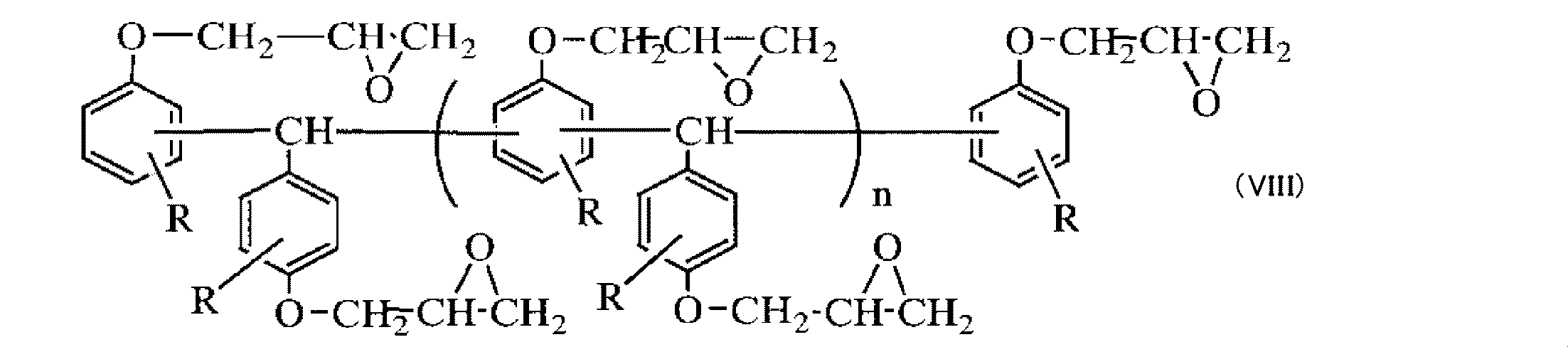
ナフタレン型エポキシ樹脂としてはたとえば下記一般式(VII)で示されるエポキシ樹脂等が挙げられ、トリフェニルメタン型エポキシ樹脂としてはたとえば下記一般式(VIII)で示されるエポキシ樹脂等が挙げられる。 Examples of the naphthalene type epoxy resin include an epoxy resin represented by the following general formula (VII), and examples of the triphenylmethane type epoxy resin include an epoxy resin represented by the following general formula (VIII).
上記一般式(VII)で示されるナフタレン型エポキシ樹脂としては、l個の構成単位及びm個の構成単位をランダムに含むランダム共重合体、交互に含む交互共重合体、規則的に含む共重合体、ブロック状に含むブロック共重合体が挙げられ、これらのいずれか1種を単独で用いても、2種以上を組み合わせて用いてもよい。
The naphthalene type epoxy resin represented by the general formula (VII) includes a random copolymer containing 1 constituent unit and m constituent units at random, an alternating copolymer containing alternating units, and a copolymer containing regularly. Examples thereof include block copolymers which are included in a combined or block form, and any one of these may be used alone, or two or more may be used in combination.
ビフェニレン型エポキシ樹脂としては例えば下記一般式(IX)で示されるエポキシ樹脂が挙げられる。 Examples of the biphenylene type epoxy resin include an epoxy resin represented by the following general formula (IX).
上記のビフェニル型エポキシ樹脂、ビフェニレン型エポキシ樹脂、スチルベン型エポキシ樹脂、硫黄原子含有エポキシ樹脂、ノボラック型エポキシ樹脂、ジシクロペンタジエン型エポキシ樹脂、ナフタレン型エポキシ樹脂及びトリフェニルメタン型エポキシ樹脂は、いずれか1種を単独で用いても2種以上を組合わせて用いてもよいが、その配合量はエポキシ樹脂全量に対して合わせて50重量%以上とすることが好ましく、60重量%以上がより好ましく、80重量%以上がさらに好ましい。
本発明において用いられる(A)エポキシ樹脂の150℃における溶融粘度は、流動性の観点から2ポイズ以下が好ましく、1.0ポイズ以下がより好ましく、0.5ポイズ以下がさらに好ましい。ここで、溶融粘度とはICIコーンプレート粘度計で測定した粘度を示す。
Any of the above biphenyl type epoxy resin, biphenylene type epoxy resin, stilbene type epoxy resin, sulfur atom-containing epoxy resin, novolac type epoxy resin, dicyclopentadiene type epoxy resin, naphthalene type epoxy resin and triphenylmethane type epoxy resin One type may be used alone or two or more types may be used in combination, but the blending amount is preferably 50% by weight or more, more preferably 60% by weight or more, based on the total amount of the epoxy resin. 80% by weight or more is more preferable.
The melt viscosity at 150 ° C. of the (A) epoxy resin used in the present invention is preferably 2 poises or less, more preferably 1.0 poises or less, and even more preferably 0.5 poises or less from the viewpoint of fluidity. Here, the melt viscosity is a viscosity measured with an ICI cone plate viscometer.
本発明において用いることのできる硬化剤は、封止用エポキシ樹脂成形材料に一般に使用されているもので特に制限はないが、たとえば、フェノール、クレゾール、レゾルシン、カテコール、ビスフェノールA、ビスフェノールF、フェニルフェノール、アミノフェノール等のフェノール類及び/又はα−ナフトール、β−ナフトール、ジヒドロキシナフタレン等のナフトール類とホルムアルデヒド、ベンズアルデヒド、サリチルアルデヒド等のアルデヒド基を有する化合物とを酸性触媒下で縮合又は共縮合させて得られるノボラック型フェノール樹脂、フェノール類及び/又はナフトール類とジメトキシパラキシレン又はビス(メトキシメチル)ビフェニルから合成されるフェノール・アラルキル樹脂、ナフトール・アラルキル樹脂等のアラルキル型フェノール樹脂、フェノール類及び/又はナフトール類とシクロペンタジエンから共重合により合成されるジシクロペンタジエン型フェノールノボラック樹脂、ナフトールノボラック樹脂等のジシクロペンタジエン型フェノール樹脂、テルペン変性フェノール樹脂などが挙げられ、これらを単独で用いても2種以上を組み合わせて用いてもよい。
なかでも、難燃性の観点からはビフェニル型フェノール樹脂が好ましく、耐リフロー性及び硬化性の観点からはアラルキル型フェノール樹脂が好ましく、低吸湿性の観点からはジシクロペンタジエン型フェノール樹脂が好ましく、耐熱性、低膨張率及び低そり性の観点からはトリフェニルメタン型フェノール樹脂が好ましく、硬化性の観点からはノボラック型フェノール樹脂が好ましく、これらのフェノール樹脂の少なくとも1種を含有していることが好ましい。
Curing agents that can be used in the present invention are generally used for sealing epoxy resin molding materials and are not particularly limited. For example, phenol, cresol, resorcin, catechol, bisphenol A, bisphenol F, and phenylphenol. Phenols such as aminophenol and / or naphthols such as α-naphthol, β-naphthol, dihydroxynaphthalene and the like and compounds having an aldehyde group such as formaldehyde, benzaldehyde, salicylaldehyde, etc., are condensed or co-condensed in the presence of an acidic catalyst. The resulting novolak-type phenolic resin, phenols and / or naphthols and dimethoxyparaxylene or bis (methoxymethyl) biphenyl synthesized aralkyl resins such as phenol aralkyl resins and naphthol aralkyl resins Examples include ruyl type phenol resins, dicyclopentadiene type phenol novolak resins synthesized by copolymerization from phenols and / or naphthols and cyclopentadiene, dicyclopentadiene type phenol resins such as naphthol novolak resins, and terpene-modified phenol resins. These may be used alone or in combination of two or more.
Among them, biphenyl type phenol resin is preferable from the viewpoint of flame retardancy, aralkyl type phenol resin is preferable from the viewpoint of reflow resistance and curability, and dicyclopentadiene type phenol resin is preferable from the viewpoint of low hygroscopicity, From the viewpoints of heat resistance, low expansion rate and low warpage, a triphenylmethane type phenol resin is preferable, and from the viewpoint of curability, a novolac type phenol resin is preferable, and contains at least one of these phenol resins. Is preferred.
ビフェニル型フェノール樹脂としては、たとえば下記一般式(X)で示されるフェノール樹脂等が挙げられる。
Examples of the biphenyl type phenol resin include a phenol resin represented by the following general formula (X).
上記一般式(X)で示されるビフェニル型フェノール樹脂としては、たとえばR1〜R9が全て水素原子である化合物等が挙げられ、なかでも溶融粘度の観点から、nが1以上の縮合体を50重量%以上含む縮合体の混合物が好ましい。このような化合物としては、MEH−7851(明和化成株式会社製商品名)が市販品として入手可能である。
ビフェニル型フェノール樹脂を使用する場合、その配合量は、その性能を発揮するために硬化剤全量に対して30重量%以上とすることが好ましく、50重量%以上がより好ましく、60重量%以上がさらに好ましい。
Examples of the biphenyl type phenol resin represented by the general formula (X) include compounds in which R 1 to R 9 are all hydrogen atoms, and in particular, from the viewpoint of melt viscosity, a condensate having n of 1 or more is used. A mixture of condensates containing 50% by weight or more is preferred. As such a compound, MEH-7851 (trade name, manufactured by Meiwa Kasei Co., Ltd.) is commercially available.
When a biphenyl type phenol resin is used, its blending amount is preferably 30% by weight or more, more preferably 50% by weight or more, more preferably 60% by weight or more based on the total amount of the curing agent in order to exhibit its performance. Further preferred.
アラルキル型フェノール樹脂としては、たとえばフェノール・アラルキル樹脂、ナフトール・アラルキル樹脂等が挙げられ、下記一般式(XI)で示されるフェノール・アラルキル樹脂が好ましく、一般式(XI)中のRが水素原子で、nの平均値が0〜8であるフェノール・アラルキル樹脂がより好ましい。具体例としては、p−キシリレン型フェノール・アラルキル樹脂、m−キシリレン型フェノール・アラルキル樹脂等が挙げられる。これらのアラルキル型フェノール樹脂を用いる場合、その配合量は、その性能を発揮するために硬化剤全量に対して30重量%以上とすることが好ましく、50重量%以上がより好ましい。 Examples of the aralkyl type phenol resin include a phenol aralkyl resin, a naphthol aralkyl resin, etc., and a phenol aralkyl resin represented by the following general formula (XI) is preferable, and R in the general formula (XI) is a hydrogen atom. , A phenol / aralkyl resin having an average value of n of 0 to 8 is more preferable. Specific examples include p-xylylene type phenol / aralkyl resins, m-xylylene type phenol / aralkyl resins, and the like. When using these aralkyl type phenol resins, the blending amount is preferably 30% by weight or more, more preferably 50% by weight or more, based on the total amount of the curing agent in order to exhibit the performance.
ジシクロペンタジエン型フェノール樹脂としては、たとえば下記一般式(XII)で示されるフェノール樹脂等が挙げられる。 Examples of the dicyclopentadiene type phenol resin include a phenol resin represented by the following general formula (XII).
ジシクロペンタジエン型フェノール樹脂を用いる場合、その配合量は、その性能を発揮するために硬化剤全量に対して30重量%以上とすることが好ましく、50重量%以上がより好ましい。
When a dicyclopentadiene type phenol resin is used, the blending amount is preferably 30% by weight or more, more preferably 50% by weight or more, based on the total amount of the curing agent in order to exhibit its performance.
トリフェニルメタン型フェノール樹脂としては、たとえば下記一般式(XIII)で示されるフェノール樹脂等が挙げられる。 Examples of the triphenylmethane type phenol resin include a phenol resin represented by the following general formula (XIII).
トリフェニルメタン型フェノール樹脂を用いる場合、その配合量は、その性能を発揮するために硬化剤全量に対して30重量%以上とすることが好ましく、50重量%以上がより好ましい。
これらの硬化剤は単独又は2種類以上併用して用いることができる。
When using a triphenylmethane type phenol resin, the blending amount is preferably 30% by weight or more, more preferably 50% by weight or more, based on the total amount of the curing agent in order to exhibit its performance.
These curing agents can be used alone or in combination of two or more.
また、(A)成分のエポキシ樹脂と硬化剤の当量比、すなわち、エポキシ樹脂中のエポキシ基数/硬化剤中の水酸基数の比は、特に限定はされないが、それぞれの未反応分を少なく抑えるために0.7〜1.3の範囲に設定することが好ましく、特に成形性、耐リフロー性に優れる成形材料を得るためには0.8〜1.2の範囲に設定することが好ましい。0.5当量未満ではエポキシ樹脂の硬化が不十分となり、硬化物の耐熱性、耐湿性並びに電気特性が劣る。また、1.5当量を超えると硬化剤成分が過剰になり硬化樹脂中に多量のフェノール性水酸基が残るため、電気特性並びに耐湿性が悪くなる。 In addition, the equivalent ratio of the epoxy resin and the curing agent of component (A), that is, the ratio of the number of epoxy groups in the epoxy resin / the number of hydroxyl groups in the curing agent is not particularly limited. In order to obtain a molding material excellent in moldability and reflow resistance, it is preferably set in the range of 0.8 to 1.2. If it is less than 0.5 equivalent, curing of the epoxy resin becomes insufficient, and the heat resistance, moisture resistance and electrical properties of the cured product are inferior. On the other hand, if it exceeds 1.5 equivalents, the curing agent component becomes excessive and a large amount of phenolic hydroxyl group remains in the cured resin, resulting in poor electrical characteristics and moisture resistance.
本発明において用いることのできる硬化促進剤は、封止用エポキシ樹脂成形材料に一般に使用されているもので特に制限はない。例えば、1,8−ジアザ−ビシクロ(5,4,0)ウンデセン−7、1,5−ジアザ−ビシクロ(4,3,0)ノネン、5、6−ヂブチルアミノ−1,8−ジアザ−ビシクロ(5,4,0)ウンデセン−7、ベンジルジメチルアミン、トリエタノールアミン、ジメチルアミノエタノール、トリス(ジメチルアミノメチル)フェノール等の3級アミン類及びこれらの誘導体、2−メチルイミダゾール、2−フェニルイミダゾール、2−フェニル−4−メチルイミダゾール等のイミダゾール類及びこれらの誘導体、トリブチルホスフィン、メチルジフェニルホスフィン、トリフェニルホスフィン、ジフェニルホスフィン、フェニルホスフィン等の有機ホスフィン類及びこれらのホスフィン類に無水マレイン酸、ベンゾキノン、ジアゾフェニルメタン等のπ結合をもつ化合物を付加してなる分子内分極を有するリン化合物、テトラフェニルホスホニウムテトラフェニルボレート、トリフェニルホスフィンテトラフェニルボレート、2−エチル−4−メチルイミダゾールテトラフェニルボレート、N−メチルモリホリンテトラフェニルボレート等のテトラフェニルボロン塩及びこれらの誘導体等があげられる。これらは、単独でも2種以上併用して用いても良い。 The curing accelerator that can be used in the present invention is not particularly limited, and is generally used for an epoxy resin molding material for sealing. For example, 1,8-diaza-bicyclo (5,4,0) undecene-7,1,5-diaza-bicyclo (4,3,0) nonene, 5,6-dibutylamino-1,8-diaza-bicyclo ( 5,4,0) undecene-7, benzyldimethylamine, triethanolamine, dimethylaminoethanol, tertiary amines such as tris (dimethylaminomethyl) phenol and their derivatives, 2-methylimidazole, 2-phenylimidazole, Imidazoles such as 2-phenyl-4-methylimidazole and derivatives thereof, organic phosphines such as tributylphosphine, methyldiphenylphosphine, triphenylphosphine, diphenylphosphine, and phenylphosphine, and maleic anhydride, benzoquinone, Diazophenyl meta Phosphorus compounds having intramolecular polarization formed by adding a compound having a π bond such as tetraphenylphosphonium tetraphenyl borate, triphenylphosphine tetraphenyl borate, 2-ethyl-4-methylimidazole tetraphenyl borate, N-methyl molybdate Examples thereof include tetraphenylboron salts such as holin tetraphenylborate and derivatives thereof. These may be used alone or in combination of two or more.
カップリング剤については、特に制限はなく、シランカップリング剤以外に従来公知のカップリング剤を併用してもよい。たとえば、ビニルトリクロロシラン、ビニルトリエトキシシラン、ビニルトリス(β−メトキシエトキシ)シラン、γ−メタクリロキシプロピルトリメトキシシラン、β−(3,4−エポキシシクロヘキシル)エチルトリメトキシシラン、γ−グリシドキシプロピルトリメトキシシラン、ビニルトリアセトキシシラン、γ−メルカプトプロピルトリメトキシシラン、γ−アミノプロピルトリエトキシシラン、γ−[ビス(β−ヒドロキシエチル)]アミノプロピルトリエトキシシラン、N−β−(アミノエチル)−γ−アミノプロピルトリメトキシシラン、γ−(β−アミノエチル)アミノプロピルジメトキシメチルシラン、N−(トリメトキシシリルプロピル)エチレンジアミン、N−(ジメトキシメチルシリルイソプロピル)エチレンジアミン、メチルトリメトキシシラン、メチルトリエトキシシラン、N−β−(N−ビニルベンジルアミノエチル)−γ−アミノプロピルトリメトキシシラン、γ−クロロプロピルトリメトキシシラン、ヘキサメチルジシラン、γ−アニリノプロピルトリメトキシシラン、ビニルトリメトキシシラン、γ−メルカプトプロピルメチルジメトキシシラン等のシラン系カップリング剤、あるいはイソプロピルトリイソステアロイルチタネート、イソプロピルトリス(ジオクチルパイロホスフェート)チタネート、イソプロピルトリ(N−アミノエチル−アミノエチル)チタネート、テトラオクチルビス(ジトリデシルホスファイト)チタネート、テトラ(2,2−ジアリルオキシメチル−1−ブチル)ビス(ジトリデシル)ホスファイトチタネート、ビス(ジオクチルパイロホスフェート)オキシアセテートチタネート、ビス(ジオクチルパイロホスフェート)エチレンチタネート、イソプロピルトリオクタノイルチタネート、イソプロピルジメタクリルイソステアロイルチタネート、イソプロピルトリドデシルベンゼンスルホニルチタネート、イソプロピルイソステアロイルジアクリルチタネート、イソプロピルトリ(ジオクチルホスフェート)チタネート、イソプロピルトリクミルフェニルチタネート、テトライソプロピルビス(ジオクチルホスファイト)チタネート等のチタネート系カップリング剤を1種以上併用することができる。 There is no restriction | limiting in particular about a coupling agent, You may use a conventionally well-known coupling agent together with a silane coupling agent. For example, vinyltrichlorosilane, vinyltriethoxysilane, vinyltris (β-methoxyethoxy) silane, γ-methacryloxypropyltrimethoxysilane, β- (3,4-epoxycyclohexyl) ethyltrimethoxysilane, γ-glycidoxypropyl Trimethoxysilane, vinyltriacetoxysilane, γ-mercaptopropyltrimethoxysilane, γ-aminopropyltriethoxysilane, γ- [bis (β-hydroxyethyl)] aminopropyltriethoxysilane, N-β- (aminoethyl) -Γ-aminopropyltrimethoxysilane, γ- (β-aminoethyl) aminopropyldimethoxymethylsilane, N- (trimethoxysilylpropyl) ethylenediamine, N- (dimethoxymethylsilylisopropyl) ethylenediamine, Tiltrimethoxysilane, methyltriethoxysilane, N-β- (N-vinylbenzylaminoethyl) -γ-aminopropyltrimethoxysilane, γ-chloropropyltrimethoxysilane, hexamethyldisilane, γ-anilinopropyltrimethoxy Silane coupling agents such as silane, vinyltrimethoxysilane, γ-mercaptopropylmethyldimethoxysilane, or isopropyltriisostearoyl titanate, isopropyltris (dioctylpyrophosphate) titanate, isopropyltri (N-aminoethyl-aminoethyl) titanate Tetraoctyl bis (ditridecyl phosphite) titanate, tetra (2,2-diallyloxymethyl-1-butyl) bis (ditridecyl) phosphite titanate, bis (dio Tylpyrophosphate) oxyacetate titanate, bis (dioctylpyrophosphate) ethylene titanate, isopropyltrioctanoyl titanate, isopropyldimethacrylisostearoyl titanate, isopropyltridodecylbenzenesulfonyl titanate, isopropylisostearoyl diacryl titanate, isopropyltri (dioctylphosphate) One or more titanate coupling agents such as titanate, isopropyl tricumylphenyl titanate, and tetraisopropyl bis (dioctyl phosphite) titanate can be used in combination.
離型剤についても、特に制限はないが、天然ワックス、合成ワックス、酸化または非酸化のポリオレフィン等の離型剤、例えばカルナバワックス等とポリエチレン系ワックスを単独又は併用して用いることができる。 The release agent is not particularly limited, but a release agent such as natural wax, synthetic wax, oxidized or non-oxidized polyolefin, such as carnauba wax and polyethylene wax can be used alone or in combination.
本発明において用いることのできる無機充填剤としては、特に限定はないが、溶融シリカ、結晶シリカ、アルミナ、ジルコン、珪酸カルシウム、炭酸カルシウム、炭化珪素、窒化アルミ、窒化ホウ素、ベリリア、ジルコニア等の粉体、又はこれらを球形化したビーズ、チタン酸カリウム、炭化珪素、窒化珪素、アルミナ等の単結晶繊維、ガラス繊維等を1種類以上配合して用いることができる。さらに、難燃効果のある無機充填剤としては水酸化アルミニウム、水酸化マグネシウム、硼酸亜鉛などが挙げられ、これらを単独または併用して用いることもできる。上記の無機充填剤の中で、線膨張係数低減の観点からは溶融シリカが、高熱伝導性の観点からはアルミナが好ましい。充填剤形状は、成形時の流動性及び金型摩耗性の点から球形もしくは球状に近い形が好ましく、50重量%以上が球形であることが特に好ましい。水分遮蔽性、金型磨耗等の観点から充填剤の平均粒径は15μm以下(充填剤の50重量%以上が15μm以下の粒径であること)が好ましく、10μm以下であることが特に好ましい。
無機充填剤の配合量は、吸湿性、線膨張係数の低減及び強度向上の観点から、成形材料全体に対して70重量%以上が好ましく、80〜95重量%であることが特に好ましい。70重量%未満では強度が低下しやすく、95重量%を超える場合には流動性が不足しがちである。中でも80〜90重量%の範囲がさらに好適である。
The inorganic filler that can be used in the present invention is not particularly limited, but powders such as fused silica, crystalline silica, alumina, zircon, calcium silicate, calcium carbonate, silicon carbide, aluminum nitride, boron nitride, beryllia, zirconia, etc. One or more kinds of spheres, beads obtained by spheroidizing them, single crystal fibers such as potassium titanate, silicon carbide, silicon nitride, and alumina, glass fibers, and the like can be used. Furthermore, examples of the inorganic filler having a flame retardant effect include aluminum hydroxide, magnesium hydroxide, zinc borate and the like, and these can be used alone or in combination. Among the inorganic fillers, fused silica is preferable from the viewpoint of reducing the linear expansion coefficient, and alumina is preferable from the viewpoint of high thermal conductivity. The shape of the filler is preferably spherical or nearly spherical from the viewpoint of fluidity during molding and mold wear, and particularly preferably 50% by weight or more is spherical. From the viewpoint of moisture shielding properties, mold wear, and the like, the average particle size of the filler is preferably 15 μm or less (50% by weight or more of the filler has a particle size of 15 μm or less), and particularly preferably 10 μm or less.
The blending amount of the inorganic filler is preferably 70% by weight or more, particularly preferably 80 to 95% by weight, based on the whole molding material, from the viewpoint of hygroscopicity, reduction of linear expansion coefficient and improvement of strength. If it is less than 70% by weight, the strength tends to decrease, and if it exceeds 95% by weight, the fluidity tends to be insufficient. Among these, the range of 80 to 90% by weight is more preferable.
カーボンブラックとして45μmふるい残分が8ppm以下のカーボンブラックを用いることにより良好な電気特性が得られ、5ppm以下のカーボンブラックを用いることにより更に良好な電気特性を得ることができる。ふるい残分の試験原理は、一定の条件下の水流でふるいを通して、既知量のカーボンブラックを洗浄し、ふるい残分を乾燥し、秤量する。ふるい残分の試験方法は、次の通りである。(JIS K 6218)
1)試験前に配水管のフィルターを洗浄する。
2)水圧を0.2±0.04Mpaに調整する。指定されたふるい(JIS Z 880 1に規定する標準網ふるいの目開き500μm、500μm、180μm、150μ m、125μm、75μm、45μm)を漏斗又は容器に取り付け、水を流し、3分 間洗浄する。ふるいの上に異物がないことを確認する。
3)試料約100gを0.1gまで正しく量りとる。
4)水を流し始める。試料を漏斗又は容器に入れる。試料の供給はふるいが目詰まりしな いように注意する。
5)試料を漏斗又は容器からカーボンブラックを洗い流す。ふるいを通過した洗浄水が透 明になるまで洗浄を続ける。
6)ふるいを取り外しふるい上の残分を指で軽くすりつぶす。このときふるいの目がゆが められるほどの圧力を加えてはならない。
7)ふるいを元に戻し水洗をさらに2分間行う。
8)ふるいを取り外し、乾燥機で105±2℃又は125±2℃で1時間乾燥する。
9)秤量した秤量皿にふるい残分を移し、0.1mgまで正しく量り採る。
10)次の式によって、ふるい残分を算出する。
R=(m1/m0)×100
(Rはふるい残分(%)、m1は加熱乾燥後のふるい残分の質量(g)、m0は試 料の質量(g)。)
カーボンブラックは、各種の炭化水素を不完全燃焼して得られる微細な球状粒子の集合体であり、アセチレン法によるアセチレンブラック、ファーネス法によるファーネスブラック、シェル法のガス化炉による特殊カーボンブラック等が挙げられ、これらを適宜何種類でも併用することができる。
また、カーボンブラックの粒子径、窒素吸着比表面積、DBP吸収量は、それぞれ黒色度及びカーボンブラックの分散性、凝集性の観点から10〜100nm、10〜500m2/g、30〜200cm3/100gが好ましく、より好ましくは、13〜80nm、30〜400m2/g、50〜150cm3/100gの範囲である。さらに、カーボンブラックの含有量は、組成物全体に対し、0.1〜10重量%が好ましい。その理由としては、組成全体の0.1重量%未満では、パッケージ表面の外観が損なわれる傾向が有り、さらには、遮光性、レーザーマーク性が不十分となる傾向があるためである。また、10重量%を超えるとでは成形性が不十分となり易いためである。さらに好ましい含有量は、0.1〜4重量%の範囲である。
Good electrical characteristics can be obtained by using carbon black with a carbon black having a 45 μm sieve residue of 8 ppm or less as carbon black, and even better electrical characteristics can be obtained by using 5 ppm or less of carbon black. The testing principle of the sieve residue is that a known amount of carbon black is washed through a sieve with a stream of water under certain conditions, the sieve residue is dried and weighed. The test method for the sieve residue is as follows. (JIS K 6218)
1) Wash the water pipe filter before the test.
2) Adjust the water pressure to 0.2 ± 0.04 Mpa. Attach the designated sieve (standard mesh sieve openings specified in JIS Z 880 1 to 500 μm, 500 μm, 180 μm, 150 μm, 125 μm, 75 μm, 45 μm) to a funnel or container, flush with water and wash for 3 minutes. Make sure there are no foreign objects on the sieve.
3) Weigh approximately 100 g of sample up to 0.1 g.
4) Start flowing water. Place sample in funnel or container. Be careful not to clog the sieve when supplying the sample.
5) Rinse the sample with carbon black from the funnel or container. Continue washing until the wash water that has passed through the sieve becomes clear.
6) Remove the sieve and lightly grind the remainder of the sieve with your finger. Do not apply enough pressure to distort the sieve eyes.
7) Return the sieve to the original position and wash with water for another 2 minutes.
8) Remove the sieve and dry with a dryer at 105 ± 2 ° C or 125 ± 2 ° C for 1 hour.
9) Transfer the sieve residue to a weighed weighing pan and weigh correctly to 0.1 mg.
10) Calculate the sieve residue by the following equation.
R = (m 1 / m 0 ) × 100
(R is the sieve residue (%), m 1 is the mass (g) of the sieve residue after heat drying, and m 0 is the mass of the sample (g).)
Carbon black is an aggregate of fine spherical particles obtained by incomplete combustion of various hydrocarbons, such as acetylene black by acetylene method, furnace black by furnace method, special carbon black by shell method gasifier, etc. Any number of these can be used in combination.
The particle size of the carbon black, the nitrogen adsorption specific surface area, DBP absorption amount, the dispersion of the respective blackness and carbon black, 10 to 100 nm from the viewpoint of aggregation property, 10~500m 2 / g, 30~200cm 3 / 100g , more preferably, 13~80Nm, in the range of 30~400m 2 / g, 50~150cm 3 / 100g. Furthermore, the content of carbon black is preferably 0.1 to 10% by weight with respect to the entire composition. The reason for this is that if it is less than 0.1% by weight of the total composition, the appearance of the package surface tends to be impaired, and further, the light shielding property and laser mark property tend to be insufficient. Moreover, it is because a moldability will become inadequate if it exceeds 10 weight%. A more preferable content is in the range of 0.1 to 4% by weight.
さらに、その他の添加剤として、ブロム化エポキシ樹脂や三酸化アンチモン、リン酸エステル、赤リン及びメラミン樹脂をはじめとする含窒素化合物等の難燃剤、カーボンブラック以外の着色剤、シリコーンオイルやシリコーンゴム粉末等の応力緩和剤、ハイドロタルサイト、アンチモンービスマス等のイオントラップ剤等を必要に応じて用いることができる。 In addition, other additives include flame retardants such as brominated epoxy resins, antimony trioxide, phosphate esters, red phosphorus and melamine resins and other nitrogen-containing compounds, colorants other than carbon black, silicone oils and silicone rubbers. Stress relaxation agents such as powder, ion trapping agents such as hydrotalcite and antimony-bismuth can be used as necessary.
以上のような原材料を用いて成形材料を作製する一般的な方法としては、所定の配合量の原材料混合物をミキサー等によって充分混合した後、熱ロール、押出機等によって混練し、冷却、粉砕、することによって成形材料を得ることができる。
本発明で得られるエポキシ樹脂組成物を用いて電子部品を封止する方法としては、低圧トランスファ成形法が最も一般的であるが、インジェクション成形、圧縮成形、注型等の方法によっても可能である。
上記した手段を用いて製造したエポキシ樹脂組成物は、レーザーマーク性、電気特性に優れ、且つ成形性、信頼性、スケルトン防止に優れており、IC、LIC等の封止に好適に用いることができる。
As a general method for producing a molding material using the raw materials as described above, a raw material mixture of a predetermined blending amount is sufficiently mixed by a mixer or the like, then kneaded by a hot roll, an extruder, etc., cooled, pulverized, By doing so, a molding material can be obtained.
As a method for sealing an electronic component using the epoxy resin composition obtained in the present invention, a low-pressure transfer molding method is the most common, but it is also possible to use a method such as injection molding, compression molding or casting. .
The epoxy resin composition produced by using the above-mentioned means is excellent in laser markability and electrical characteristics, and excellent in moldability, reliability, and skeleton prevention, and can be suitably used for sealing ICs, LICs and the like. it can.
以下に本発明の実施例について説明するが、本発明はこれに限定されるものではない。
(実施例1〜5 比較例1〜4)
まず、表1および2に示す各種の素材を予備混合(ドライブレンド)した後、二軸ロール(ロール表面温度約80℃)で10分間混練し、冷却粉砕して製造した。
Examples of the present invention will be described below, but the present invention is not limited thereto.
(Examples 1-5 Comparative Examples 1-4)
First, various materials shown in Tables 1 and 2 were premixed (dry blended), then kneaded with a biaxial roll (roll surface temperature of about 80 ° C.) for 10 minutes, cooled and pulverized.
なお、表1および2記載の材料は次の通りである。
ビフェニル型エポキシ樹脂:YX−4000(ジャパンエポキシレジン株式会社製商品名)臭素化エポキシ樹脂:ESB−400(住友化学工業株式会社製商品名)
アラルキル型フェノール樹脂:XL−225−3L(三井化学株式会社製商品名)
エポキシシラン:A−187 (日本ユニカー株式会社製商品名)
ポリエチレンワックス:PED−191(クラリアントジャパン株式会社製商品名)
溶融シリカ:マイクロン株式会社製商品名S−CO
アジン系染料:Spirit Black 920(住友化学工業株式会社製商品名)
金属錯体染料(Cr含有系):中央合成株式会社製
カーボンブラックは粉砕の程度を変えた以下に示す5つのカーボンブラックを用いた。それぞれについてふるい残分の試験(JIS K 6218)を行った。
カーボンブラックA:粒子径18nm、窒素吸着比表面積150m2/g、DBP吸収量130cm3/100g45μmふるい残分7ppm
カーボンブラックB:粒子径18nm、窒素吸着比表面積150m2/g、DBP吸収量130cm3/100g45μmふるい残分4ppm
カーボンブラックC:粒子径18nm、窒素吸着比表面積150m2/g、DBP吸収量130cm3/100g45μmふるい残分5ppm
カーボンブラックD:粒子径18nm、窒素吸着比表面積150m2/g、DBP吸収量130cm3/100g45μmふるい残分50ppm
カーボンブラックE:粒子径18nm、窒素吸着比表面積150m2/g、DBP吸収量130cm3/100g45μmふるい残分30ppm
The materials listed in Tables 1 and 2 are as follows.
Biphenyl type epoxy resin: YX-4000 (trade name, manufactured by Japan Epoxy Resin Co., Ltd.) Brominated epoxy resin: ESB-400 (trade name, manufactured by Sumitomo Chemical Co., Ltd.)
Aralkyl type phenol resin: XL-225-3L (trade name, manufactured by Mitsui Chemicals, Inc.)
Epoxysilane: A-187 (Nippon Unicar Co., Ltd. product name)
Polyethylene wax: PED-191 (trade name, manufactured by Clariant Japan Ltd.)
Fused silica: trade name S-CO manufactured by Micron Corporation
Azine dyes: Spirit Black 920 (trade name, manufactured by Sumitomo Chemical Co., Ltd.)
Metal complex dye (Cr-containing system): Chuo Gosei Co., Ltd. Carbon black used was the following five carbon blacks with different levels of grinding. A sieve residue test (JIS K 6218) was performed for each.
Carbon black A: particle size 18 nm, a nitrogen adsorption specific surface area 150m 2 / g, DBP absorption 130cm 3 / 100g45μm sieve residue 7ppm
Carbon black B: particle size 18 nm, a nitrogen adsorption specific surface area 150m 2 / g, DBP absorption 130cm 3 / 100g45μm sieve residue 4ppm
Carbon black C: particle size 18 nm, a nitrogen adsorption specific surface area 150m 2 / g, DBP absorption 130cm 3 / 100g45μm sieve residue 5ppm
Carbon Black D: particle size 18 nm, a nitrogen adsorption specific surface area 150m 2 / g, DBP absorption 130cm 3 / 100g45μm sieve residue 50ppm
Carbon black E: particle size 18 nm, a nitrogen adsorption specific surface area 150m 2 / g, DBP absorption 130cm 3 / 100g45μm sieve residue 30ppm
実施例、比較例の封止用エポキシ樹脂組成物を次に示す各試験により評価した。なお、封止用エポキシ樹脂組成物の成形は、トランスファ成形機を用い、金型温度180℃、成形圧力6.9MPa、硬化時間90秒の条件で行なった。また、後硬化(ポストキュア)は175℃で6時間行った。
(1)スパイラルフロー
EMM11−66に準じた金型をトランスファ成形機にセットし、上記条件で封止用エポキシ樹脂組成物を成形し、流動距離(cm)を求めた。
(2)熱時硬度
バリ測定金型(幅5mm、深さ50、30、20、10、5、2μmのスリットを設けた金型)をトランスファ成形機にセットし、上記条件で封止用エポキシ樹脂組成物を成形し、金型開放10秒後、樹脂溜り部分をショア硬度計にて測定した。
(3)体積抵抗率
円板金型をトランスファ成形機にセットし、封止用エポキシ樹脂組成物を上記条件で直径100mm、厚さ3mmの円板に成形し後硬化した後、体積抵抗計を用いて、電圧500V、150℃で測定し、絶縁性を確認した。
(4)耐湿性
耐湿性に用いた電子部品装置はSOP−28ピンのSOP28ピンの樹脂封止型半導体装置(外形寸法18×8.4×2.6mm)であり、リードフレームは42アロイ材(加工ディンプル)で9.6×5.1mmのTEGチップ(Al配線10及び20ミクロン幅、ギャップ10及び20ミクロン、パッシベーションなし)を有するもので、上記条件でトランスファ成形、後硬化を行って作製した。85℃/85RH%で72時間吸湿した後、215℃/90秒(VSP)の前処理後、PCT処理(121℃/0.2MPa)してチップ上配線の断線の有無を確認し、断線パッケージが試験パッケージ中50%に達するまでのPCT処理時間で評価した。
(5)半田耐熱性
半田耐熱性に用いた電子部品装置は、QFP−80ピンの樹脂封止型半導体装置(外形寸法20×14×2.0mm)であり、リードフレームは42アロイ材(加工なし)で8×10mmのチップサイズを有するもので、上記条件でトランスファ成形、後硬化を行って作製した。この様にして得られた樹脂封止型半導体装置を、125℃/42hベーキング後、85℃/85RH%で所定の時間吸湿した後、240℃/10secの処理を行なった時のクラック発生を観察し、外観クラックが発生するまでの吸湿時間により半田耐熱性を評価した。
(6)カーボンブラック粒径
封止用エポキシ樹脂組成物を用いて、トランスファ成形機で上記条件で直径50mmの円板を成形し、成形品の表面をサンドペーパーで研磨後、金属顕微鏡で粒径が50μm以上のカーボンブラック粒子の個数を測定することで評価した。
(7)レーザーマーク性
レーザーマーク性評価に用いた電子部品装置は、QFP−54ピンの樹脂封止型半導体装置であり、パッケージ表面をYAGレーザーマーキング装置で、YAGレーザー波長1064nm、レーザーパワー5Jの条件で印字し、目視でマーク性を評価した。
(8)電気特性
電気特性の評価に用いた電子部品装置は、LQFP(LowprofileQuadFlatPackage)144ピンの樹脂封止型半導体装置であり、リーク電流の有無で評価した。パッドピッチ80μmのTEGチップをリードフレームにAgペースト(日立化成EN−4000)を用いて接着し、田中金属製Φ30μm金線を用いてワイヤボンディングを行った。これをトランスファ成形でLQFP2020 1.4mmtのパッケージに成形し、軟X線装置でワイヤ変形起因のショートが無いことを確認した上でリード間の導通の有無を測定し、1ヶ所でも導通したサンプルをNGと判定した。測定数は20個で実施した。
(9)黒色度
黒色度は、円板金型をトランスファ成形機にセットし、封止用エポキシ樹脂組成物を上記条件で表面が梨地である直径100mm、厚さ2mmの円板に成形し後硬化した後、色差計にて測定した。黒色度は値が小さいほど黒色を示す。
上記の試験結果をまとめて表3及び表4に示す。
The epoxy resin compositions for sealing of Examples and Comparative Examples were evaluated by the following tests. The sealing epoxy resin composition was molded using a transfer molding machine under conditions of a mold temperature of 180 ° C., a molding pressure of 6.9 MPa, and a curing time of 90 seconds. Further, post-curing (post-cure) was performed at 175 ° C. for 6 hours.
(1) Spiral flow A mold conforming to EMM11-66 was set in a transfer molding machine, an epoxy resin composition for sealing was molded under the above conditions, and the flow distance (cm) was determined.
(2) Hardness during heating Set the burr measurement mold (mold with width of 5mm, depth of 50, 30, 20, 10, 5, 2μm) on the transfer molding machine and seal epoxy under the above conditions The resin composition was molded, and after 10 seconds from the opening of the mold, the resin reservoir was measured with a Shore hardness meter.
(3) Volume resistivity After setting the disk mold on a transfer molding machine, molding the epoxy resin composition for sealing into a disk having a diameter of 100 mm and a thickness of 3 mm under the above conditions, and after curing, use a volume resistance meter. Then, measurement was performed at a voltage of 500 V and 150 ° C. to confirm insulation.
(4) Moisture resistance The electronic component device used for moisture resistance is a SOP-28 pin SOP 28-pin resin-encapsulated semiconductor device (outside dimension 18 × 8.4 × 2.6 mm), and the lead frame is 42 alloy material. (Processed dimples) 9.6 x 5.1 mm TEG chip (Al wiring 10 and 20 microns wide, gap 10 and 20 microns, no passivation), fabricated by transfer molding and post-curing under the above conditions did. After absorbing moisture at 85 ° C / 85RH% for 72 hours, after pre-treatment at 215 ° C / 90 seconds (VSP), PCT treatment (121 ° C / 0.2MPa) is performed to confirm the presence or absence of disconnection of the wiring on the chip. Was evaluated by the PCT processing time until 50% was reached in the test package.
(5) Solder heat resistance The electronic component device used for solder heat resistance is a QFP-80 pin resin-encapsulated semiconductor device (outer dimensions 20 × 14 × 2.0 mm), and the lead frame is 42 alloy material (processed) None) and having a chip size of 8 × 10 mm, was produced by transfer molding and post-curing under the above conditions. The resin-encapsulated semiconductor device thus obtained was baked at 125 ° C./42 h, then moisture-absorbed at 85 ° C./85 RH% for a predetermined time, and observed for cracking when treated at 240 ° C./10 sec. The solder heat resistance was evaluated by the moisture absorption time until appearance cracks occurred.
(6) Carbon black particle size Using a sealing epoxy resin composition, a disk having a diameter of 50 mm was molded on a transfer molding machine under the above conditions, and the surface of the molded product was polished with sandpaper, and then the particle size was measured with a metal microscope. Was evaluated by measuring the number of carbon black particles having a particle size of 50 μm or more.
(7) Laser mark property The electronic component device used for the laser mark property evaluation is a QFP-54 pin resin-encapsulated semiconductor device, and the surface of the package is a YAG laser marking device with a YAG laser wavelength of 1064 nm and a laser power of 5J. Printing was performed under conditions, and the mark property was evaluated visually.
(8) Electrical characteristics The electronic component device used for the evaluation of electrical characteristics was a LQFP (Low profile Quad Flat Package) 144-pin resin-encapsulated semiconductor device, and was evaluated based on the presence or absence of leakage current. A TEG chip with a pad pitch of 80 μm was bonded to the lead frame using Ag paste (Hitachi Chemical EN-4000), and wire bonding was performed using a Φ30 μm gold wire made by Tanaka Metal. This is formed into a LQFP2020 1.4mmt package by transfer molding, and after confirming that there is no short circuit due to wire deformation with a soft X-ray device, the presence or absence of conduction between leads is measured. It was determined as NG. The number of measurements was 20.
(9) Blackness Blackness is set by setting a disk mold on a transfer molding machine, and molding the epoxy resin composition for sealing into a disk with a diameter of 100 mm and a thickness of 2 mm under the above conditions and post-curing. And then measured with a color difference meter. The smaller the value of blackness, the more black the color.
The test results are summarized in Table 3 and Table 4.
*2 耐湿性:断線不良が50%に達するまでの時間
*3 半田耐熱性:外観クラックが発生するまでの吸湿時間
*4 カーボンブラック粒子の個数/評価した円板の枚数
*5 値が小さくなるにつれて黒色
本発明の45μmのふるい残分が8ppm以下のカーボンブラックを用いていない比較例1〜4は、いずれも満足な特性が得られない。すなわち、45μmのふるい残分が8ppmより大きいカーボンブラックを用いた比較例1、2は電気特性に劣り、金属錯体染料やアジン系染料を用いた比較例3、4は耐湿性、半田耐熱性及びレーザーマーク性に劣る。これに対して、実施例1〜5は、耐湿性、半田耐熱性等の信頼性、レーザーマーク性、カーボンブラックの凝集性、分散性及び電気特性に優れ、黒色度も良好である。 In Comparative Examples 1 to 4, which do not use carbon black having a sieve residue of 45 ppm or less of 8 ppm or less of the present invention, none of the satisfactory characteristics can be obtained. That is, Comparative Examples 1 and 2 using carbon black having a sieve residue of 45 μm larger than 8 ppm are inferior in electrical characteristics, and Comparative Examples 3 and 4 using metal complex dyes and azine dyes are moisture resistance, solder heat resistance and Inferior to laser mark property. On the other hand, Examples 1-5 are excellent in reliability, such as moisture resistance and solder heat resistance, laser mark property, the cohesion property of carbon black, a dispersibility, and an electrical property, and blackness is also favorable.
Claims (4)
Priority Applications (1)
| Application Number | Priority Date | Filing Date | Title |
|---|---|---|---|
| JP2004114489A JP2005298601A (en) | 2004-04-08 | 2004-04-08 | Epoxy resin molding material for semiconductor encapsulation and resin-encapsulated semiconductor device |
Applications Claiming Priority (1)
| Application Number | Priority Date | Filing Date | Title |
|---|---|---|---|
| JP2004114489A JP2005298601A (en) | 2004-04-08 | 2004-04-08 | Epoxy resin molding material for semiconductor encapsulation and resin-encapsulated semiconductor device |
Publications (1)
| Publication Number | Publication Date |
|---|---|
| JP2005298601A true JP2005298601A (en) | 2005-10-27 |
Family
ID=35330541
Family Applications (1)
| Application Number | Title | Priority Date | Filing Date |
|---|---|---|---|
| JP2004114489A Pending JP2005298601A (en) | 2004-04-08 | 2004-04-08 | Epoxy resin molding material for semiconductor encapsulation and resin-encapsulated semiconductor device |
Country Status (1)
| Country | Link |
|---|---|
| JP (1) | JP2005298601A (en) |
Cited By (1)
| Publication number | Priority date | Publication date | Assignee | Title |
|---|---|---|---|---|
| JP2007177234A (en) * | 2005-11-30 | 2007-07-12 | Toyo Ink Mfg Co Ltd | Black composition and color filter using the same |
Citations (7)
| Publication number | Priority date | Publication date | Assignee | Title |
|---|---|---|---|---|
| JP2001302885A (en) * | 2000-04-24 | 2001-10-31 | Hitachi Chem Co Ltd | Epoxy resin composition for sealing and electronic component device |
| JP2001302886A (en) * | 2000-04-24 | 2001-10-31 | Hitachi Chem Co Ltd | Epoxy resin composition for sealing and electronic component device |
| JP2001335677A (en) * | 1999-09-17 | 2001-12-04 | Hitachi Chem Co Ltd | Epoxy resin composition for sealing and electronic component device |
| JP2003155396A (en) * | 2001-11-20 | 2003-05-27 | Sumitomo Bakelite Co Ltd | Epoxy resin composition and semiconductor device |
| JP2005036062A (en) * | 2003-07-17 | 2005-02-10 | Nitto Denko Corp | Epoxy resin composition for semiconductor encapsulation, method for producing the same, and semiconductor device using the same |
| JP2005112880A (en) * | 2003-10-02 | 2005-04-28 | Nitto Denko Corp | Epoxy resin composition for semiconductor encapsulation, method for producing the same, and semiconductor device using the same |
| JP2005206621A (en) * | 2004-01-20 | 2005-08-04 | Tokai Carbon Co Ltd | Carbon black colorant for semiconductor encapsulant and method for producing the same |
-
2004
- 2004-04-08 JP JP2004114489A patent/JP2005298601A/en active Pending
Patent Citations (7)
| Publication number | Priority date | Publication date | Assignee | Title |
|---|---|---|---|---|
| JP2001335677A (en) * | 1999-09-17 | 2001-12-04 | Hitachi Chem Co Ltd | Epoxy resin composition for sealing and electronic component device |
| JP2001302885A (en) * | 2000-04-24 | 2001-10-31 | Hitachi Chem Co Ltd | Epoxy resin composition for sealing and electronic component device |
| JP2001302886A (en) * | 2000-04-24 | 2001-10-31 | Hitachi Chem Co Ltd | Epoxy resin composition for sealing and electronic component device |
| JP2003155396A (en) * | 2001-11-20 | 2003-05-27 | Sumitomo Bakelite Co Ltd | Epoxy resin composition and semiconductor device |
| JP2005036062A (en) * | 2003-07-17 | 2005-02-10 | Nitto Denko Corp | Epoxy resin composition for semiconductor encapsulation, method for producing the same, and semiconductor device using the same |
| JP2005112880A (en) * | 2003-10-02 | 2005-04-28 | Nitto Denko Corp | Epoxy resin composition for semiconductor encapsulation, method for producing the same, and semiconductor device using the same |
| JP2005206621A (en) * | 2004-01-20 | 2005-08-04 | Tokai Carbon Co Ltd | Carbon black colorant for semiconductor encapsulant and method for producing the same |
Cited By (1)
| Publication number | Priority date | Publication date | Assignee | Title |
|---|---|---|---|---|
| JP2007177234A (en) * | 2005-11-30 | 2007-07-12 | Toyo Ink Mfg Co Ltd | Black composition and color filter using the same |
Similar Documents
| Publication | Publication Date | Title |
|---|---|---|
| US6372351B1 (en) | Encapsulant epoxy resin composition and electronic device | |
| CN101516993B (en) | Epoxy resin composition for semiconductor encapsulation and semiconductor device | |
| CN102627832B (en) | Epoxy resin composition and semiconductor device | |
| JP2003321594A (en) | Epoxy resin molding compound for sealing and electronic component device | |
| JP2008214428A (en) | Epoxy resin composition for sealing, resin-encapsulated semiconductor device and manufacturing method thereof | |
| JP7343978B2 (en) | Epoxy resin composition and electronic component equipment | |
| JP2005054045A (en) | Epoxy resin molding material for sealing and electronic component device | |
| CN101068846B (en) | Epoxy resin composition and semiconductor device | |
| JPH0496928A (en) | Epoxy resin composition and semiconductor device | |
| JP4622221B2 (en) | Epoxy resin composition and semiconductor device | |
| JP3656515B2 (en) | Epoxy resin composition for sealing and electronic component device | |
| JP5029063B2 (en) | Epoxy resin composition for semiconductor encapsulation and semiconductor device | |
| JP4496740B2 (en) | Epoxy resin composition and semiconductor device | |
| JP2008121010A (en) | Epoxy resin composition for sealing and electronic component device | |
| KR101226358B1 (en) | Semiconductor Encapsulating Epoxy Resin Composition and Semiconductor Device | |
| JP3656516B2 (en) | Epoxy resin composition for sealing and electronic component device | |
| JP2004292514A (en) | Epoxy resin composition and semiconductor device | |
| JP2006188622A (en) | Epoxy resin composition and semiconductor device | |
| JP2005298601A (en) | Epoxy resin molding material for semiconductor encapsulation and resin-encapsulated semiconductor device | |
| JP2006176555A (en) | Epoxy resin composition and semiconductor device | |
| JP2005154717A (en) | Epoxy resin composition and semiconductor device | |
| JP4366972B2 (en) | Epoxy resin molding material for sealing and electronic component device | |
| JP4370666B2 (en) | Semiconductor device | |
| JP4020632B2 (en) | Epoxy resin composition and semiconductor device | |
| JPH02147619A (en) | Epoxy resin composition |
Legal Events
| Date | Code | Title | Description |
|---|---|---|---|
| A621 | Written request for application examination |
Free format text: JAPANESE INTERMEDIATE CODE: A621 Effective date: 20070309 |
|
| A977 | Report on retrieval |
Free format text: JAPANESE INTERMEDIATE CODE: A971007 Effective date: 20091102 |
|
| A131 | Notification of reasons for refusal |
Free format text: JAPANESE INTERMEDIATE CODE: A131 Effective date: 20100402 |
|
| A02 | Decision of refusal |
Free format text: JAPANESE INTERMEDIATE CODE: A02 Effective date: 20100729 |