JP2005296854A - Film forming apparatus and film forming method - Google Patents
Film forming apparatus and film forming method Download PDFInfo
- Publication number
- JP2005296854A JP2005296854A JP2004118329A JP2004118329A JP2005296854A JP 2005296854 A JP2005296854 A JP 2005296854A JP 2004118329 A JP2004118329 A JP 2004118329A JP 2004118329 A JP2004118329 A JP 2004118329A JP 2005296854 A JP2005296854 A JP 2005296854A
- Authority
- JP
- Japan
- Prior art keywords
- film forming
- stage
- forming apparatus
- inkjet head
- film
- Prior art date
- Legal status (The legal status is an assumption and is not a legal conclusion. Google has not performed a legal analysis and makes no representation as to the accuracy of the status listed.)
- Pending
Links
Images
Landscapes
- Ink Jet (AREA)
- Liquid Crystal (AREA)
- Application Of Or Painting With Fluid Materials (AREA)
- Coating Apparatus (AREA)
Abstract
【課題】 対象物の表面形状や表面材質等に起因して発生する乾燥ムラ、塗布ムラが防止され、均一な薄膜を形成することができる膜形成装置、及び、それを用いた膜形成方法を提供する。
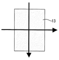
【解決手段】 複数ノズルを有するインクジェットヘッド11、膜形成材料を塗布する薄板状対象物13を吸着保持することができるステージ12、各インクジェットノズルの間欠吐出を制御することができる制御部、及び、膜形成材料を貯蔵しておくタンク部等からなる基本構成を有する膜形成装置であって、上記膜形成装置は、インクジェットヘッド11及び/又はステージ12が移動可能で、かつステージ12が±180°の旋回が可能で、ステージ12に吸着保持された薄板状対象物13の投入方向を任意に変更させることができる膜形成装置。
【選択図】 図1
PROBLEM TO BE SOLVED: To provide a film forming apparatus capable of forming a uniform thin film by preventing drying unevenness and coating unevenness caused by the surface shape and surface material of an object, and a film forming method using the same. provide.
An inkjet head having a plurality of nozzles, a stage capable of adsorbing and holding a thin plate-like object to which a film forming material is applied, a control unit capable of controlling intermittent ejection of each inkjet nozzle, and A film forming apparatus having a basic configuration comprising a tank unit or the like for storing a film forming material, wherein the film forming apparatus is capable of moving the inkjet head 11 and / or the stage 12 and the stage 12 is ± 180 °. The film forming apparatus can freely change the direction in which the thin plate-like object 13 sucked and held on the stage 12 is placed.
[Selection] Figure 1
Description
本発明は、膜形成装置及び膜形成方法に関する。より詳しくは、液晶表示装置に用いられる基板上に配向膜を形成させるのに好適に用いることができるインクジェット方式の膜形成装置、及び、それを用いた膜形成方法に関するものである。 The present invention relates to a film forming apparatus and a film forming method. More specifically, the present invention relates to an ink jet film forming apparatus that can be suitably used to form an alignment film on a substrate used in a liquid crystal display device, and a film forming method using the same.
膜形成装置は、液晶表示装置に用いられる基板等の対象物上に膜を形成させるための装置であり、例えば、インクジェット方式により対象物上に液状の膜形成材料を付着させる膜形成装置が知られている(例えば、特許文献1〜4参照。)。このようなインクジェット方式により液状の膜形成材料を塗布する場合、インクジェットノズルより吐出された膜形成材料は、対象物上に着弾した後、液滴(ドット)が広がりながら乾燥していくこととなるが、インクジェット方式では、通常揮発性の高い膜形成材料が使用されるため、微妙な塗布タイミングの間隔により、ドット間の界面でムラが生じ易く、この点において工夫の余地があった。
例えば、従来のインクジェット方式による膜形成装置においては、通常ノズル間隔(ピッチ)が数百μm離れているため、ノズルピッチの1/2、1/3又は1/4と塗布位置をずらしながら、移動吐出(走査)を繰り返してドットを繋げており、これに起因して走査方向に筋状の乾燥ムラが生じ易く、例えば、液晶表示装置を構成する基板上に配向膜を形成した場合においては、それが液晶表示装置における表示ムラとして認識されていた。
また、従来のインクジェット方式においては、インクジェットノズルより吐出された膜形成材料は、板状対象物上に着弾した後、フラットな板状対象物上であれば、規則正しく円形状に広がり、ドットが繋がりながら整列していくが、例えば、アレイ基板(TFT等のアクティブ素子が形成された基板)、カラーフィルタ基板等の配線やパターンによる段差のある基板では、着弾位置によりドットの広がり形状が不規則となるため、ドットが繋がらないことがあり、繋がってもムラが生じやすかった。
For example, in a conventional ink-jet type film forming apparatus, the nozzle spacing (pitch) is usually several hundred μm apart, so the nozzle position moves while shifting the coating position to 1/2, 1/3, or 1/4. Dots are connected by repeating discharge (scanning), and due to this, streaky drying unevenness is likely to occur in the scanning direction.For example, in the case where an alignment film is formed on a substrate constituting a liquid crystal display device, This was recognized as display unevenness in the liquid crystal display device.
In the conventional ink jet method, the film forming material discharged from the ink jet nozzle is landed on the plate-like object, and then spreads regularly in a circular shape on the flat plate-like object, and dots are connected. For example, in the case of an array substrate (a substrate on which an active element such as a TFT is formed) or a substrate having a step due to a pattern such as a color filter substrate, the dot spreading shape is irregular depending on the landing position. Therefore, the dots may not be connected, and even if they are connected, unevenness is likely to occur.
本発明は、上記現状に鑑みてなされたものであり、対象物の表面形状や表面材質等に起因して発生する乾燥ムラ、塗布ムラが防止され、均一な薄膜を形成することができる膜形成装置、及び、それを用いた膜形成方法を提供することを目的とするものである。 The present invention has been made in view of the above-described present situation, and is capable of forming a uniform thin film by preventing drying unevenness and coating unevenness caused by the surface shape and surface material of an object. It is an object of the present invention to provide an apparatus and a film forming method using the same.
本発明者らは、インクジェット方式を用いた膜形成装置及び膜形成方法について種々検討するうち、ステージとインクジェットノズルとの配置関係が限定されているために、対象物に対するインクジェットノズルの走査方向が限定されていることに着目した。そして、走査方向を任意に変更可能にすることで、対象物の表面形状や表面材質等に応じて個別に走査方向を調整することができ、均一な薄膜を形成することが可能となることを見いだし、上記課題をみごとに解決することができることに想到し、本発明に到達したものである。 The inventors of the present invention have variously studied the film forming apparatus and the film forming method using the ink jet method, and the arrangement relationship between the stage and the ink jet nozzle is limited. Therefore, the scanning direction of the ink jet nozzle with respect to the object is limited. Focused on what has been done. And by making it possible to arbitrarily change the scanning direction, the scanning direction can be individually adjusted according to the surface shape, surface material, etc. of the object, and a uniform thin film can be formed. As a result, the inventors have arrived at the present invention by conceiving that the above problems can be solved brilliantly.
すなわち本発明は、複数ノズルを有するインクジェットヘッドと、膜形成材料を塗布する対象物を載置するステージとを備えた膜形成装置であって、上記膜形成装置は、インクジェットヘッド及び/又はステージが移動し、かつステージが360°旋回する機構を有する膜形成装置である。
以下に本発明を詳述する。
That is, the present invention is a film forming apparatus including an ink jet head having a plurality of nozzles and a stage on which an object to be coated with a film forming material is placed. The film forming apparatus includes an ink jet head and / or a stage. This is a film forming apparatus having a mechanism that moves and a stage rotates 360 °.
The present invention is described in detail below.
本発明の膜形成装置は、複数ノズルを有するインクジェットヘッドと、膜形成材料を塗布する対象物を載置するステージとを備えたものである。インクジェットヘッドとしては、複数のノズルから膜形成材料を吐出させることができるものであれば特に限定されず、ピエゾ方式、サーマルインクジェット方式等の吐出方式により膜形成材料を吐出させるものが挙げられる。なお、ピエゾ方式は、電圧を印加すると変形するピエゾ素子を用いて材料を押し出させる方式であり、サーマルインクジェット方式は、発熱体により気泡を発生させて圧力を加え、材料を吐出させる方式である。ステージとしては、膜形成材料を塗布する対象物を載置することができるものであれば特に限定されないが、上面(対象物の載置面)が平坦であることが好ましい。 The film forming apparatus of the present invention includes an inkjet head having a plurality of nozzles, and a stage on which an object to be coated with a film forming material is placed. The inkjet head is not particularly limited as long as the film forming material can be discharged from a plurality of nozzles, and examples thereof include those that discharge the film forming material by a discharging method such as a piezo method or a thermal ink jet method. Note that the piezo method is a method in which a material is pushed out using a piezo element that deforms when a voltage is applied, and the thermal ink jet method is a method in which bubbles are generated by a heating element, pressure is applied, and the material is discharged. The stage is not particularly limited as long as an object to which the film forming material is applied can be placed, but the upper surface (the object placement surface) is preferably flat.
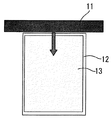
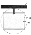
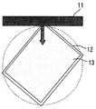
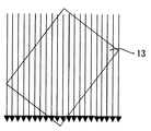
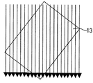
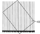
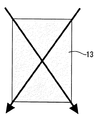
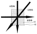
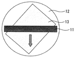
上記膜形成装置は、インクジェットヘッド及び/又はステージが移動し、かつステージが360°旋回する機構を有する。なお、本発明において、360°旋回可能であるとは、一方の回転方向に向けて360°旋回可能な形態であってもよく、一方の回転方向に向けてX°旋回可能であり、かつ他方の回転方向に向けて(360−X)°旋回可能な形態であってもよい。このような膜形成装置においては、インクジェットヘッド及び/又はステージが移動するように構成されていることにより、インクジェットヘッドとステージとの位置関係を変化させながら、インクジェット方式による膜形成材料の塗布を並行して行い、ステージ上に載置された対象物の全面又は所望の位置に膜を形成させることができる。また、ステージが360°旋回するように構成されていることにより、インクジェットヘッドとステージとの角度を任意に変更させて、対象物に対するインクジェットヘッドの走査方向、すなわち対象物に対する膜形成材料の塗布方向を任意に設定することが容易に可能である。これについて、図2〜4を参照して説明すると、ステージ12を回転させることにより、インクジェットヘッド11に対してステージ12の長手方向を縦方向(図2−a)、横方向(図3−a)、斜め方向(図4−a)に向け、その状態で、図2−a、3−a、4−a中の矢印方向に沿ってインクジェットヘッド11を移動させながら塗布を行うことにより、図2−b、3−b、4−b中の矢印方向に沿って膜形成材料が対象物13上に塗布されていくこととなる。このように膜形成材料の塗布方向を任意に設定することができると、対象物の表面形状や表面材質等の表面状態に応じて、膜形成材料の塗布方向を調整することができるので、塗布方向に発生する筋状の乾燥ムラや塗布ムラを低減して、均一な薄膜を形成させることが可能となる。
The film forming apparatus has a mechanism in which the inkjet head and / or the stage moves and the stage rotates 360 °. In the present invention, being 360 ° turnable may be a form capable of 360 ° turn in one rotation direction, X ° turn in one rotation direction, and the other (360-X) may be possible to turn in the direction of rotation. In such a film forming apparatus, the inkjet head and / or the stage is configured to move, so that the application of the film forming material by the inkjet method is performed in parallel while changing the positional relationship between the inkjet head and the stage. Thus, a film can be formed on the entire surface of the object placed on the stage or at a desired position. Further, since the stage is configured to rotate 360 °, the angle between the inkjet head and the stage is arbitrarily changed, and the scanning direction of the inkjet head with respect to the object, that is, the coating direction of the film forming material with respect to the object Can be easily set. This will be described with reference to FIGS. 2 to 4. By rotating the
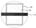
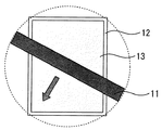
また、本発明においては、対象物に対するインクジェットノズルの走査方向を任意に変更することが容易に可能であることから、対象物に対して2以上の異なる方向から膜形成材料を重ね塗りすることも容易に可能である。これについて、図5、6を参照して説明すると、インクジェットヘッド11に対してステージ12の長手方向を斜め方向(図5−a)、縦方向(図6−a)に向けた状態で、図5−a、6−a中の矢印方向に沿って1度目の塗布を行った後、ステージ12を回転させ、斜め方向(図5−b)、横方向(図6−b)に向け直した状態で、図5−b、6−b中の矢印方向に沿って2度目の塗布を行うことにより、図5−c、図6−c中の矢印で示すように、膜形成材料の塗布方向を交差させた重ね塗りが可能となる。このような重ね塗りは、インクジェットヘッドの吐出条件によっては、均一な薄膜を形成させるための有効な手法となり得るものである。
In the present invention, since the scanning direction of the ink jet nozzle with respect to the object can be easily changed arbitrarily, the film forming material can be overcoated from two or more different directions on the object. Easily possible. This will be described with reference to FIGS. 5 and 6 in a state in which the longitudinal direction of the
上記ステージは、膜形成材料を塗布する対象物を吸着保持する機構を有するものであることが好ましい。このような形態においては、ステージの構成が簡単であるとともに、ステージ上に対象物を充分に固定することができるので、対象物上に精度よく膜形成材料を付着させ、均一な薄膜を形成させることができる。吸着保持機構の好ましい形態としては、真空吸着を行うものが挙げられる。 The stage preferably has a mechanism for adsorbing and holding an object to which the film forming material is applied. In such a form, the structure of the stage is simple and the object can be sufficiently fixed on the stage, so that the film-forming material is attached to the object with high precision and a uniform thin film is formed. be able to. A preferable form of the suction holding mechanism is one that performs vacuum suction.
本発明の膜形成装置の構成としては、このような構成要素を必須として形成されるものである限り、その他の構成要素を含んでいても含んでいなくてもよく、特に限定されるものではない。また、本発明において、膜塗布材料としては特に限定されるものではないが、インクジェット方式により塗布するのに適した特性を有するものが好ましく、例えば、揮発性材料を含有する液状材料等が好適である。膜形成材料を塗布する対象物としては特に限定されるものではないが、液晶表示装置を構成するアレイ基板やカラーフィルタ基板等が好適である。これらの基板においては、配線やパターンによる段差が存在するため、乾燥ムラ、塗布ムラが発生しやすく、本発明の作用効果を充分に得ることができる。 The structure of the film forming apparatus of the present invention is not particularly limited as long as such a component is formed as essential, and may or may not include other components. Absent. Further, in the present invention, the film coating material is not particularly limited, but preferably has a characteristic suitable for coating by an ink jet method, for example, a liquid material containing a volatile material is suitable. is there. The object to which the film forming material is applied is not particularly limited, but an array substrate, a color filter substrate, or the like that constitutes the liquid crystal display device is preferable. In these substrates, since there are steps due to wiring and patterns, drying unevenness and coating unevenness are likely to occur, and the effects of the present invention can be sufficiently obtained.
本発明はまた、上記膜形成装置を用いて膜形成材料を対象物に塗布する膜形成方法であって、上記膜形成方法は、膜形成材料を塗布する対象物に対するインクジェットヘッドの走査方向を調整して塗布する工程を含む膜形成方法でもある。このような膜形成方法によれば、対象物に対するインクジェットヘッドの走査方向(膜形成材料の塗布方向)を、対象物の表面形状や表面材質等の表面状態に応じて調整することで、膜形成材料の塗布方向に発生する筋状の乾燥ムラや塗布ムラを低減して、対象物上に均一な薄膜を形成することが可能であり、例えば、液晶表示装置を構成するアレイ基板やカラーフィルタ基板等に対して配向膜の材料を塗布するのに好適である。また、塗布工程は、膜形成材料を塗布する対象物に対して2以上の異なる方向から重ね塗りを行う工程であることが好ましい。このような塗布形態は、インクジェットヘッドの吐出条件によっては、均一な薄膜を形成させるための有効な手法となり得るものである。 The present invention is also a film forming method in which a film forming material is applied to an object using the film forming apparatus, and the film forming method adjusts the scanning direction of the inkjet head relative to the object to which the film forming material is applied. It is also a film forming method including a coating step. According to such a film formation method, the film formation is performed by adjusting the scanning direction of the ink jet head (the application direction of the film formation material) with respect to the object according to the surface state of the object such as the surface shape and surface material. It is possible to reduce streaky drying unevenness and application unevenness that occur in the material application direction and form a uniform thin film on an object. For example, an array substrate or a color filter substrate constituting a liquid crystal display device It is suitable for applying the material of the alignment film to the same. Moreover, it is preferable that an application | coating process is a process of performing the overcoat from the 2 or more different direction with respect to the target object which apply | coats film forming material. Such a coating form can be an effective method for forming a uniform thin film depending on the discharge conditions of the inkjet head.
本発明の膜形成装置によれば、インクジェットヘッド及び/又はステージが移動し、かつステージが360°旋回する機構を有することから、膜形成材料を塗布する対象物の表面形状や表面材質等の表面状態に応じて、対象物に対する材料の塗布方向を容易に調整することができ、塗布方向に発生する筋状の乾燥ムラや塗布ムラを低減して、均一な薄膜を形成させることが可能となる。また、対象物に対して2以上の異なる方向から材料を重ね塗りすることも容易に可能となり、これによっても均一な薄膜を形成させることが可能となる。 According to the film forming apparatus of the present invention, since the inkjet head and / or the stage moves and the stage has a mechanism that rotates 360 °, the surface such as the surface shape or surface material of the object to which the film forming material is applied The application direction of the material to the object can be easily adjusted according to the state, and it becomes possible to reduce the streaky drying unevenness and application unevenness generated in the application direction and form a uniform thin film. . Further, it is possible to easily apply the material to the object from two or more different directions, and it is also possible to form a uniform thin film.
以下に実施例を掲げ、本発明を図面に基づいて更に詳細に説明するが、本発明はこれらの実施例のみに限定されるものではない。 EXAMPLES Although an Example is hung up below and this invention is demonstrated still in detail based on drawing, this invention is not limited only to these Examples.
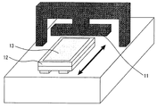
(実施例1)
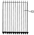
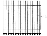
図1は、本発明の膜形成装置の構成の一例を示す斜視模式図である。
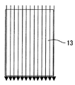
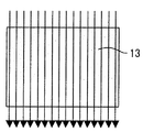
図1に示す膜形成装置は、材料の射出口となるインクジェットノズルを複数個直列又は千鳥配列に配置して大面積の塗布を可能にしたインクジェットヘッド11と、移動及び360°(±180°)の旋回が可能であり、かつ吸着保持機構を備えるステージ12と、インクジェットノズルからの材料の間欠吐出を制御することができる制御部(図示せず)と、材料を貯蔵することができるタンク部(図示せず)とを有している。
(Example 1)
FIG. 1 is a schematic perspective view showing an example of the configuration of the film forming apparatus of the present invention.
The film forming apparatus shown in FIG. 1 includes an
本実施例においては、液晶表示装置の製造に用いられる配向膜材料の塗布による薄膜形成について以下に説明する。
まず、インクジェットヘッド11をステージ12の走査方向と直交する状態にて設置した。次に、薄板状対象物(以下、基板ともいう)13として、50mm×50mmの5種のアレイ基板、4種のカラーフィルタ基板、ITO全面デポ基板(酸化インジウム錫膜を全面に形成した基板)をステージ12上に搭載させた。基板13としては、UV(波長:172nm)洗浄後、純水又はアルコール洗浄を行ったものを用いた。基板13搭載後、真空吸着にて基板13を保持し、条件毎に吐出方向が異なるようにステージ12の角度を調整した。なお、本実施例では、図7に示すように、縦方向(A方向)、横方向(B方向)、斜め方向(C方向)の3方向の塗布方向について、成膜状態の確認を行った。
In this embodiment, a thin film formation by applying an alignment film material used for manufacturing a liquid crystal display device will be described below.
First, the
このようにして塗布の準備が整ったところで、ステージ12を直線方向(図1中の矢印方向)に走査させ、それと同期させてインクジェットノズルより配向膜材料を吐出させた。配向膜材料としては、フレキソ印刷グレード品を希釈し、固形分濃度1〜3質量%、粘度3.5〜12mPa・sに調整したものを用いた。吐出のON、OFFのタイミングとしては、1秒間に300〜1000回程度とし、所望のドット密度に合わせるためにステージ12の走査速度を調整した。すなわち、走査方向の塗布ピッチは、基本的にノズルピッチと等間隔にしたが、膜厚調整を行う場合には、塗布ピッチを調整した。また、基板13上に形成されている配線部の段差や金属膜面等の状況により、配向膜材料の液滴の流動状態が変化するため、その対策として、各基板13に応じて吐出量やステージ12の走査速度を変化させ、所望の配向膜厚(60〜100nm)にコントロールした。
When preparation for coating was completed in this way, the
以上の条件にて配向膜材料を成膜させた基板13をステージ12より離脱させた後、ヒータ部に搭載し、60〜80℃で乾燥処理を行った。そして、配向膜材料の乾燥後に、基板13を処理部から移動させ、パネル評価を行った。パネル評価の評価基準としては、成膜状態が良好であったものを○とし、成膜状態にムラが有ったものを△とし、成膜状態が悪かったものを×とした。その結果を表1に示す。
After the

表1に示すように、基板や機種毎に成膜状態の良好な走査方向が存在することが判明した。従って、良好な成膜状態を得るためには、基板や機種毎にステージ12の走査方向を設定する必要があり、そのための手段として、本発明に係るステージ12が360°旋回する機構が非常に有効な手段であることが分かった。
As shown in Table 1, it has been found that there is a good scanning direction of the film formation state for each substrate and model. Therefore, in order to obtain a good film formation state, it is necessary to set the scanning direction of the
(比較例1)
インクジェットヘッドの走査方向を変更可能とするために、図8−a及び8−bに示すように、上部のインクジェットヘッド11を旋回かつ走査可能にした形態においては、インクジェットヘッド11の駆動部が大型化してしまうというデメリットを有するため、実際の設備としては不向きである。
(Comparative Example 1)
In order to make the scanning direction of the inkjet head changeable, as shown in FIGS. 8A and 8B, in the form in which the
(比較例2)
インクジェットヘッドの走査方向を変更可能とするために、図9−aに示すように、ロボットハンド20にて基板13の投入方向を変更可能にしたり、ステージ12の上流側ポジションに旋回可能な置台を設け、これにより基板13を旋回させてからロボットにてステージ12に投入したりすることで、ステージ12上の基板13の位置を変更可能にした形態においては、図9−bに示すように、全方向の保持を可能とするためにステージ12が大型化してしまうことに加え、吐出走査方向を交差させて重ね塗りするという手段が得られなくなってしまうというデメリットを有する。なお、比較例2の形態においても、同じ方向に重ね塗りをすることは可能であるが、違う方向にて重ね塗りを行う場合(交差させて重ね塗りをする場合)には、ステージ側が1軸しか動作できないため、ステージに吸着させた基板に対して、インクジェットヘッドの方を旋回させて違う方向から塗布動作を行うか、一度基板をステージから離脱させて、もう一度違う方向に吸着させて処理を行うかする必要がある。
(Comparative Example 2)
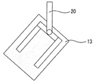
In order to be able to change the scanning direction of the inkjet head, as shown in FIG. 9A, the loading direction of the
11:インクジェットヘッド
12:ステージ
13:対象物(基板)
20:ロボットハンド
11: Inkjet head 12: Stage 13: Object (substrate)
20: Robot hand
Claims (4)
該膜形成装置は、インクジェットヘッド及び/又はステージが移動し、かつステージが360°旋回する機構を有することを特徴とする膜形成装置。 A film forming apparatus comprising an inkjet head having a plurality of nozzles and a stage on which an object to be coated with a film forming material is placed,
The film forming apparatus has a mechanism in which an inkjet head and / or a stage moves and the stage rotates 360 °.
該膜形成方法は、膜形成材料を塗布する対象物に対するインクジェットヘッドの走査方向を調整して塗布する工程を含むことを特徴とする膜形成方法。 A film forming method for applying a film forming material to an object using the film forming apparatus according to claim 1,
The film forming method includes a step of applying the film forming material by adjusting the scanning direction of the ink jet head with respect to an object to which the film forming material is applied.
Priority Applications (1)
| Application Number | Priority Date | Filing Date | Title |
|---|---|---|---|
| JP2004118329A JP2005296854A (en) | 2004-04-13 | 2004-04-13 | Film forming apparatus and film forming method |
Applications Claiming Priority (1)
| Application Number | Priority Date | Filing Date | Title |
|---|---|---|---|
| JP2004118329A JP2005296854A (en) | 2004-04-13 | 2004-04-13 | Film forming apparatus and film forming method |
Publications (1)
| Publication Number | Publication Date |
|---|---|
| JP2005296854A true JP2005296854A (en) | 2005-10-27 |
Family
ID=35329047
Family Applications (1)
| Application Number | Title | Priority Date | Filing Date |
|---|---|---|---|
| JP2004118329A Pending JP2005296854A (en) | 2004-04-13 | 2004-04-13 | Film forming apparatus and film forming method |
Country Status (1)
| Country | Link |
|---|---|
| JP (1) | JP2005296854A (en) |
Cited By (14)
| Publication number | Priority date | Publication date | Assignee | Title |
|---|---|---|---|---|
| JP2005193232A (en) * | 2003-12-12 | 2005-07-21 | Shibaura Mechatronics Corp | Coating apparatus and coating method |
| WO2006118089A1 (en) * | 2005-04-28 | 2006-11-09 | Shibaura Mechatronics Corporation | Solution application device and solution application method |
| JP2007237162A (en) * | 2006-02-13 | 2007-09-20 | Seiko Epson Corp | Pattern formation method, alignment film formation method, droplet discharge device, alignment film formation device, electro-optical device, and liquid crystal display device |
| JP2007313439A (en) * | 2006-05-26 | 2007-12-06 | Hitachi High-Technologies Corp | Resin coating apparatus and resin coating method |
| JP2008068190A (en) * | 2006-09-13 | 2008-03-27 | Ricoh Printing Systems Ltd | Liquid droplet discharging method |
| WO2009072327A1 (en) * | 2007-12-05 | 2009-06-11 | Sharp Kabushiki Kaisha | Display element |
| WO2011118652A1 (en) * | 2010-03-26 | 2011-09-29 | シャープ株式会社 | Film forming apparatus and film forming method |
| JP2012053395A (en) * | 2010-09-03 | 2012-03-15 | Hitachi Displays Ltd | Manufacturing method of display device |
| JP2013079408A (en) * | 2011-09-30 | 2013-05-02 | Dainippon Printing Co Ltd | Copper particulate dispersion, method for forming pattern and method for manufacturing copper pattern film |
| JPWO2013089049A1 (en) * | 2011-12-14 | 2015-04-27 | 住友重機械工業株式会社 | Touch panel manufacturing method and substrate manufacturing apparatus |
| JP2015131261A (en) * | 2014-01-10 | 2015-07-23 | 株式会社石井表記 | Film forming device and film forming method |
| WO2015155953A1 (en) * | 2014-04-10 | 2015-10-15 | 株式会社Joled | Organic el display panel production method |
| KR101759132B1 (en) | 2008-03-31 | 2017-07-18 | 도레 엔지니아린구 가부시키가이샤 | Coating machine and coating method |
| WO2018198303A1 (en) * | 2017-04-28 | 2018-11-01 | シャープ株式会社 | Application device, and device and method for producing electronic device |
-
2004
- 2004-04-13 JP JP2004118329A patent/JP2005296854A/en active Pending
Cited By (27)
| Publication number | Priority date | Publication date | Assignee | Title |
|---|---|---|---|---|
| JP2005193232A (en) * | 2003-12-12 | 2005-07-21 | Shibaura Mechatronics Corp | Coating apparatus and coating method |
| WO2006118089A1 (en) * | 2005-04-28 | 2006-11-09 | Shibaura Mechatronics Corporation | Solution application device and solution application method |
| JPWO2006118089A1 (en) * | 2005-04-28 | 2008-12-18 | 芝浦メカトロニクス株式会社 | Solution coating apparatus and coating method |
| JP2010005619A (en) * | 2005-04-28 | 2010-01-14 | Shibaura Mechatronics Corp | Apparatus and method for application of solution |
| JP4538002B2 (en) * | 2005-04-28 | 2010-09-08 | 芝浦メカトロニクス株式会社 | Solution coating apparatus and coating method |
| JP2007237162A (en) * | 2006-02-13 | 2007-09-20 | Seiko Epson Corp | Pattern formation method, alignment film formation method, droplet discharge device, alignment film formation device, electro-optical device, and liquid crystal display device |
| US7816277B2 (en) | 2006-02-13 | 2010-10-19 | Seiko Epson Corporation | Method for forming deposit, droplet ejection apparatus, electro-optic device, and liquid crystal display |
| JP2007313439A (en) * | 2006-05-26 | 2007-12-06 | Hitachi High-Technologies Corp | Resin coating apparatus and resin coating method |
| JP2008068190A (en) * | 2006-09-13 | 2008-03-27 | Ricoh Printing Systems Ltd | Liquid droplet discharging method |
| WO2009072327A1 (en) * | 2007-12-05 | 2009-06-11 | Sharp Kabushiki Kaisha | Display element |
| CN101889242B (en) * | 2007-12-05 | 2013-04-17 | 夏普株式会社 | Display element and manufacture method thereof |
| KR101759132B1 (en) | 2008-03-31 | 2017-07-18 | 도레 엔지니아린구 가부시키가이샤 | Coating machine and coating method |
| CN102821869A (en) * | 2010-03-26 | 2012-12-12 | 夏普株式会社 | Film forming apparatus and film forming method |
| WO2011118652A1 (en) * | 2010-03-26 | 2011-09-29 | シャープ株式会社 | Film forming apparatus and film forming method |
| JP5492289B2 (en) * | 2010-03-26 | 2014-05-14 | シャープ株式会社 | Film forming apparatus and film forming method |
| CN102821869B (en) * | 2010-03-26 | 2015-06-24 | 夏普株式会社 | Film forming apparatus and film forming method |
| JP2012053395A (en) * | 2010-09-03 | 2012-03-15 | Hitachi Displays Ltd | Manufacturing method of display device |
| JP2013079408A (en) * | 2011-09-30 | 2013-05-02 | Dainippon Printing Co Ltd | Copper particulate dispersion, method for forming pattern and method for manufacturing copper pattern film |
| JPWO2013089049A1 (en) * | 2011-12-14 | 2015-04-27 | 住友重機械工業株式会社 | Touch panel manufacturing method and substrate manufacturing apparatus |
| TWI594804B (en) * | 2011-12-14 | 2017-08-11 | Sumitomo Heavy Industries | Touch panel manufacturing method |
| JP2015131261A (en) * | 2014-01-10 | 2015-07-23 | 株式会社石井表記 | Film forming device and film forming method |
| WO2015155953A1 (en) * | 2014-04-10 | 2015-10-15 | 株式会社Joled | Organic el display panel production method |
| CN106165542A (en) * | 2014-04-10 | 2016-11-23 | 株式会社日本有机雷特显示器 | Manufacturing method of organic EL display panel |
| JPWO2015155953A1 (en) * | 2014-04-10 | 2017-04-13 | 株式会社Joled | Manufacturing method of organic EL display panel |
| US10541367B2 (en) | 2014-04-10 | 2020-01-21 | Joled Inc. | Organic EL display panel production method |
| WO2018198303A1 (en) * | 2017-04-28 | 2018-11-01 | シャープ株式会社 | Application device, and device and method for producing electronic device |
| US10305038B1 (en) | 2017-04-28 | 2019-05-28 | Sharp Kabushiki Kaisha | Manufacturing method |
Similar Documents
| Publication | Publication Date | Title |
|---|---|---|
| JP2005296854A (en) | Film forming apparatus and film forming method | |
| US9343339B2 (en) | Coating method and coating apparatus | |
| CN101616805B (en) | Cleaning method for ink-jet coating device | |
| CN115837805B (en) | Device for realizing ink jet printing on side edge of display panel and ink jet printing control method thereof | |
| JP5244758B2 (en) | Solution coating apparatus and coating method | |
| TW200800627A (en) | Method and apparatus for printing | |
| JP2008544333A (en) | Inkjet printing system and method for flat panel display | |
| US11376847B2 (en) | Liquid droplet ejection device and liquid droplet ejection method | |
| JP2010005619A5 (en) | ||
| TWI741426B (en) | Coating device and coating method | |
| JP2006088070A (en) | Inkjet coating method and display device manufacturing method | |
| JP5693943B2 (en) | Alignment film forming liquid coating apparatus and alignment film forming substrate manufacturing method | |
| CN100538458C (en) | Inkjet alignment layer printing apparatus and printing method | |
| JP2019130447A (en) | Film formation method, film formation device and composite substrate of forming film | |
| TW201334982A (en) | Inkjet coating device and inkjet coating method | |
| JP4627618B2 (en) | Film forming method and film forming apparatus | |
| JP4202278B2 (en) | Method for forming alignment film | |
| JP2019109573A (en) | Film formation apparatus and film formation method | |
| JP2008296122A (en) | Method for forming thin film using liquid material | |
| CN1536414A (en) | Solution coating device and coating method | |
| TWI398358B (en) | Color filter manufacturing method and device thereof | |
| CN101889242A (en) | Display element | |
| JP4165100B2 (en) | Droplet ejection apparatus, droplet ejection method, device manufacturing apparatus, device manufacturing method, and device | |
| CN1707335A (en) | Alignment film forming apparatus, alignment film forming method, drawing apparatus, and drawing method | |
| JP2006289322A (en) | Combined inkjet head |