JP2005294851A - Low temperature polysilicon TFT structure and method of manufacturing channel layer thereof - Google Patents
Low temperature polysilicon TFT structure and method of manufacturing channel layer thereof Download PDFInfo
- Publication number
- JP2005294851A JP2005294851A JP2005108557A JP2005108557A JP2005294851A JP 2005294851 A JP2005294851 A JP 2005294851A JP 2005108557 A JP2005108557 A JP 2005108557A JP 2005108557 A JP2005108557 A JP 2005108557A JP 2005294851 A JP2005294851 A JP 2005294851A
- Authority
- JP
- Japan
- Prior art keywords
- layer
- thin film
- low
- region
- temperature polysilicon
- Prior art date
- Legal status (The legal status is an assumption and is not a legal conclusion. Google has not performed a legal analysis and makes no representation as to the accuracy of the status listed.)
- Pending
Links
Images


Classifications
-
- H—ELECTRICITY
- H10—SEMICONDUCTOR DEVICES; ELECTRIC SOLID-STATE DEVICES NOT OTHERWISE PROVIDED FOR
- H10D—INORGANIC ELECTRIC SEMICONDUCTOR DEVICES
- H10D30/00—Field-effect transistors [FET]
- H10D30/60—Insulated-gate field-effect transistors [IGFET]
- H10D30/67—Thin-film transistors [TFT]
- H10D30/6729—Thin-film transistors [TFT] characterised by the electrodes
- H10D30/673—Thin-film transistors [TFT] characterised by the electrodes characterised by the shapes, relative sizes or dispositions of the gate electrodes
- H10D30/6733—Multi-gate TFTs
-
- H—ELECTRICITY
- H10—SEMICONDUCTOR DEVICES; ELECTRIC SOLID-STATE DEVICES NOT OTHERWISE PROVIDED FOR
- H10D—INORGANIC ELECTRIC SEMICONDUCTOR DEVICES
- H10D30/00—Field-effect transistors [FET]
- H10D30/01—Manufacture or treatment
- H10D30/021—Manufacture or treatment of FETs having insulated gates [IGFET]
- H10D30/031—Manufacture or treatment of FETs having insulated gates [IGFET] of thin-film transistors [TFT]
- H10D30/0312—Manufacture or treatment of FETs having insulated gates [IGFET] of thin-film transistors [TFT] characterised by the gate electrodes
- H10D30/0314—Manufacture or treatment of FETs having insulated gates [IGFET] of thin-film transistors [TFT] characterised by the gate electrodes of lateral top-gate TFTs comprising only a single gate
-
- H—ELECTRICITY
- H10—SEMICONDUCTOR DEVICES; ELECTRIC SOLID-STATE DEVICES NOT OTHERWISE PROVIDED FOR
- H10D—INORGANIC ELECTRIC SEMICONDUCTOR DEVICES
- H10D30/00—Field-effect transistors [FET]
- H10D30/01—Manufacture or treatment
- H10D30/021—Manufacture or treatment of FETs having insulated gates [IGFET]
- H10D30/031—Manufacture or treatment of FETs having insulated gates [IGFET] of thin-film transistors [TFT]
- H10D30/0321—Manufacture or treatment of FETs having insulated gates [IGFET] of thin-film transistors [TFT] comprising silicon, e.g. amorphous silicon or polysilicon
-
- H—ELECTRICITY
- H10—SEMICONDUCTOR DEVICES; ELECTRIC SOLID-STATE DEVICES NOT OTHERWISE PROVIDED FOR
- H10D—INORGANIC ELECTRIC SEMICONDUCTOR DEVICES
- H10D30/00—Field-effect transistors [FET]
- H10D30/60—Insulated-gate field-effect transistors [IGFET]
- H10D30/67—Thin-film transistors [TFT]
- H10D30/6729—Thin-film transistors [TFT] characterised by the electrodes
- H10D30/673—Thin-film transistors [TFT] characterised by the electrodes characterised by the shapes, relative sizes or dispositions of the gate electrodes
- H10D30/6731—Top-gate only TFTs
-
- H—ELECTRICITY
- H10—SEMICONDUCTOR DEVICES; ELECTRIC SOLID-STATE DEVICES NOT OTHERWISE PROVIDED FOR
- H10D—INORGANIC ELECTRIC SEMICONDUCTOR DEVICES
- H10D30/00—Field-effect transistors [FET]
- H10D30/60—Insulated-gate field-effect transistors [IGFET]
- H10D30/67—Thin-film transistors [TFT]
- H10D30/674—Thin-film transistors [TFT] characterised by the active materials
- H10D30/6741—Group IV materials, e.g. germanium or silicon carbide
- H10D30/6743—Silicon
- H10D30/6745—Polycrystalline or microcrystalline silicon
-
- H—ELECTRICITY
- H10—SEMICONDUCTOR DEVICES; ELECTRIC SOLID-STATE DEVICES NOT OTHERWISE PROVIDED FOR
- H10D—INORGANIC ELECTRIC SEMICONDUCTOR DEVICES
- H10D30/00—Field-effect transistors [FET]
- H10D30/60—Insulated-gate field-effect transistors [IGFET]
- H10D30/67—Thin-film transistors [TFT]
- H10D30/6757—Thin-film transistors [TFT] characterised by the structure of the channel, e.g. transverse or longitudinal shape or doping profile
-
- H—ELECTRICITY
- H10—SEMICONDUCTOR DEVICES; ELECTRIC SOLID-STATE DEVICES NOT OTHERWISE PROVIDED FOR
- H10D—INORGANIC ELECTRIC SEMICONDUCTOR DEVICES
- H10D62/00—Semiconductor bodies, or regions thereof, of devices having potential barriers
- H10D62/40—Crystalline structures
-
- H—ELECTRICITY
- H10—SEMICONDUCTOR DEVICES; ELECTRIC SOLID-STATE DEVICES NOT OTHERWISE PROVIDED FOR
- H10D—INORGANIC ELECTRIC SEMICONDUCTOR DEVICES
- H10D86/00—Integrated devices formed in or on insulating or conducting substrates, e.g. formed in silicon-on-insulator [SOI] substrates or on stainless steel or glass substrates
- H10D86/01—Manufacture or treatment
- H10D86/021—Manufacture or treatment of multiple TFTs
- H10D86/0251—Manufacture or treatment of multiple TFTs characterised by increasing the uniformity of device parameters
-
- H—ELECTRICITY
- H10—SEMICONDUCTOR DEVICES; ELECTRIC SOLID-STATE DEVICES NOT OTHERWISE PROVIDED FOR
- H10P—GENERIC PROCESSES OR APPARATUS FOR THE MANUFACTURE OR TREATMENT OF DEVICES COVERED BY CLASS H10
- H10P34/00—Irradiation with electromagnetic or particle radiation of wafers, substrates or parts of devices
- H10P34/40—Irradiation with electromagnetic or particle radiation of wafers, substrates or parts of devices with high-energy radiation
- H10P34/42—Irradiation with electromagnetic or particle radiation of wafers, substrates or parts of devices with high-energy radiation with electromagnetic radiation, e.g. laser annealing
Landscapes
- Thin Film Transistor (AREA)
- Recrystallisation Techniques (AREA)
Abstract
Description
本発明はTFT構造及びそのチャネル層の製造方法に係り、特に低温ポリシリコンTFT構造及びそのチャネル層の製造方法に係る。 The present invention relates to a TFT structure and a method for manufacturing the channel layer thereof, and more particularly, to a low-temperature polysilicon TFT structure and a method for manufacturing the channel layer.
大部分の電子素子は、素子を駆動するためのスイッチを必要とする。アクティブ駆動の表示素子を例にあげると、通常はTFT(Thin Film Transistor)を駆動スイッチとしている。そして、TFTはチャネル領域の材質により、アモルファスシリコンTFTと、ポリシリコンTFTとに分けられる。ポリシリコンTFTは、アモルファスTFTに比べてその消費電力が小さく且つ電子移動度が大きいので、次第に市場において注目を集めている。 Most electronic devices require a switch to drive the device. Taking an active drive display element as an example, a TFT (Thin Film Transistor) is usually used as a drive switch. The TFT is divided into an amorphous silicon TFT and a polysilicon TFT depending on the material of the channel region. Polysilicon TFTs are attracting increasing attention in the market because they consume less power and have higher electron mobility than amorphous TFTs.
早期のポリシリコンTFTのプロセス温度は摂氏1000度に達するため、基板材質の選択が大幅に限定されていた。然し、近年レーザ技術の発展により、プロセス温度は摂氏600度以下にまで降下し、このプロセスで形成されたポリシリコンTFTは、低温ポリシリコンTFTとも呼ばれる。 Early polysilicon TFT process temperatures reached 1000 degrees Celsius, greatly limiting the choice of substrate material. However, due to the development of laser technology in recent years, the process temperature has dropped to below 600 degrees Celsius, and the polysilicon TFT formed by this process is also called a low temperature polysilicon TFT.
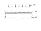
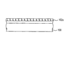
低温ポリシリコンTFTにおいて、ポリシリコン薄膜の形成方法は、先ず基板上にアモルファスシリコン薄膜を形成し、その後アモルファスシリコンを溶融させ、再結晶させてポリシリコン薄膜を形成する。図1A及び図1Bは従来の低温ポリシリコン薄膜の製造フロー断面図である。一般に常用されるレーザアニ−ルプロセス(Laser Annealing Process)はエキシマレーザアニ−ル(Excimer Laser Annealing、以下ELAプロセスという)である。図1Aに示すとおり、基板100上にアモルファスシリコン薄膜102を形成した後、エキシマレーザアニ−ルビーム106によりレーザアニ−ルプロセスを行ってアモルファスシリコン102を溶融させ、図1Bのように、シリコン分子を再結晶させてポリシリコン薄膜102aを形成する。
In a low-temperature polysilicon TFT, a polysilicon thin film is formed by first forming an amorphous silicon thin film on a substrate, and then melting and recrystallizing the amorphous silicon to form a polysilicon thin film. 1A and 1B are cross-sectional views illustrating a manufacturing flow of a conventional low-temperature polysilicon thin film. A laser annealing process generally used is an excimer laser annealing (hereinafter referred to as ELA process). As shown in FIG. 1A, after the amorphous silicon
然しながら、ELAプロセスにより形成されたポリシリコン薄膜102aは、結晶粒の大きさが小さすぎ、且つサイズの均一性(uniformity)が良くないので、ポリシリコン薄膜102aには多くの結晶粒界が存在して、ポリシリコン薄膜102aのチャネル領域における電子の移動度が僅か100〜200cm2/V-secであるので、薄膜トランジスタの機能にかなり大きな影響を与える。 However, since the polysilicon thin film 102a formed by the ELA process has a crystal grain size that is too small and the uniformity of the size is not good, there are many crystal grain boundaries in the polysilicon thin film 102a. Thus, since the mobility of electrons in the channel region of the polysilicon thin film 102a is only 100 to 200 cm 2 / V-sec, the function of the thin film transistor is considerably affected.
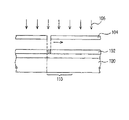
上記の問題を解決するために、従来は逐次的横方向結晶化(Sequential Lateral Solidification, SLS)と呼ばれるレーザアニール工程を提供する。図2A及び2Bは、もう一つの従来の低温ポリシリコン薄膜の製造フロー断面図を示す。 In order to solve the above problem, a laser annealing process conventionally called sequential lateral crystallization (SLS) is provided. 2A and 2B are cross-sectional views illustrating another conventional low-temperature polysilicon thin film manufacturing flow.
図2Aに示すように、SLSプロセスはマスク104でアモルファスシリコン薄膜102がレーザビーム106に照射される範囲を画定して、一部領域内のアモルファスシリコン薄膜102、即ち領域110内のアモルファスシリコン薄膜102を溶融する。あるSLSプロセスにおいて、マスク104は基台により制御されて移動し、レーザビームにマスク104上のホール108を透過させて領域110における全てのアモルファスシリコン薄膜102を照射する。
As shown in FIG. 2A, the SLS process defines a range in which the amorphous silicon
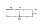
図2Bに示すとおり、一定の時間が経過すると、溶融されたアモルファスシリコン薄膜102(つまり、領域110内のアモルファスシリコン薄膜102)は、溶融していないアモルファスシリコン薄膜102を結晶核として横方向に成長し、領域110内においてポリシリコン薄膜202aを形成する。
As shown in FIG. 2B, after a certain period of time, the molten amorphous silicon thin film 102 (that is, the amorphous silicon
図2Bから分かるように、SLSプロセスにより結晶粒サイズがより大きいポリシリコン薄膜202aを形成することができる。つまり、SLSプロセスにより形成されたポリシリコン薄膜202aにおける結晶粒界が少ないので、SLSプロセスと従来のELAプロセスを比較すると、SLSプロセスはポリシリコン薄膜における電子の移動度を高くするだけでなく、薄膜トランジスタの機能を高めることができ、ポリシリコン薄膜の粒子配向を比較的一致させることができる。 As can be seen from FIG. 2B, the polysilicon thin film 202a having a larger crystal grain size can be formed by the SLS process. In other words, since there are few crystal grain boundaries in the polysilicon thin film 202a formed by the SLS process, comparing the SLS process with the conventional ELA process, the SLS process not only increases the electron mobility in the polysilicon thin film, but also the thin film transistor And the grain orientation of the polysilicon thin film can be made relatively coincident.
然しながら、SLSプロセスで使用する機器設備は比較的高価なもので、従来のELAプロセスに比べ特殊なマスクを余分に使用しなければならないため、トランジスタ全体の製造コストが高くなる。また、SLSプロセスでは、やはりポリシリコン薄膜を形成する所要時間を減少することができない。 However, the equipment used in the SLS process is relatively expensive, and an extra special mask must be used compared to the conventional ELA process, which increases the manufacturing cost of the entire transistor. In addition, in the SLS process, the time required for forming the polysilicon thin film cannot be reduced.
そこで、本発明の目的は低温ポリシリコンTFT構造であって、そのチャネル層における結晶粒がより均一なサイズを有し、且つ結晶粒界がより少なく、トランジスタにより好ましい素子特性をもたせることができる低温ポリシリコンTFT構造を提供する。 Therefore, an object of the present invention is a low-temperature polysilicon TFT structure, in which the crystal grains in the channel layer have a more uniform size, and there are fewer crystal grain boundaries, and the transistor can have favorable device characteristics. A polysilicon TFT structure is provided.
本発明のもう一つの目的は、低温ポリシリコンTFT構造のチャネル層の製造方法を提供し、トランジスタのチャネル領域における結晶粒の大小及びその粒子配向を制御することにより、チャネル領域における電子の移動度を向上させる。この他、該製造方法が使用するプロセス設備は、従来のプロセス設備と相容性があるので、製造コストを節約することができる。 Another object of the present invention is to provide a method for manufacturing a channel layer of a low-temperature polysilicon TFT structure, and by controlling the size of crystal grains in the channel region of the transistor and the grain orientation thereof, the mobility of electrons in the channel region is provided. To improve. In addition, since the process equipment used by the production method is compatible with the conventional process equipment, the production cost can be saved.
上記の目的を達成するために、本発明は、基板上に配置するのに適した低温ポリシリコンTFT構造を提供する。当該低温ポリシリコンTFT構造は、主にキャップ層、ポリシリコン薄膜及びゲートからなる。このうち、キャップ層は基板上方に配置され、基板との間に隙間領域がある。ポリシリコン薄膜は、キャップ層上に配置されて、チャネル領域とチャネル領域の両側に位置するソース/ドレイン領域とに分けられる。チャネル領域は隙間領域の上に位置して、且つチャネル領域内のポリシリコン薄膜はトランジスタのチャネル層として、ゲートはチャネル領域上方に配置される。 In order to achieve the above objective, the present invention provides a low temperature polysilicon TFT structure suitable for placement on a substrate. The low-temperature polysilicon TFT structure mainly includes a cap layer, a polysilicon thin film, and a gate. Among these, the cap layer is disposed above the substrate, and there is a gap region between the cap layer and the substrate. The polysilicon thin film is disposed on the cap layer and divided into a channel region and source / drain regions located on both sides of the channel region. The channel region is located above the gap region, and the polysilicon thin film in the channel region is disposed as a channel layer of the transistor, and the gate is disposed above the channel region.
本発明の実施形態によれば、当該低温ポリシリコンTFTは、更に基板上に配置され、キャップ層と基板との間に位置し、基板における不純物が製造プロセスにおいて、予期しない拡散を起こして素子の機能に影響するのを防ぐ緩衝層を備える。本実施形態において、隙間領域は、例えばキャップ層と緩衝層との間に位置し、隙間領域の熱伝導係数は、緩衝層及び基板の熱伝導係数より低い。 According to an embodiment of the present invention, the low-temperature polysilicon TFT is further disposed on the substrate and located between the cap layer and the substrate. Impurities in the substrate cause unexpected diffusion in the manufacturing process, and the device is A buffer layer is provided to prevent the function from being affected. In the present embodiment, the gap region is located, for example, between the cap layer and the buffer layer, and the thermal conductivity coefficient of the gap region is lower than that of the buffer layer and the substrate.
本発明の実施形態によれば、この低温ポリシリコンTFT構造は、ポリシリコン薄膜上に配置されたゲート絶縁層を、更に備える。 According to an embodiment of the present invention, the low temperature polysilicon TFT structure further comprises a gate insulating layer disposed on the polysilicon thin film.
本発明の実施形態によれば、チャネル領域内のポリシリコン薄膜の結晶粒は、例えばソース/ドレイン領域内のポリシリコン薄膜の結晶粒より大きいので、トランジスタがより高い駆動電流とより低い漏れ電流を有する。この他、チャネル領域中にある結晶粒の大きさがより大きいため、その内部の結晶粒界の数も、ソース/ドレイン領域中にある結晶粒界の数より少なく、電子はチャネル領域において、電界を受けて移動できるが結晶粒界に散乱されにくく、従ってよりよい電子移動度を有する。また、ゲートの幅はチャネル領域の結晶粒のサイズより小さいのが好ましい。この他、別の実施形態においては、ゲートは、例えばダブルゲート構造であって、電子が直接チャネル中央にある唯一の結晶粒界の影響を受けるのを減少させて、顕かにトランジスタの機能を向上させることができる。 According to an embodiment of the present invention, the polysilicon thin film grains in the channel region are larger than the polysilicon thin film grains in the source / drain regions, for example, so that the transistor has higher drive current and lower leakage current. Have. In addition, since the size of the crystal grains in the channel region is larger, the number of crystal grain boundaries inside the channel region is smaller than the number of crystal grain boundaries in the source / drain region, and electrons are generated in the channel region. However, it is less likely to be scattered by the grain boundaries and thus has better electron mobility. The gate width is preferably smaller than the crystal grain size in the channel region. In another embodiment, the gate has a double gate structure, for example, which reduces the effect of electrons directly from the single grain boundary in the center of the channel, thereby clearly functioning the transistor. Can be improved.
本発明の実施形態による低温ポリシリコンTFTは、誘電層、ソース/ドレインコンタクトホール及びソース/ドレイン導電層と、を更に備える。このうち、誘電層はポリシリコン薄膜上に配置されてゲートを被覆する。ソース/ドレインコンタクトホールは、全て誘電層及びゲート絶縁層中に配置され、ソース/ドレイン領域と電気的接続する。また、ソース/ドレイン導電層は、誘電層上に配置されソース/ドレインコンタクトホールを埋めて、ソース/ドレイン領域と電気的接続する。 The low-temperature polysilicon TFT according to the embodiment of the present invention further includes a dielectric layer, a source / drain contact hole, and a source / drain conductive layer. Among these, the dielectric layer is disposed on the polysilicon thin film to cover the gate. The source / drain contact holes are all disposed in the dielectric layer and the gate insulating layer, and are electrically connected to the source / drain regions. The source / drain conductive layer is disposed on the dielectric layer, fills the source / drain contact hole, and is electrically connected to the source / drain region.
本発明は、低温ポリシリコンTFTのチャネル層の製造方法も提供する。該方法は、まず基板上方に犠牲層を形成し、犠牲層上にキャップ層及びアモルファスシリコン薄膜を順に形成する。次に、犠牲層を除去して、基板とキャップ層との間に隙間領域を形成する。その後、アモルファスシリコン薄膜を溶融して再結晶させ、隙間領域上方のキャップ層上にポリシリコンチャネル層を形成する。 The present invention also provides a method for manufacturing a channel layer of a low-temperature polysilicon TFT. In this method, a sacrificial layer is first formed above a substrate, and a cap layer and an amorphous silicon thin film are sequentially formed on the sacrificial layer. Next, the sacrificial layer is removed to form a gap region between the substrate and the cap layer. Thereafter, the amorphous silicon thin film is melted and recrystallized to form a polysilicon channel layer on the cap layer above the gap region.
本発明の実施形態によれば、該方法は、犠牲層を形成する前に、まず基板上に緩衝層を形成して、基板における不純物が製造プロセス中に予期しない拡散を起こすのを防ぐ。その後、犠牲層を緩衝層上に形成する。 According to an embodiment of the present invention, the method first forms a buffer layer on the substrate before forming the sacrificial layer to prevent impurities in the substrate from causing unexpected diffusion during the manufacturing process. Thereafter, a sacrificial layer is formed on the buffer layer.
本発明の実施形態によれば、犠牲層を除去する方法は、例えば既に形成された構造をエッチング液に浸すウェットエッチングにより行われる。このステップにおいて、犠牲層のエッチング速度はその他の膜層のエッチング速度より大きい。 According to an embodiment of the present invention, the method of removing the sacrificial layer is performed by, for example, wet etching in which an already formed structure is immersed in an etching solution. In this step, the etching rate of the sacrificial layer is higher than the etching rates of the other film layers.
本発明の実施形態によれば、アモルファスシリコン薄膜を溶融した後再結晶させてポリシリコンチャネル層を形成するステップは、先ずエキシマレーザ(Excimer Laser)によりアモルファスシリコン薄膜を照射して、アモルファスシリコン薄膜を溶融して液態のシリコン材料にする。次に、アニ−ルプロセスを行ってシリコン材料における結晶粒を新たに配列させてポリシリコン薄膜を形成する。このうち、隙間領域上方に位置するポリシリコン薄膜はポリシリコンチャネル層であり、ポリシリコンチャネル層でのシリコン結晶粒は、ポリシリコン薄膜が他の領域内でのシリコン結晶粒より大きい。 According to the embodiment of the present invention, the step of forming the polysilicon channel layer by melting and recrystallizing the amorphous silicon thin film first irradiates the amorphous silicon thin film with an excimer laser, Melt into liquid silicon material. Next, an annealing process is performed to newly arrange crystal grains in the silicon material to form a polysilicon thin film. Among these, the polysilicon thin film located above the gap region is a polysilicon channel layer, and the silicon crystal grains in the polysilicon channel layer are larger than the silicon crystal grains in the other regions.
本発明により形成されたポリシリコン薄膜における結晶粒の粒子配向は、全てトランジスタが作動状態における電子伝送の方向と平行となり、電子のチャネル領域における移動度を改善して、トランジスタの電気特性を向上させることができる。 The grain orientation of the crystal grains in the polysilicon thin film formed according to the present invention is all parallel to the direction of electron transmission when the transistor is in operation, improving the mobility in the channel region of electrons and improving the electrical characteristics of the transistor. be able to.
以下で本発明のその他の目的、特徴を更に明らかにするために、図面を参照しながら実施形態をあげて説明する。 Hereinafter, in order to further clarify other objects and features of the present invention, embodiments will be described with reference to the drawings.
以上の説明から、本発明の低温ポリシリコンTFTは次の特徴を有する。 From the above description, the low-temperature polysilicon TFT of the present invention has the following characteristics.
1. トランジスタのチャネル中にある結晶粒のサイズがより大きく、且つ均一性がより良いので、本発明のトランジスタはより高い駆動電流及び高電子移動度を有する。 1. Because the size of the grains in the transistor channel is larger and the uniformity is better, the transistor of the present invention has higher drive current and higher electron mobility.
2. 本発明の製造プロセスにより形成されたポリシリコン薄膜では、結晶粒の粒子配向がすべてトランジスタ内の電子伝達方向に平行するので、本発明によれば、電子のチャネル領域における移動度を改善して、トランジスタの電気特性を向上させる。 2. In the polysilicon thin film formed by the manufacturing process of the present invention, all the grain orientations of the crystal grains are parallel to the electron transfer direction in the transistor. Therefore, according to the present invention, the mobility in the channel region of electrons is improved, Improve the electrical characteristics of the transistor.
3. トランジスタのチャネル領域の幅と長さは、犠牲層の幅と長さで決まる。従って、チャネル領域の幅、長さの比は実際の製造プロセスによって犠牲層の大きさを調整でき、製造プロセスの適応性が良い。 3. The width and length of the channel region of the transistor are determined by the width and length of the sacrificial layer. Therefore, the ratio of the width and the length of the channel region can adjust the size of the sacrificial layer according to the actual manufacturing process, and the adaptability of the manufacturing process is good.
4. 本発明のプロセス設備と、従来のプロセス設備は相容性があり、例えば従来のエキシマレーザアニール工程の設備により逐次的横方向結晶化工程のレベルに達することができ、つまり本発明により製品品質を向上できると同時に、プロセス設備のコストを節約して、最大の生産利潤に達することができる。 4). The process equipment of the present invention and the conventional process equipment are compatible. For example, the equipment of the conventional excimer laser annealing process can reach the level of the sequential lateral crystallization process. At the same time, the cost of process equipment can be saved and maximum production profits can be reached.
本発明は、アモルファスシリコン薄膜をポリシリコン薄膜に転換する前に、先ずアモルファスシリコン薄膜の、後続工程においてポリシリコンチャネルにする予定の領域下方の犠牲層を除去して、熱伝導性が両側より低い隙間領域を形成することにより、該隙間領域上方のシリコン結晶粒の結晶速度が両側領域内のシリコン結晶粒の結晶速度より遅く、結晶粒を両側から中央に向かって横方向に成長させ、かつチャネル領域により大きい結晶粒を成長させる。 In the present invention, before the amorphous silicon thin film is converted into the polysilicon thin film, the sacrificial layer under the region to be the polysilicon channel in the subsequent process is first removed, and the thermal conductivity is lower than both sides. By forming the gap region, the crystal speed of the silicon crystal grains above the gap region is slower than the crystal speed of the silicon crystal grains in the both side regions, and the crystal grains grow laterally from both sides toward the center, and the channel Growing larger grains in the region.
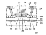
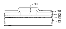
図3は、本発明の第1実施形態に係る低温ポリシリコンTFTの断面図である。図3に示すように、本発明の低温ポリシリコンTFT330は、主に基板300、キャップ層306、ポリシリコン薄膜308a、ゲート316及びソース/ドレイン導電層336からなる。このうち、キャップ層306は基板300上に配置され、本実施形態においては、基板における不純物が製造プロセス中に予期しない拡散を生じて素子の機能に影響することを防ぐよう、基板300上に、例えばキャップ層306と基板300との間にある緩衝層302を配置する。
FIG. 3 is a cross-sectional view of the low-temperature polysilicon TFT according to the first embodiment of the present invention. As shown in FIG. 3, the low-
特に、キャップ層306と緩衝層302との間に、更に隙間領域310を有する。隙間領域310内には、例えば熱伝導係数がより低い空気若しくはその他のガスがある。
In particular, a
ポリシリコン薄膜308aはキャップ層306上に配置され、チャネル領域322と不純物のドープされたソース/ドレイン領域318に分けられる。このうちチャネル領域322は隙間領域310の上に位置し、チャネル領域322内のポリシリコン薄膜308aが、低温ポリシリコンTFT330のポリシリコンチャネル層である。ゲート316はポリシリコン薄膜308aのチャネル領域322の上に配置され、ポリシリコン薄膜308a上に例えばゲート絶縁層314が配置される。
The polysilicon thin film 308a is disposed on the
誘電層324はゲート絶縁層314上に配置され、ゲート316を被覆する。また、誘電層324上にソース/ドレイン導電層336が配置され、ソース/ドレイン導電層336は、誘電層324とゲート絶縁層314との間に配置されるソース/ドレインコンタクトホール332を介してソース/ドレイン領域318と電気的に接続する。
A
注意すべきは、本実施形態において、チャネル領域322内のポリシリコン薄膜308a中にあるシリコン結晶粒340は、例えばソース/ドレイン領域318内のポリシリコン薄膜308a中にあるシリコン結晶粒350より大きく、好ましい大きさは、チャネル領域322の長さLの半分より大きい程度である。従って、低温ポリシリコンTFT330は、より高い駆動電流を有することができる。且つ、チャネル領域322内の結晶粒340の大きさがより大きいため、チャネル領域322内の結晶粒界360の数が、ソース/ドレイン領域318内の結晶粒界360の数より少ない。且つ、結晶粒の粒子配向が、電子の低温ポリシリコンTFT330内での伝送方向と平行であるので、低温ポリシリコンTFT330が作動状態であるとき、電子キャリアが容易にチャネル領域322を透過でき、チャネル領域322内の結晶粒界360が多すぎるため乱射され、電子移動度が低下することがない。
Note that in this embodiment, the
特に、本発明は低温ポリシリコンTFT330のゲート316の幅を縮小して、結晶粒340のサイズよりも小さくすることが可能であり(図4Aに示す)、よって薄膜トランジスタのチャネル領域が結晶粒界をまたぐのを防いで、薄膜トランジスタがより良い機能を持つことができる。この分野の通常の知識を有する者であれば分かるように、ここでいう結晶粒サイズとは、通常ゲートの幅と平行な方向上の結晶粒の長さを指す。
In particular, the present invention can reduce the width of the
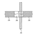
ゲートの幅を縮小する以外、本発明は、更に低温ポリシリコンTFT上に、本発明の別の実施形態に係る低温ポリシリコンTFTの平面図である図4Bに示すようなダブルゲート構造416を配置することができる。このようなダブルゲート構造416も、電子が直接チャネル中央の唯一の結晶粒界の影響を受けるのを減少して、トランジスタの機能を明らかに向上させることができる。
Other than reducing the gate width, the present invention further disposes a
本発明は、特殊な製造プロセスにより、上記チャネル領域が好ましい特性を有する低温ポリシリコンTFTを製造する。以下で実施形態を挙げて上記低温ポリシリコンTFTのチャネル層の製造方法について説明する。 The present invention manufactures a low-temperature polysilicon TFT in which the channel region has preferable characteristics by a special manufacturing process. A method for manufacturing the channel layer of the low-temperature polysilicon TFT will be described below with reference to an embodiment.
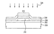
図5Aから図5Eは、本発明の第2実施形態に係る低温ポリシリコンTFTのチャネル層の製造フロー断面図である。また、図6Aから図6Cはそれぞれ図5Aから図5Cに対応する平面図であり、図6Dは図5Eに対応する平面図である。 FIG. 5A to FIG. 5E are cross-sectional views showing a manufacturing flow of the channel layer of the low-temperature polysilicon TFT according to the second embodiment of the present invention. 6A to 6C are plan views corresponding to FIGS. 5A to 5C, respectively, and FIG. 6D is a plan view corresponding to FIG. 5E.
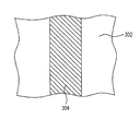
図5Aに示すように、まず基板300上に緩衝層302及び犠牲層304を順に、例えばCVD法若しくはスパッタ法により形成する。また、犠牲層304の材質は例えば金属材料である。更に注意すべきは、緩衝層302は選択性の層であって、その機能は前記の実施形態のとおりであるので、ここでは特に述べない。また、この分野の通常の知識を有する者が実際の製造プロセスの必要に応じて緩衝層302を設けても設けなくてもよく、本発明はこれを限定しない。また、犠牲層304は、例えば図6Aに示すような、緩衝層302上に配置された長方形パターンの膜層である。
As shown in FIG. 5A, first, a
図5B及び図6Bに示すように、緩衝層302上にキャップ層306及びアモルファスシリコン薄膜308を順に形成して、犠牲層304を被覆する。このうち、後続の製造プロセスにおいて犠牲層304上方の領域312内に低温ポリシリコンTFTのチャネル層を形成し、領域312の両側にソース/ドレイン領域を形成する。従って、犠牲層304の幅が該低温ポリシリコンTFTのチャネル層の長さを決定する。つまり、犠牲層304の幅を制御することにより、低温ポリシリコンTFTにおけるチャネル領域の長さを有効に制御できる。
As shown in FIGS. 5B and 6B, a
図5C及び図6Cに示すように、次に犠牲層304を除去して、キャップ層306と緩衝層302との間に、例えば空気が充填している隙間領域310を形成する。このステップは、ウェットエッチングにより犠牲層304を除去し、例えば図5Bに示すような構造をエッチング液に浸す(図示せず)。また、このエッチング液の犠牲層304に対するエッチング速度が他の膜層のエッチング速度よりはるかに大きいので、このステップにより他の膜層が完全に保持されたまま犠牲層304を除去することができる。
As shown in FIGS. 5C and 6C, the
図5D及び図5Eに示すように、隙間領域310を形成した後、続いてレーザアニール工程によりアモルファスシリコン薄膜308を溶融して再結晶させてポリシリコン薄膜308aを形成し、隙間領域310の上方にあるキャップ層306上にポリシリコンチャネル層522(つまり、領域312内に位置するポリシリコン薄膜308a)を形成する。本実施形態が使用するレーザアニール工程は、例えばエキシマレーザアニール工程であり、図5Dに示すように、エキシマレーザビーム326でアモルファスシリコン薄膜308を照射して溶融させ、液態シリコンとする(図示せず)。一定時間経過すると、液態シリコンが次第に冷えて再結晶し、ポリシリコン薄膜となる。この際、領域312が隙間領域310の上方に位置し、隙間領域310内には、例えば空気が存在しており、空気の熱伝導係数は0.025W/cm2Kであり、キャップ層306及び緩衝層302の熱伝導係数よりはるかに小さい。従って、領域312内の液態シリコンの結晶速度が両側の液態シリコンの結晶速度より遅くなる。つまり、結晶化の過程において、シリコン原子が両側から領域312の中央に向かって横方向に結晶粒を成長させてポリシリコン薄膜308aを形成する。図5E及び図6Dに示すように、この領域312内のポリシリコン薄膜308aがトランジスタのポリシリコンチャネル層522である。
As shown in FIG. 5D and FIG. A polysilicon channel layer 522 (that is, a polysilicon thin film 308 a located in the region 312) is formed on a
特に、領域312中にある結晶粒の成長速度が遅いため、形成された結晶粒のサイズも、両側領域内で形成された結晶粒より大きく、つまり、ポリシリコンチャネル層522中にある結晶粒のサイズがより大きく、例えばポリシリコンチャネル層522の長さLの半分よりやや大きい。
In particular, since the growth rate of the crystal grains in the
この他、ポリシリコンチャネル層522内の結晶粒界の数は、両側領域中にある結晶粒界の数より少ないので、電子がポリシリコンチャネル層522内においてより好ましい移動度を有し、トランジスタの電気特性を向上させる。
In addition, since the number of crystal grain boundaries in the
以上、本発明の実施例を図面を参照して詳述してきたが、具体的な構成は、この実施例に限られるものではなく、本発明の要旨を逸脱しない範囲の設計変更等があっても、本発明に含まれる。 The embodiment of the present invention has been described in detail with reference to the drawings. However, the specific configuration is not limited to this embodiment, and there are design changes and the like that do not depart from the gist of the present invention. Are also included in the present invention.
100、300 基板
102、308 アモルファスシリコン薄膜
102a、202a、308a ポリシリコン薄膜
104 マスク
106、326 エキシマレーザビーム
108 ホール
110、312 領域
302 緩衝層
304 犠牲層
306 キャップ層
310 隙間領域
314 ゲート絶縁層
316 ゲート
318 ソース/ドレイン領域
322 チャネル領域
324 誘電層
330 低温ポリシリコンTFT
332 ソース/ドレインコンタクトホール
336 ソース/ドレイン導電層
340、350 シリコン結晶粒
416 ダブルゲート構造
522 ポリシリコンチャネル層
100, 300 substrates
102, 308 Amorphous silicon thin film
102a, 202a, 308a Polysilicon thin film
104 mask
106, 326 Excimer laser beam
108 holes
110, 312 area
302 Buffer layer
304 Sacrificial layer
306 Cap layer
310 Clearance area
314 Gate insulation layer
316 gate
318 Source / drain region
322 channel region
324 Dielectric layer
330 Low temperature polysilicon TFT
332 source / drain contact holes
336 Source / drain conductive layer
340, 350 silicon crystal grains
416 Double gate structure
522 Polysilicon channel layer
Claims (13)
基板上方に配置され、基板との間に隙間領域があるキャップ層と、
前記キャップ層上に配置され、チャネル領域及び前記チャネル領域の両側に位置するソース/ドレイン領域を備え、前記チャネル領域が前記隙間領域の上にあるポリシリコン薄膜と、
前記ポリシリコン薄膜の前記チャネル領域上方に配置されたゲートと、
を備えることを特徴とする低温ポリシリコンTFT構造。 A low temperature polysilicon TFT structure suitable for placement on a substrate,
A cap layer disposed above the substrate and having a gap region between the substrate and
A polysilicon thin film disposed on the cap layer, comprising a channel region and source / drain regions located on both sides of the channel region, wherein the channel region is on the gap region;
A gate disposed above the channel region of the polysilicon thin film;
A low-temperature polysilicon TFT structure characterized by comprising:
前記誘電層上に配置され、前記誘電層における前記コンタクトホールと前記ポリシリコン薄膜の前記ソース/ドレイン領域により電気的接続をするソース/ドレイン導電層と、
を更に備えることを特徴とする請求項1に記載の低温ポリシリコンTFT構造。 A dielectric layer disposed on the polysilicon thin film and the gate, having a plurality of contact holes and exposing the source / drain regions of the polysilicon thin film;
A source / drain conductive layer disposed on the dielectric layer and electrically connected by the contact hole in the dielectric layer and the source / drain region of the polysilicon thin film;
The low-temperature polysilicon TFT structure according to claim 1, further comprising:
前記基板上にキャップ層を形成して前記犠牲層を被覆するステップと、
前記キャップ層上にアモルファスシリコン薄膜を形成するステップと、
前記犠牲層を除去して、前記基板と前記キャップ層との間に隙間領域を形成するステップと、
前記アモルファスシリコン薄膜を溶融させた後再結晶させて、前記隙間領域上方の前記キャップ層上にポリシリコンチャネル層を形成するステップと、
を含む低温ポリシリコンTFTのチャネル層の製造方法。 Forming a sacrificial layer on the substrate;
Forming a cap layer on the substrate to cover the sacrificial layer;
Forming an amorphous silicon thin film on the cap layer;
Removing the sacrificial layer to form a gap region between the substrate and the cap layer;
Remelting and then recrystallizing the amorphous silicon thin film to form a polysilicon channel layer on the cap layer above the gap region;
A method for manufacturing a channel layer of a low-temperature polysilicon TFT including:
11. The method of manufacturing a channel layer of a low-temperature polysilicon TFT according to claim 10, wherein the method of melting the amorphous silicon thin film includes excimer laser annealing.
Applications Claiming Priority (1)
| Application Number | Priority Date | Filing Date | Title |
|---|---|---|---|
| TW093109339A TWI228832B (en) | 2004-04-05 | 2004-04-05 | Structure of LTPS-TFT and fabricating method of channel layer thereof |
Publications (1)
| Publication Number | Publication Date |
|---|---|
| JP2005294851A true JP2005294851A (en) | 2005-10-20 |
Family
ID=35059713
Family Applications (1)
| Application Number | Title | Priority Date | Filing Date |
|---|---|---|---|
| JP2005108557A Pending JP2005294851A (en) | 2004-04-05 | 2005-04-05 | Low temperature polysilicon TFT structure and method of manufacturing channel layer thereof |
Country Status (3)
| Country | Link |
|---|---|
| US (2) | US20050224876A1 (en) |
| JP (1) | JP2005294851A (en) |
| TW (1) | TWI228832B (en) |
Cited By (2)
| Publication number | Priority date | Publication date | Assignee | Title |
|---|---|---|---|---|
| JP2016100537A (en) * | 2014-11-25 | 2016-05-30 | 株式会社ブイ・テクノロジー | Thin film transistor, thin film transistor manufacturing method and laser annealing device |
| KR20170124523A (en) * | 2016-04-01 | 2017-11-10 | 보에 테크놀로지 그룹 컴퍼니 리미티드 | Tft array substrate, method for manufacturing the same, and display device |
Families Citing this family (8)
| Publication number | Priority date | Publication date | Assignee | Title |
|---|---|---|---|---|
| US7381586B2 (en) | 2005-06-16 | 2008-06-03 | Industrial Technology Research Institute | Methods for manufacturing thin film transistors that include selectively forming an active channel layer from a solution |
| TWI295855B (en) * | 2006-03-03 | 2008-04-11 | Ind Tech Res Inst | Double gate thin-film transistor and method for forming the same |
| US7972943B2 (en) * | 2007-03-02 | 2011-07-05 | Semiconductor Energy Laboratory Co., Ltd. | Manufacturing method of semiconductor device |
| KR102368593B1 (en) * | 2015-04-03 | 2022-03-03 | 삼성디스플레이 주식회사 | Thin film transistor substrate and display panel having the same |
| CN105161498B (en) * | 2015-08-03 | 2017-09-19 | 京东方科技集团股份有限公司 | Thin film transistor (TFT) and preparation method thereof, array base palte and display device |
| CN105957805B (en) * | 2016-06-29 | 2018-12-18 | 京东方科技集团股份有限公司 | Making method for low-temperature multi-crystal silicon film, thin film transistor (TFT), array substrate and display device |
| US10355034B2 (en) * | 2017-08-21 | 2019-07-16 | Wuhan China Star Optoelectronics Technology Co., Ltd. | Low-temperature polycrystalline silicon array substrate and manufacturing method, display panel |
| JP7261567B2 (en) * | 2018-11-26 | 2023-04-20 | 株式会社Screenホールディングス | Substrate processing method and substrate processing apparatus |
Family Cites Families (4)
| Publication number | Priority date | Publication date | Assignee | Title |
|---|---|---|---|---|
| AU2001286432A1 (en) * | 2000-08-14 | 2002-02-25 | Matrix Semiconductor, Inc. | Dense arrays and charge storage devices, and methods for making same |
| US20030155572A1 (en) * | 2002-02-19 | 2003-08-21 | Min-Koo Han | Thin film transistor and method for manufacturing thereof |
| TWI231996B (en) * | 2003-03-28 | 2005-05-01 | Au Optronics Corp | Dual gate layout for thin film transistor |
| TW578310B (en) * | 2003-04-02 | 2004-03-01 | Au Optronics Corp | Low temperature poly silicon thin film transistor and method of forming poly silicon layer of the same |
-
2004
- 2004-04-05 TW TW093109339A patent/TWI228832B/en not_active IP Right Cessation
- 2004-07-30 US US10/710,729 patent/US20050224876A1/en not_active Abandoned
-
2005
- 2005-04-05 JP JP2005108557A patent/JP2005294851A/en active Pending
- 2005-09-15 US US11/162,569 patent/US20060008953A1/en not_active Abandoned
Cited By (8)
| Publication number | Priority date | Publication date | Assignee | Title |
|---|---|---|---|---|
| JP2016100537A (en) * | 2014-11-25 | 2016-05-30 | 株式会社ブイ・テクノロジー | Thin film transistor, thin film transistor manufacturing method and laser annealing device |
| WO2016084702A1 (en) * | 2014-11-25 | 2016-06-02 | 株式会社ブイ・テクノロジー | Thin-film transistor, method for manufacturing thin-film transistor, and laser annealing device |
| US10211343B2 (en) | 2014-11-25 | 2019-02-19 | V Technology Co., Ltd. | Thin film transistor, manufacturing process for thin film transistor, and laser annealing apparatus |
| US10535778B2 (en) | 2014-11-25 | 2020-01-14 | V Technology Co., Ltd. | Thin film transistor, manufacturing process for thin film transistor, and laser annealing apparatus |
| US10622484B2 (en) | 2014-11-25 | 2020-04-14 | V Technology Co., Ltd. | Thin film transistor, manufacturing process for thin film transistor, and laser annealing apparatus |
| KR20170124523A (en) * | 2016-04-01 | 2017-11-10 | 보에 테크놀로지 그룹 컴퍼니 리미티드 | Tft array substrate, method for manufacturing the same, and display device |
| US10325938B2 (en) | 2016-04-01 | 2019-06-18 | Boe Technology Group Co., Ltd. | TFT array substrate, method for manufacturing the same, and display device |
| KR102055247B1 (en) * | 2016-04-01 | 2019-12-11 | 보에 테크놀로지 그룹 컴퍼니 리미티드 | Tft array substrate, method for manufacturing the same, and display device |
Also Published As
| Publication number | Publication date |
|---|---|
| TW200534484A (en) | 2005-10-16 |
| US20050224876A1 (en) | 2005-10-13 |
| US20060008953A1 (en) | 2006-01-12 |
| TWI228832B (en) | 2005-03-01 |
Similar Documents
| Publication | Publication Date | Title |
|---|---|---|
| US6410373B1 (en) | Method of forming polysilicon thin film transistor structure | |
| KR100785020B1 (en) | Bottom gate thin film transistor and method of manufacturing same | |
| JP2005303299A (en) | Electronic device and manufacturing method thereof | |
| KR20030069779A (en) | Thin film transistor and method for manufacturing thereof | |
| JP2005294851A (en) | Low temperature polysilicon TFT structure and method of manufacturing channel layer thereof | |
| TWI520219B (en) | Method of forming polycrystalline germanium layer and method of manufacturing thin film transistor | |
| JP6081689B2 (en) | Polycrystalline silicon layer, thin film transistor, and organic electroluminescent display device manufacturing method | |
| JPH02275641A (en) | Manufacture of semiconductor device | |
| JP4549842B2 (en) | Thin film transistor manufacturing method | |
| US6387779B1 (en) | Method of crystallizing a silicon film and thin film transistor and fabricating method thereof using the same | |
| US7435667B2 (en) | Method of controlling polysilicon crystallization | |
| KR100915073B1 (en) | Method for crystallizing semiconductor film and semiconductor film crystallized by the method | |
| JPH1084114A (en) | Thin film semiconductor device and method of manufacturing the same | |
| KR19980083097A (en) | Crystallization method of amorphous silicon layer and manufacturing method of thin film transistor using same | |
| JP2007184562A (en) | Method for producing polycrystalline silicon film and method for producing thin film transistor using the same | |
| CN100391009C (en) | Low-temperature polycrystalline silicon thin film transistor and manufacturing method of channel layer thereof | |
| JP2004063478A (en) | Thin film transistor and method of manufacturing the same | |
| US7115449B2 (en) | Method for fabrication of polycrystalline silicon thin film transistors | |
| CN100570836C (en) | Polycrystalline silicon thin film transistor and manufacturing method thereof | |
| WO2006007757A1 (en) | A low temperature poly-silicon thin film transistor | |
| JP2008198643A (en) | Crystalline semiconductor film manufacturing method and active matrix substrate manufacturing method | |
| CN114242735B (en) | Array substrate, manufacturing method and mobile terminal | |
| CN100413040C (en) | Formation method of polysilicon thin film transistor | |
| CN2717022Y (en) | Low Temperature Polysilicon Thin Film Transistor | |
| US20060172469A1 (en) | Method of fabricating a polycrystalline silicon thin film transistor |
Legal Events
| Date | Code | Title | Description |
|---|---|---|---|
| A977 | Report on retrieval |
Free format text: JAPANESE INTERMEDIATE CODE: A971007 Effective date: 20070724 |
|
| A131 | Notification of reasons for refusal |
Free format text: JAPANESE INTERMEDIATE CODE: A131 Effective date: 20070801 |
|
| A02 | Decision of refusal |
Free format text: JAPANESE INTERMEDIATE CODE: A02 Effective date: 20071226 |