JP2005294831A - Heterojunction bipolar transistor - Google Patents
Heterojunction bipolar transistor Download PDFInfo
- Publication number
- JP2005294831A JP2005294831A JP2005091373A JP2005091373A JP2005294831A JP 2005294831 A JP2005294831 A JP 2005294831A JP 2005091373 A JP2005091373 A JP 2005091373A JP 2005091373 A JP2005091373 A JP 2005091373A JP 2005294831 A JP2005294831 A JP 2005294831A
- Authority
- JP
- Japan
- Prior art keywords
- suppression layer
- base
- collector
- tunneling
- hbt
- Prior art date
- Legal status (The legal status is an assumption and is not a legal conclusion. Google has not performed a legal analysis and makes no representation as to the accuracy of the status listed.)
- Pending
Links
Images
Classifications
-
- H—ELECTRICITY
- H10—SEMICONDUCTOR DEVICES; ELECTRIC SOLID-STATE DEVICES NOT OTHERWISE PROVIDED FOR
- H10D—INORGANIC ELECTRIC SEMICONDUCTOR DEVICES
- H10D10/00—Bipolar junction transistors [BJT]
- H10D10/80—Heterojunction BJTs
- H10D10/821—Vertical heterojunction BJTs
-
- H—ELECTRICITY
- H10—SEMICONDUCTOR DEVICES; ELECTRIC SOLID-STATE DEVICES NOT OTHERWISE PROVIDED FOR
- H10D—INORGANIC ELECTRIC SEMICONDUCTOR DEVICES
- H10D10/00—Bipolar junction transistors [BJT]
- H10D10/01—Manufacture or treatment
- H10D10/021—Manufacture or treatment of heterojunction BJTs [HBT]
-
- H—ELECTRICITY
- H10—SEMICONDUCTOR DEVICES; ELECTRIC SOLID-STATE DEVICES NOT OTHERWISE PROVIDED FOR
- H10D—INORGANIC ELECTRIC SEMICONDUCTOR DEVICES
- H10D62/00—Semiconductor bodies, or regions thereof, of devices having potential barriers
- H10D62/10—Shapes, relative sizes or dispositions of the regions of the semiconductor bodies; Shapes of the semiconductor bodies
- H10D62/13—Semiconductor regions connected to electrodes carrying current to be rectified, amplified or switched, e.g. source or drain regions
- H10D62/137—Collector regions of BJTs
-
- H—ELECTRICITY
- H10—SEMICONDUCTOR DEVICES; ELECTRIC SOLID-STATE DEVICES NOT OTHERWISE PROVIDED FOR
- H10D—INORGANIC ELECTRIC SEMICONDUCTOR DEVICES
- H10D62/00—Semiconductor bodies, or regions thereof, of devices having potential barriers
- H10D62/80—Semiconductor bodies, or regions thereof, of devices having potential barriers characterised by the materials
- H10D62/82—Heterojunctions
- H10D62/824—Heterojunctions comprising only Group III-V materials heterojunctions, e.g. GaN/AlGaN heterojunctions
-
- H—ELECTRICITY
- H10—SEMICONDUCTOR DEVICES; ELECTRIC SOLID-STATE DEVICES NOT OTHERWISE PROVIDED FOR
- H10D—INORGANIC ELECTRIC SEMICONDUCTOR DEVICES
- H10D62/00—Semiconductor bodies, or regions thereof, of devices having potential barriers
- H10D62/80—Semiconductor bodies, or regions thereof, of devices having potential barriers characterised by the materials
- H10D62/85—Semiconductor bodies, or regions thereof, of devices having potential barriers characterised by the materials being Group III-V materials, e.g. GaAs
- H10D62/852—Semiconductor bodies, or regions thereof, of devices having potential barriers characterised by the materials being Group III-V materials, e.g. GaAs being Group III-V materials comprising three or more elements, e.g. AlGaN or InAsSbP
Landscapes
- Bipolar Transistors (AREA)
Abstract
Description
本発明は、ヘテロ接合バイポーラ・トランジスタ(HBT)に関する。 The present invention relates to heterojunction bipolar transistors (HBTs).
インジウム燐ヘテロ接合バイポーラ・トランジスタ(InP-HBT)は、高周波数動作、及び、10〜20ボルトといった比較的高い降伏電圧(breakdown voltage)が望ましい用途において有用である。近似関係式fMAX=√(fT/8πRbCc)(ここで、fTは電流・利得・帯域幅の積、すなわち、カットオフ周波数であり、Rbはベース直列抵抗であり、Ccは、コレクタ・ベース・キャパシタンスである)は、fTが増すと、最大動作周波数fMAXが増すことを示している。この関係式は、トランジスタの単純な集中素子(lumped-element)モデルに基づいているため、おおよそのものである。実際には、ベース直列抵抗Rb及びコレクタ・ベース・キャパシタンスCcは、分散している。より正確な式は、代数的に複雑であり、この近似式を用いて、立証しようとする点を明らかにするよりも、不明瞭にすることになる。 Indium-phosphorus heterojunction bipolar transistors (InP-HBT) are useful in applications where high frequency operation and relatively high breakdown voltages such as 10-20 volts are desired. Approximate relational expression f MAX = √ (f T / 8πR b C c ) (where f T is a product of current, gain and bandwidth, that is, a cutoff frequency, R b is a base series resistance, and C (c is the collector-base capacitance) indicates that the maximum operating frequency f MAX increases as f T increases. This relation is approximate because it is based on a simple lumped-element model of the transistor. In practice, the base series resistance Rb and the collector base capacitance Cc are distributed. More accurate formulas are algebraically complex and will be obscured rather than using this approximation to reveal the point to be verified.
p−n接合の降伏電圧は、逆電圧であり、それを超えると、電圧のわずかな上昇によって、大電流を生じることになる。バイポーラ・トランジスタにおける降伏電圧の定義が2つある。電圧BVCEOは、ベース端末を開放して測定されたトランジスタ降伏電圧である。電圧BVCBOは、エミッタ端子を開放して測定されたベース・コレクタ接合の降伏電圧である。ベース材料として砒化アンチモン化ガリウム(GaAsSb)を含むインジウム燐(InP)HBTの場合、BVCBOは、HBTのベースの価電子帯からコレクタの伝導帯への電子の「ツェナー」・トンネリング(Zener tunneling)と呼ばれる現象によって制限される。これによって生じる電流は、「トンネル電流(tunneling current)」と呼ばれる。一般に、トンネル電流が流れる電圧を最大にするのが望ましい。 The breakdown voltage of the pn junction is a reverse voltage, and beyond this, a slight increase in voltage will cause a large current. There are two definitions of breakdown voltage in bipolar transistors. The voltage BV CEO is the transistor breakdown voltage measured with the base terminal open. The voltage BV CBO is the breakdown voltage of the base-collector junction measured with the emitter terminal open. In the case of indium phosphide (InP) HBTs with gallium arsenide arsenide (GaAsSb) as the base material, BV CBO is the “Zener tunneling” of electrons from the valence band of the base of the HBT to the conduction band of the collector. Limited by a phenomenon called The resulting current is called “tunneling current”. In general, it is desirable to maximize the voltage through which the tunnel current flows.
GaAsSb/InP HBTは、優れた高周波(高fT及びfMAX)性能を示す。GaAsSbベースは、InPコレクタと共に「タイプII」バンド・ラインアップ(type-II band lineup)と称するものを形成する。伝導帯(conduction band)のオフセットによって、ベースからコレクタへの電子伝達が向上し、価電子帯(valence band)のオフセットによって、ベースからコレクタへの正孔の伝達が最小限に抑えられるので、バンド・ラインアップは、多くの点で理想的である。タイプIIバンド・ラインアップによって、HBTの所望の「ニー」・ターンオン特性(knee turn-on characteristic)が得られるようになる。良好なニー・ターンオン特性は、比較的低いコレクタ電圧での動作を可能し、HBTが組み込まれることになる多くの回路の効率の良い動作にとって重要である。 GaAsSb / InP HBT shows excellent high-frequency (high f T and f MAX) performance. The GaAsSb base forms what is referred to as a “type-II” band lineup with an InP collector. The conduction band offset improves the electron transfer from the base to the collector, and the valence band offset minimizes hole transfer from the base to the collector.・ The lineup is ideal in many ways. The Type II band lineup provides the desired “knee” turn-on characteristic of the HBT. Good knee turn-on characteristics are important for the efficient operation of many circuits that allow operation at relatively low collector voltages and that will incorporate an HBT.
GaAsSb/InP HBTは、上述の利点を備えているが、いくつかの潜在的な用途には降伏電圧が不十分である。本発明の目的は、上述の利点を備えるが、降伏電圧を増大させる、GaAsSb/InP HBTを提供することにある。 While GaAsSb / InP HBT has the advantages described above, the breakdown voltage is insufficient for some potential applications. An object of the present invention is to provide a GaAsSb / InP HBT having the above-mentioned advantages but increasing the breakdown voltage.
本発明によれば、基板上に形成されたコレクタと、コレクタ上に形成されたベースと、ベース上に形成されたエミッタと、コレクタとベースの間のトンネリング抑制層を含む、ヘテロ接合バイポーラ・トランジスタ(HBT)が得られる。トンネリング抑制層は、ベース材料とは異なり、ベース材料の電子親和力以上の電子親和力(electron affinity)を備える材料から製作される。 In accordance with the present invention, a heterojunction bipolar transistor comprising a collector formed on a substrate, a base formed on the collector, an emitter formed on the base, and a tunneling suppression layer between the collector and base. (HBT) is obtained. Unlike the base material, the tunneling suppression layer is made of a material having an electron affinity that is equal to or higher than the electron affinity of the base material.
本発明によれば、さらに、基板を設けるステップと、基板上にサブコレクタを形成するステップと、サブコレクタの上にコレクタを形成するステップと、コレクタの上にトンネリング抑制層を形成するステップと、トンネリング抑制層の上にベースを形成するステップと、ベースの上にエミッタを形成するステップが含まれている、HBTを製作するための方法も得られる。 According to the present invention, further, a step of providing a substrate, a step of forming a subcollector on the substrate, a step of forming a collector on the subcollector, and a step of forming a tunneling suppression layer on the collector; A method for fabricating an HBT is also provided that includes forming a base on the tunneling suppression layer and forming an emitter on the base.
トンネリング抑制層は、ベースの価電子帯からコレクタの伝導帯への電子のトンネリングの確率を低下させることによって、HBTの降伏電圧を高める。 The tunneling suppression layer increases the breakdown voltage of the HBT by reducing the probability of electron tunneling from the base valence band to the collector conduction band.
本発明は、付属の図面を参照することによってより明確に理解することが可能になる。図面の構成要素は、必ずしも一定の拡大率によるものではなく、代わりに、本発明の原理を明瞭に例証することに重点がおかれている。さらに、図面中、同様の参照番号は、いくつかの図にわたって対応する部分を表わしている。 The invention can be more clearly understood with reference to the accompanying drawings. The components in the drawings are not necessarily to scale, emphasis instead being placed upon clearly illustrating the principles of the present invention. Moreover, in the drawings, like reference numerals designate corresponding parts throughout the several views.
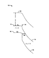
図1には、GaAsSbベースとInPコレクタを備えたHBTのベース・コレクタ接合のバンドダイアグラム(band diagram)10が示されており、タイプIIバンド・ラインアップが示されている。バンドダイアグラム10には、デバイスの層面に対して直交する方向への物理的距離に対する電子エネルギがプロットされている。バンドダイアグラム10には、伝導帯エネルギEc(ベースに関する12及びコレクタに関する14)、価電子帯エネルギEv(ベースに関する16及びコレクタに関する18)、及び、逆バイアス下における真空レベル22が示されている。真空レベルは、自由電子のエネルギを定義する基準である。電子親和力χは、半導体の真空レベル22と伝導帯エネルギEcとのエネルギ差である。電子親和力χは、半導体の伝導体に存在する電子を解放するのに必要なエネルギである。真空レベルは連続的であるため、伝導帯オフセットは、2つの半導体間における電子親和力の差である。
FIG. 1 shows a band diagram 10 of a base-collector junction of an HBT with a GaAsSb base and an InP collector, showing a type II band lineup. The band diagram 10 plots the electron energy against the physical distance in a direction perpendicular to the layer plane of the device. Band diagram 10 shows conduction band energy Ec (12 for base and 14 for collector), valence band energy Ev (16 for base and 18 for collector), and
GaAsSb/InP HBTのバンド・ラインアップは、電子伝達を促進するが、ベースの価電子帯からコレクタの伝導帯への電子のトンネリングの確率を増すので、好ましくない。トンネリングの確率は、ベースの価電子帯とコレクタの伝導帯との距離が、図1に矢印26で示すように、比較的短いために高くなる。トンネリングの確率が高くなると、降伏電圧BVCBOが低下する。トンネリング距離以外に、トンネリングの確率は、ベース・コレクタ接合におけるエネルギ障壁、エネルギ障壁における電子及び正孔の質量、及び、トンネリングに利用可能な状態の密度といった、いくつかの要因にも左右される。
The band lineup of GaAsSb / InP HBTs facilitates electron transfer but is not preferred because it increases the probability of electron tunneling from the base valence band to the collector conduction band. The probability of tunneling is high because the distance between the base valence band and the collector conduction band is relatively short, as shown by the
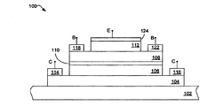
図2は、本発明の実施態様の1つに従って構成されたヘテロ接合バイポーラ・トランジスタ(HBT)100を例示したブロック図である。HBT100は、さまざまな半導体材料系を利用して形成することが可能である。この例の場合、HBTの半導体層は、インジウム燐(InP)基板102上に形成される。厚さ約500ナノメートル(nm)のインジウム燐層が、インジウム燐層102の上に成長させられて、サブコレクタ104を形成する。厚さ約300ナノメートル(nm)のインジウム燐層が、サブコレクタ104の上に成長させられて、コレクタ106を形成する。
FIG. 2 is a block diagram illustrating a heterojunction bipolar transistor (HBT) 100 configured in accordance with one embodiment of the present invention. The HBT 100 can be formed using various semiconductor material systems. In this example, the HBT semiconductor layer is formed on an indium phosphide (InP)
トンネリング抑制層110が、コレクタ106の上に成長させられる。トンネリング抑制層110は、アルミニウム、ガリウム、インジウム、窒素、燐、砒素、及び、アンチモンのうち2つ以上の元素を含む材料から製作される。例えば、トンネリング抑制層110は、砒化アルミニウム・ガリウム・インジウム(AlGaInAs)または砒化燐化アルミニウム・インジウム(AlInAsP)を利用して製作することが可能である。実施態様の1つでは、トンネリング抑制層110は、Al0.33Ga0.15In0.52Asの組成を有するAlGaInAsを利用して製作される。HBT100の所望の特性に従って、他の組成を利用することも可能である。例えば、AlGaInAsの組成は、Al1-x-yGaxInyAsとすることも可能である。ここで、0.09≦x≦0.25、及び、y=0.52。トンネリング抑制層110は、約10〜50nmの厚さまで成長させられるが、一般には、約25nmの厚さである。
A
厚さ約30nmの砒化アンチモン化ガリウム(GaAsSb)の層が、トンネリング抑制層110の上に成長させられて、ベース108を形成する。厚さ約100nmのインジウム燐の層が、ベース108の上に形成されて、エミッタ112を形成する。エミッタは、砒化アルミニウム・インジウム(AlInAs)、砒化アルミニウム・ガリウム・インジウム(AlGaInAs)、砒化燐化アルミニウム・インジウム(AlInAsP)、または、アルミニウム、ガリウム、インジウム、窒素、燐、砒素、及び、アンチモンのうち2つ以上の元素を含む別の組成といった、他の材料から形成することも可能である。次に、コレクタ接点114及び116、ベース接点118及び122、及び、エミッタ接点124が、それぞれ、サブコレクタ104、ベース108、及び、エミッタ112のそれぞれに達するエッチングの後、それらそれぞれの層の上に形成される。
A layer of gallium arsenide arsenide (GaAsSb) about 30 nm thick is grown on the
トンネリング抑制層110が、ベース108を形成する材料とは異なる材料から形成される。さらに、後述するように、トンネリング抑制層110を形成する材料の電子親和力χは、ベース108を形成する材料とは異なる材料の電子親和力以上である。トンネリング抑制層110を形成する材料とベース108を形成する材料の電子親和力の差は、例えば、およそ0.03eVほどになる可能性があるが、やはり、等しいとみなすことが可能である。この例の場合、トンネリング抑制層110の材料である砒化アルミニウム・ガリウム・インジウム(AlGaInAs)の組成は、ベース108の材料である砒化アンチモン化ガリウム(GaAsSb)の電子親和力以上の電子親和力χを備えるように選択される。
The
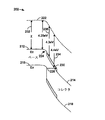
図3は、逆バイアス下における図2のトンネリング抑制層を含む、砒化アンチモン化ガリウム/インジウム燐(GaAsSb/InP)HBTのベース・コレクタ接合のバンドダイアグラムである。上述のように、バンドダイアグラム200には、距離に対する電子エネルギがプロットされている。真空レベルは、222で表示され、ベースにおける伝導帯のエネルギ準位は、参照番号212で表示され、コレクタにおける伝導帯のエネルギ準位は、参照番号214で表示されている。ベースにおける価電子帯のエネルギ準位は、参照番号216で表示され、コレクタにおける価電子帯のエネルギ準位は、参照番号218で表示されている。電子親和力χは、参照番号232で表示されている。GaAsSbベースにおける電子の電子親和力χは、約4.25eVである。
FIG. 3 is a band diagram of a base-collector junction of anti-gallium arsenide / indium phosphide (GaAsSb / InP) HBT including the tunneling suppression layer of FIG. 2 under reverse bias. As described above, the band diagram 200 plots electron energy against distance. The vacuum level is indicated by 222, the conduction band energy level at the base is indicated by
本発明の実施態様の1つによれば、図2に示すHBT100のコレクタ106とベース108との間にトンネリング抑制層110を配置することによって、電子が、トンネル効果でベースの価電子帯からコレクタの伝導帯まで移動しなければならない距離が長くなる。この距離が、矢印226によって示されており、トンネリング抑制層がないHBTと比較した場合の、電子が移動しなければならないトンネリング距離の延長を表わしている。点線230は、トンネリング抑制層110の伝導帯エネルギを示している。参考のため、点線230は、トンネリング抑制層のない場合の、コレクタの伝導帯エネルギ214の上に重ねて示されている。トンネリング抑制層の電子親和力χは、この例では約4.3eVである、矢印236で示されている。参考のため、InPコレクタの伝導帯における電子の電子親和力χは、4.4eVの電子親和力を表わす矢印234を利用して示されている。
According to one embodiment of the present invention, by arranging the
トンネリング抑制層110は、電子がトンネル効果でベースの価電子帯からコレクタの伝導帯に移動する確率を低下させることによって、HBT100の逆(降伏)電圧を上昇させる。電子がトンネル効果でベースの価電子帯からコレクタの伝導帯まで移動しなければならない距離は、事実上、矢印226で示すように長くなる。トンネリング抑制層110の電子親和力は、ベースの電子親和力にほぼ等しいか、それを超えるので、トンネリング抑制層110によって、ベースからコレクタへの所望の伝導体の流れが妨げられることはない。従って、HBT100の所望の「ニー(knee)」・ターンオン特性が維持され、HBT100は、低電圧において多量の電流の流れを示す。
The
ベースとトンネリング抑制層の110の接合224における電子親和力χがわずかにオフセットすると、伝導帯を介したベースからコレクタへの電子の移動に対する障壁が弱まる(すなわち、エネルギが増大する)ことになる。
If the electron affinity χ at the
トンネル抑制層110を導入する効果の相殺は、トンネリング抑制層110に一般的に利用可能な組成(砒化アルミニウム・ガリウム・インジウムまたは砒化燐化アルミニウム・インジウム)の大部分が、インジウム燐に比べて、トンネル効果で移動する電子の有効質量が小さいこと、及び、正孔トンネリング障壁が小さいこと(価電子帯のオフセット)の一方または両方によって生じる。これら両方の効果が、トンネリングの確率を高め、従って、降伏電圧を低下させる働きをする。これらの効果は、トンネリング抑制層110によって生じるトンネリング距離の延長とのトレードオフを生じる。トンネリング層110の設計を助け、トンネリング確率の低下を確認するため、シミュレーション研究が実施された。シミュレーション結果から明らかなように、トンネリング抑制層110は、コレクタ電流を減少させ、従って、ある特定のコレクタ・ベース電圧に関して、HBTにおけるトンネリング確率を低下させることになる。
The effect of introducing the
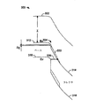
図4は、逆バイアス化における図2のトンネリング抑制層の代替実施態様を含む、砒化アンチモン化ガリウム/インジウム燐(GaAsSb/InP)HBTのベース・コレクタ接合のバンドダイアグラム300である。図4のトンネリング抑制層は、傾斜(graded)電子親和力χを備えている。点線330は、電子がトンネリング抑制層に入り込むまでの距離に応じて変動する、傾斜電子親和力χを備えるトンネリング抑制層110を例示している。図5Bにおいて、ベースからトンネリング抑制層110への電子親和力のステップ324が、Δχによって表わされ、トンネリング抑制層110における電子親和力の増大は、Δχtによって表わされている。ベースとトンネリング抑制層110の接合324の近くにおける電子親和力χは、伝導帯を介してベースからコレクタへ移動する電子に対する障壁を弱めるため、わずかにオフセットしている。層の深さにわたる砒化アルミニウム・ガリウム・インジウム(AlGaInAs)のトンネリング抑制層の組成を変更することによって、所望の低ニー電圧をもたらし、さらに、トンネル電流を減少させる傾斜トンネリング抑制層が形成される。
FIG. 4 is a band diagram 300 of an anti-gallium arsenide / indium phosphide (GaAsSb / InP) HBT base-collector junction, including an alternative embodiment of the tunneling suppression layer of FIG. 2 in reverse biasing. The tunneling suppression layer of FIG. 4 has a graded electron affinity χ. A dotted
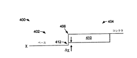
図5Aは、図3に示す、定電子親和力χを有するトンネリング抑制層の電子親和力を例示した概略図400である。ベース402とトンネリング抑制層410との接合412におけるトンネリング抑制層410の電子親和力χは、伝導帯を介して、ベースからコレクタに移動する電子に対する障壁を弱めるため、わずかにΔχだけオフセットしている。トンネリング抑制層410の電子親和力は、コレクタ404に向かって一定の状態を保つ。この例の場合、ほぼAl0.33Ga0.15In0.52Asの組成によって、約0.07eVのΔχが得られる。あるいはまた、GaAsSbベースと同じ電子親和力χを備える、ほぼAl0.37Ga0.11In0.52Asまでの組成は、伝導帯を介して、ベースからコレクタに移動する電子に対する障壁を強めるという代償を払って、利用することが可能である。
FIG. 5A is a schematic diagram 400 illustrating the electron affinity of the tunneling suppression layer having constant electron affinity χ shown in FIG. The electron affinity χ of the
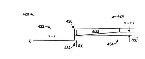
図5Bは、トンネリング抑制層110の深さに応じて変化する、電子親和力χを備えたトンネリング抑制層の電子親和力を例示した概略図420である。電子親和力の変化は、Al1-x-yGaxInyAs(ここで、0.09≦x≦0.25、及び、y=0.25)を含むトンネリング抑制層430を利用し、ベースの近くよりも、コレクタの近くのガリウムのモル分率を大きくすることによって実現することが可能である。例えば、xがトンネリング抑制層のベース側における約0.12からトンネリング抑制層のコレクタ側における約0.15に変化すると、ベース422の近くの領域432において約0.03eVのΔχと約0.04eVのΔχtが生じることになる。この例の場合、ベース422の近くの領域432における約0.03eVのΔχによって、伝導帯を介して、ベースからコレクタに移動する電子に対する障壁が弱まり、その傾斜によって、トンネリング抑制層430を横断する間に、これらの電子に余剰エネルギが付与される。トンネリング抑制層430の傾斜は、図4のバンドダイアグラムにおける点線330に対応する。
FIG. 5B is a schematic diagram 420 illustrating the electron affinity of a tunneling suppression layer with an electron affinity χ that varies with the depth of the
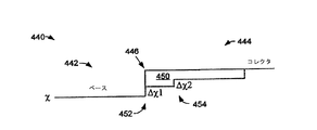
図5Cは、階段状傾斜電子親和力を備えたトンネリング抑制層を例示した概略図440である。ベース442の近くの遷移452におけるトンネリング抑制層450の電子親和力は、ベースの電子親和力よりもΔχ1だけ強く、遷移454まで一定のままであり、遷移454において、さらに、Δχ2の値だけ増大する。例えば、Al0.32Ga0.16In0.52Asの厚さ15nmの層が後続するAl0.35Ga0.13In0.52Asの厚さ10nmの層から構成されるトンネリング抑制層によって、図5Cに示す階段状傾斜構造が得られることになる。あるいはまた、InPとほぼ同じ電子親和力を備えることになるAl0.26Ga0.22In0.52Asまでの組成を利用することも可能である。さらに、トンネリング抑制層は、電子親和力がベースからコレクタまでの間に増大することになる、3つ以上の遷移を利用して形成することも可能になる。AlGaInAsの組成は、Al1-x-yGaxInyAsとすることが可能であり、ここで、0.09≦x≦0.25、及び、y=0.52である。
FIG. 5C is a schematic diagram 440 illustrating a tunneling suppression layer with stepped gradient electron affinity. The electron affinity of the
あるいはまた、トンネリング抑制層は、例えば、AlInAsとInPを組み合わせて形成されるAlInAsPの組成を利用して製作することも可能である。伝導帯においてGaAsSbと同じ電子親和力χを備える組成のAlInAsPは、41%のInPと50%のAlInAsを組み合わせることによって形成可能である。70%のInPと30%のAlInAsを組み合わせることによって、デルタχ=0.07eVの電子親和力のステップを導入することが可能である。この例は、Al0.48In0.52Asの組成を利用して生じる、InPに対して格子整合するように成長させたAlInAsに関するものである。伝導帯において、電子親和力χがGaAsSbの電子親和力を超えるAlInAsPの場合、100%InPの組成まで、利用するInP分率を高くすることが可能である。例えば、図5Bに示す傾斜を有するトンネリング抑制層は、ベースの近くにおいて58%のInPと42%のInAlAsを有し、コレクタの近くにおいて75%のInPと25%のInAlAsを有するInAlAsPの組成を利用し、その間を直線補間することによって形成可能である。この結果、Δχ=0.04eV及びΔχt=0.04eVになる。 Alternatively, the tunneling suppression layer can be manufactured using, for example, a composition of AlInAsP formed by combining AlInAs and InP. AlInAsP having a composition having the same electron affinity χ as GaAsSb in the conduction band can be formed by combining 41% InP and 50% AlInAs. By combining 70% InP and 30% AlInAs, it is possible to introduce an electron affinity step of delta χ = 0.07 eV. This example relates to AlInAs grown to lattice match with InP, which is generated using the composition of Al 0.48 In 0.52 As. In the case of AlInAsP in which the electron affinity χ exceeds the electron affinity of GaAsSb in the conduction band, it is possible to increase the InP fraction used up to a composition of 100% InP. For example, the sloped tunneling suppression layer shown in FIG. 5B has a composition of InAlAsP with 58% InP and 42% InAlAs near the base and 75% InP and 25% InAlAs near the collector. It can be formed by linear interpolation between them. As a result, Δχ = 0.04 eV and Δχ t = 0.04 eV.
代替実施態様の場合、トンネリング抑制層は、「ディジタル合金(alloy)」と呼ばれる合成物から形成することが可能である。AlGaInAsのトンネリング抑制層は、例えば、GaInAsの薄層と交互になったAlInAsの薄層を形成することによって、ディジタル合金から形成することが可能である。これらの層は、ある厚さの少数の層を利用して形成することが可能である。例えば、Al0.33Ga0.15In0.52Asのトンネリング抑制層は、Al0.48In0.52AsとGa0.47In0.53Asの交互層を利用して形成することが可能である。トンネリング抑制層の所望の特性に応じて、砒化アルミニウム・インジウム(AlInAs)とインジウム燐(InP)の交互層を含む砒化燐化アルミニウム・インジウム(AlInAsP)のような代替組成を形成することも可能である。 In an alternative embodiment, the tunneling suppression layer can be formed from a composite called a “digital alloy”. The AlGaInAs tunneling suppression layer can be formed from a digital alloy, for example, by forming thin AlInAs layers alternating with thin GaInAs layers. These layers can be formed using a small number of layers of a certain thickness. For example, a tunneling suppression layer of Al 0.33 Ga 0.15 In 0.52 As can be formed using alternating layers of Al 0.48 In 0.52 As and Ga 0.47 In 0.53 As. Depending on the desired properties of the tunneling suppression layer, alternative compositions such as aluminum indium arsenide arsenide (AlInAsP) including alternating layers of aluminum arsenide indium (AlInAs) and indium phosphide (InP) can be formed. is there.
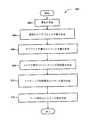
図6は、本発明の実施態様の1つに従ってHBTを製作する方法を明らかにしたフローチャートである。ブロック502では、インジウム燐の基板が設けられる。ブロック504では、インジウム燐のサブコレクタ層が形成される。ブロック506では、インジウム燐のコレクタ層が形成される。ブロック508では、トンネリング抑制層が形成される。トンネリング抑制層は、砒化アルミニウム・ガリウム・インジウム、砒化燐化アルミニウム・インジウム(AlInAsP)、または、アルミニウム、ガリウム、インジウム、窒素、燐、砒素、及び、アンチモンのうちの2つ以上の組み合わせを利用して、形成することが可能である。ブロック510では、アンチモン化ガリウム・砒素のベース層が形成される。ブロック512では、インジウム燐のエミッタ層が形成される。エミッタには、アルミニウム、ガリウム、窒素、砒素、及び、アンチモンのうち2つ以上を含むことも可能である。
FIG. 6 is a flowchart illustrating a method for fabricating an HBT according to one embodiment of the present invention. In
本開示では、例示の実施態様を利用して、本発明が詳述されている。しかし、云うまでもないが、付属の請求項によって定義される本発明は、上述の実施態様に厳密に制限されるものではない。 This disclosure describes the invention in detail using exemplary embodiments. However, it goes without saying that the invention defined by the appended claims is not strictly limited to the embodiments described above.
100 ヘテロ接合バイポーラ・トランジスタ
102 基板
106 コレクタ
108 ベース
110 トンネリング抑制層
112 エミッタ
100 heterojunction
Claims (10)
前記コレクタの上に形成されるベースと、
前記ベースの上に形成されるエミッタと、
前記ベースの材料と異なり、前記ベースの材料の電子親和力以上の電子親和力を備える材料から製作された、前記コレクタと前記ベースの間に位置するトンネリング抑制層と、
を有する、ヘテロ接合バイポーラ・トランジスタ(HBT)。 A collector formed on a substrate;
A base formed on the collector;
An emitter formed on the base;
Unlike the base material, a tunneling suppression layer located between the collector and the base made of a material having an electron affinity greater than or equal to the electron affinity of the base material;
A heterojunction bipolar transistor (HBT).
前記トンネリング抑制層は、前記ベース付近よりも前記コレクタ付近でガリウムのモル分率が大きい、
請求項6に記載のヘテロ接合バイポーラ・トランジスタ(HBT)。 The tunneling suppression layer consists essentially of Al 1-xy Ga x In y As, where 0.09 ≦ x ≦ 0.25 and y = 0.52;
The tunneling suppression layer has a greater molar fraction of gallium near the collector than near the base;
The heterojunction bipolar transistor (HBT) according to claim 6.
基板を設けるステップと、
前記基板の上にサブコレクタを形成するステップと、
前記サブコレクタの上にコレクタを形成するステップと、
前記コレクタの上にトンネリング抑制層を形成するステップと、
前記トンネリング抑制層の上にベースを形成するステップと、
前記ベースの上にエミッタを形成するステップと、を有し、
前記トンネリング抑制層が、前記ベースの材料と異なり、前記ベースの材料の電子親和力以上の電子親和力を備える材料を利用して形成される、方法。 A method for fabricating a heterojunction bipolar transistor comprising:
Providing a substrate;
Forming a subcollector on the substrate;
Forming a collector on the subcollector;
Forming a tunneling suppression layer on the collector;
Forming a base on the tunneling suppression layer;
Forming an emitter on the base; and
The method, wherein the tunneling suppression layer is formed using a material having an electron affinity higher than that of the base material, unlike the base material.
Applications Claiming Priority (1)
| Application Number | Priority Date | Filing Date | Title |
|---|---|---|---|
| US10/817,514 US6992337B2 (en) | 2004-04-02 | 2004-04-02 | Gallium arsenide antimonide (GaAsSB)/indium phosphide (InP) heterojunction bipolar transistor (HBT) having reduced tunneling probability |
Publications (1)
| Publication Number | Publication Date |
|---|---|
| JP2005294831A true JP2005294831A (en) | 2005-10-20 |
Family
ID=34887785
Family Applications (1)
| Application Number | Title | Priority Date | Filing Date |
|---|---|---|---|
| JP2005091373A Pending JP2005294831A (en) | 2004-04-02 | 2005-03-28 | Heterojunction bipolar transistor |
Country Status (3)
| Country | Link |
|---|---|
| US (1) | US6992337B2 (en) |
| EP (1) | EP1583153A1 (en) |
| JP (1) | JP2005294831A (en) |
Cited By (3)
| Publication number | Priority date | Publication date | Assignee | Title |
|---|---|---|---|---|
| JP2012514345A (en) * | 2008-12-30 | 2012-06-21 | インテル コーポレイション | Tunnel field effect transistor and manufacturing method thereof |
| JP2012227245A (en) * | 2011-04-18 | 2012-11-15 | Nippon Telegr & Teleph Corp <Ntt> | Heterojunction bipolar transistor |
| WO2020013924A1 (en) * | 2018-07-09 | 2020-01-16 | Wisconsin Alumni Research Foundation | P-n diodes and p-n-p heterojunction bipolar transistors with diamond collectors and current tunneling layers |
Families Citing this family (9)
| Publication number | Priority date | Publication date | Assignee | Title |
|---|---|---|---|---|
| US8026146B2 (en) | 2006-08-31 | 2011-09-27 | Nxp B.V. | Method of manufacturing a bipolar transistor |
| US8866154B2 (en) * | 2013-03-14 | 2014-10-21 | Wisconsin Alumni Research Foundation | Lattice mismatched heterojunction structures and devices made therefrom |
| US9425351B2 (en) | 2014-10-06 | 2016-08-23 | Wisconsin Alumni Research Foundation | Hybrid heterostructure light emitting devices |
| US9899556B2 (en) | 2015-09-14 | 2018-02-20 | Wisconsin Alumni Research Foundation | Hybrid tandem solar cells with improved tunnel junction structures |
| JP2018137259A (en) | 2017-02-20 | 2018-08-30 | 株式会社村田製作所 | Heterojunction bipolar transistor |
| KR102299465B1 (en) | 2017-03-24 | 2021-09-07 | 위스콘신 얼럼나이 리서어치 화운데이션 | III-V nitride-based light emitting device having a multilayer p-type contactor |
| US10217897B1 (en) | 2017-10-06 | 2019-02-26 | Wisconsin Alumni Research Foundation | Aluminum nitride-aluminum oxide layers for enhancing the efficiency of group III-nitride light-emitting devices |
| JP2019075424A (en) | 2017-10-13 | 2019-05-16 | 株式会社村田製作所 | Heterojunction bipolar transistor |
| TWI643337B (en) * | 2017-10-17 | 2018-12-01 | 全新光電科技股份有限公司 | Heterojunction bipolar transistor crystal structure with hole barrier layer with gradient energy gap |
Family Cites Families (9)
| Publication number | Priority date | Publication date | Assignee | Title |
|---|---|---|---|---|
| JPH0750714B2 (en) * | 1984-01-30 | 1995-05-31 | 日本電気株式会社 | Bipolar transistor |
| US4821082A (en) | 1987-10-30 | 1989-04-11 | International Business Machines Corporation | Heterojunction bipolar transistor with substantially aligned energy levels |
| JPH05304165A (en) | 1992-04-27 | 1993-11-16 | Nippon Telegr & Teleph Corp <Ntt> | Hetero-junction transistor |
| JP3282115B2 (en) | 1992-05-18 | 2002-05-13 | 日本電信電話株式会社 | Heterojunction transistor |
| JP2000260784A (en) * | 1999-03-12 | 2000-09-22 | Sharp Corp | Heterojunction bipolar transistor, semiconductor device using the same, and method of manufacturing heterojunction bipolar transistor |
| US6670653B1 (en) * | 1999-07-30 | 2003-12-30 | Hrl Laboratories, Llc | InP collector InGaAsSb base DHBT device and method of forming same |
| US6320212B1 (en) * | 1999-09-02 | 2001-11-20 | Hrl Laboratories, Llc. | Superlattice fabrication for InAs/GaSb/AISb semiconductor structures |
| JP2004207583A (en) * | 2002-12-26 | 2004-07-22 | Sony Corp | Semiconductor device |
| US6822274B2 (en) * | 2003-02-03 | 2004-11-23 | Agilent Technologies, Inc. | Heterojunction semiconductor device having an intermediate layer for providing an improved junction |
-
2004
- 2004-04-02 US US10/817,514 patent/US6992337B2/en not_active Expired - Fee Related
- 2004-11-18 EP EP04027443A patent/EP1583153A1/en not_active Withdrawn
-
2005
- 2005-03-28 JP JP2005091373A patent/JP2005294831A/en active Pending
Cited By (4)
| Publication number | Priority date | Publication date | Assignee | Title |
|---|---|---|---|---|
| JP2012514345A (en) * | 2008-12-30 | 2012-06-21 | インテル コーポレイション | Tunnel field effect transistor and manufacturing method thereof |
| US8686402B2 (en) | 2008-12-30 | 2014-04-01 | Niti Goel | Tunnel field effect transistor and method of manufacturing same |
| JP2012227245A (en) * | 2011-04-18 | 2012-11-15 | Nippon Telegr & Teleph Corp <Ntt> | Heterojunction bipolar transistor |
| WO2020013924A1 (en) * | 2018-07-09 | 2020-01-16 | Wisconsin Alumni Research Foundation | P-n diodes and p-n-p heterojunction bipolar transistors with diamond collectors and current tunneling layers |
Also Published As
| Publication number | Publication date |
|---|---|
| US20050218428A1 (en) | 2005-10-06 |
| EP1583153A1 (en) | 2005-10-05 |
| US6992337B2 (en) | 2006-01-31 |
Similar Documents
| Publication | Publication Date | Title |
|---|---|---|
| JP2942500B2 (en) | Four-collector InAlAs-InGaAlAs heterojunction bipolar transistor | |
| US6482711B1 (en) | InPSb/InAs BJT device and method of making | |
| CN109671769B (en) | Heterojunction bipolar transistor | |
| JP2005294831A (en) | Heterojunction bipolar transistor | |
| TW200411927A (en) | Semiconductor device | |
| US7339209B2 (en) | Integrated semiconductor structure including a heterojunction bipolar transistor and a Schottky diode | |
| US6806513B2 (en) | Heterojunction bipolar transistor having wide bandgap material in collector | |
| JP2002270615A (en) | Heterojunction bipolar transistor with improved emitter-base junction and method of manufacturing the same | |
| US7635879B2 (en) | InAlAsSb/InGaSb and InAlPSb/InGaSb heterojunction bipolar transistors | |
| JP2004088107A (en) | Heterojunction bipolar transistor (HBT) with improved emitter-base grading structure | |
| JP4575378B2 (en) | Heterojunction bipolar transistor | |
| US20080237643A1 (en) | Transistor | |
| US20070096150A1 (en) | Heterojunction bipolar transistor | |
| Hsin et al. | Experimental I–V characteristics of AlGaAs/GaAs and GaInP/GaAs (D) HBTs with thin bases | |
| CN119050136B (en) | Heterojunction bipolar transistors and electronic devices | |
| CN115188805B (en) | Heterojunction bipolar transistor | |
| JPH0878432A (en) | Semiconductor electronic device equipment | |
| JP5217110B2 (en) | Semiconductor device | |
| Jagadesh Kumar et al. | Realising wide bandgap P-SiC-emitter lateral heterojunction bipolar transistors with low collector–emitter offset voltage and high current gain: a novel proposal using numerical simulation | |
| JP4019590B2 (en) | Semiconductor device | |
| Yalon et al. | A Degenerately Doped $\hbox {In} _ {0.53}\hbox {Ga} _ {0.47}\hbox {As} $ Bipolar Junction Transistor | |
| Thomas et al. | Fabrication and performance of InAs-based heterojunction bipolar transistors | |
| Cohen-Elias et al. | A double-heterojunction bipolar transistor having a degenerately doped emitter and backward-diode base contact | |
| JP2000106370A (en) | Bipolar transistor with negative resistance | |
| Loga et al. | Fabrication and characterization of circular geometry InGaP/GaAs double heterojunction bipolar transistors |
Legal Events
| Date | Code | Title | Description |
|---|---|---|---|
| RD02 | Notification of acceptance of power of attorney |
Free format text: JAPANESE INTERMEDIATE CODE: A7422 Effective date: 20070511 |