JP4575378B2 - Heterojunction bipolar transistor - Google Patents
Heterojunction bipolar transistor Download PDFInfo
- Publication number
- JP4575378B2 JP4575378B2 JP2006523763A JP2006523763A JP4575378B2 JP 4575378 B2 JP4575378 B2 JP 4575378B2 JP 2006523763 A JP2006523763 A JP 2006523763A JP 2006523763 A JP2006523763 A JP 2006523763A JP 4575378 B2 JP4575378 B2 JP 4575378B2
- Authority
- JP
- Japan
- Prior art keywords
- layer
- bipolar transistor
- heterojunction bipolar
- emitter
- base
- Prior art date
- Legal status (The legal status is an assumption and is not a legal conclusion. Google has not performed a legal analysis and makes no representation as to the accuracy of the status listed.)
- Expired - Fee Related
Links
- 239000000203 mixture Substances 0.000 claims description 98
- 229910001218 Gallium arsenide Inorganic materials 0.000 claims description 40
- 239000004065 semiconductor Substances 0.000 claims description 25
- 150000001875 compounds Chemical class 0.000 claims description 22
- 230000007423 decrease Effects 0.000 claims description 20
- 229910052738 indium Inorganic materials 0.000 claims description 19
- 239000000758 substrate Substances 0.000 claims description 18
- 229910052782 aluminium Inorganic materials 0.000 claims description 12
- 229910052698 phosphorus Inorganic materials 0.000 claims description 11
- 239000013078 crystal Substances 0.000 claims description 10
- 239000000470 constituent Substances 0.000 claims description 9
- APFVFJFRJDLVQX-UHFFFAOYSA-N indium atom Chemical compound [In] APFVFJFRJDLVQX-UHFFFAOYSA-N 0.000 claims description 8
- XAGFODPZIPBFFR-UHFFFAOYSA-N aluminium Chemical compound [Al] XAGFODPZIPBFFR-UHFFFAOYSA-N 0.000 claims description 7
- OAICVXFJPJFONN-UHFFFAOYSA-N Phosphorus Chemical compound [P] OAICVXFJPJFONN-UHFFFAOYSA-N 0.000 claims description 6
- 229910052787 antimony Inorganic materials 0.000 claims description 6
- 239000011574 phosphorus Substances 0.000 claims description 6
- 229910052785 arsenic Inorganic materials 0.000 claims description 5
- 229910052733 gallium Inorganic materials 0.000 claims description 4
- GYHNNYVSQQEPJS-UHFFFAOYSA-N Gallium Chemical compound [Ga] GYHNNYVSQQEPJS-UHFFFAOYSA-N 0.000 claims description 2
- WATWJIUSRGPENY-UHFFFAOYSA-N antimony atom Chemical compound [Sb] WATWJIUSRGPENY-UHFFFAOYSA-N 0.000 claims description 2
- RQNWIZPPADIBDY-UHFFFAOYSA-N arsenic atom Chemical compound [As] RQNWIZPPADIBDY-UHFFFAOYSA-N 0.000 claims description 2
- 238000005381 potential energy Methods 0.000 claims 2
- 238000000034 method Methods 0.000 description 20
- 229910052739 hydrogen Inorganic materials 0.000 description 16
- 239000001257 hydrogen Substances 0.000 description 16
- 239000000463 material Substances 0.000 description 16
- OKTJSMMVPCPJKN-UHFFFAOYSA-N Carbon Chemical compound [C] OKTJSMMVPCPJKN-UHFFFAOYSA-N 0.000 description 15
- UFHFLCQGNIYNRP-UHFFFAOYSA-N Hydrogen Chemical compound [H][H] UFHFLCQGNIYNRP-UHFFFAOYSA-N 0.000 description 15
- 229910052799 carbon Inorganic materials 0.000 description 15
- 238000010586 diagram Methods 0.000 description 14
- 239000000370 acceptor Substances 0.000 description 12
- 230000009849 deactivation Effects 0.000 description 12
- 230000000694 effects Effects 0.000 description 10
- JBRZTFJDHDCESZ-UHFFFAOYSA-N AsGa Chemical compound [As]#[Ga] JBRZTFJDHDCESZ-UHFFFAOYSA-N 0.000 description 9
- 230000006798 recombination Effects 0.000 description 9
- 238000005215 recombination Methods 0.000 description 9
- 238000009825 accumulation Methods 0.000 description 8
- 239000002019 doping agent Substances 0.000 description 8
- 238000005530 etching Methods 0.000 description 8
- 230000008018 melting Effects 0.000 description 8
- 238000002844 melting Methods 0.000 description 8
- 230000007547 defect Effects 0.000 description 7
- WPYVAWXEWQSOGY-UHFFFAOYSA-N indium antimonide Chemical compound [Sb]#[In] WPYVAWXEWQSOGY-UHFFFAOYSA-N 0.000 description 7
- 229910052710 silicon Inorganic materials 0.000 description 7
- 230000003993 interaction Effects 0.000 description 6
- 230000004888 barrier function Effects 0.000 description 5
- 238000009792 diffusion process Methods 0.000 description 5
- 239000012535 impurity Substances 0.000 description 5
- XEEYBQQBJWHFJM-UHFFFAOYSA-N Iron Chemical compound [Fe] XEEYBQQBJWHFJM-UHFFFAOYSA-N 0.000 description 4
- XUIMIQQOPSSXEZ-UHFFFAOYSA-N Silicon Chemical compound [Si] XUIMIQQOPSSXEZ-UHFFFAOYSA-N 0.000 description 4
- 238000005229 chemical vapour deposition Methods 0.000 description 4
- 230000006866 deterioration Effects 0.000 description 4
- 230000002779 inactivation Effects 0.000 description 4
- 238000001459 lithography Methods 0.000 description 4
- 229910052751 metal Inorganic materials 0.000 description 4
- 239000002184 metal Substances 0.000 description 4
- 238000001451 molecular beam epitaxy Methods 0.000 description 4
- 239000010703 silicon Substances 0.000 description 4
- 229910018521 Al—Sb Inorganic materials 0.000 description 3
- 229910000530 Gallium indium arsenide Inorganic materials 0.000 description 3
- 230000015572 biosynthetic process Effects 0.000 description 3
- 239000000969 carrier Substances 0.000 description 3
- 239000007791 liquid phase Substances 0.000 description 3
- 238000004519 manufacturing process Methods 0.000 description 3
- 230000009467 reduction Effects 0.000 description 3
- 238000013459 approach Methods 0.000 description 2
- 125000004429 atom Chemical group 0.000 description 2
- 150000001721 carbon Chemical class 0.000 description 2
- 125000004432 carbon atom Chemical group C* 0.000 description 2
- 230000015556 catabolic process Effects 0.000 description 2
- 230000001771 impaired effect Effects 0.000 description 2
- 230000008569 process Effects 0.000 description 2
- 230000001629 suppression Effects 0.000 description 2
- 238000003631 wet chemical etching Methods 0.000 description 2
- 229910017115 AlSb Inorganic materials 0.000 description 1
- PXGOKWXKJXAPGV-UHFFFAOYSA-N Fluorine Chemical compound FF PXGOKWXKJXAPGV-UHFFFAOYSA-N 0.000 description 1
- 229910005542 GaSb Inorganic materials 0.000 description 1
- 229910000673 Indium arsenide Inorganic materials 0.000 description 1
- 230000002411 adverse Effects 0.000 description 1
- 230000003321 amplification Effects 0.000 description 1
- 238000005452 bending Methods 0.000 description 1
- 229910052790 beryllium Inorganic materials 0.000 description 1
- 230000000903 blocking effect Effects 0.000 description 1
- 230000008859 change Effects 0.000 description 1
- 238000007796 conventional method Methods 0.000 description 1
- 230000003247 decreasing effect Effects 0.000 description 1
- 230000002542 deteriorative effect Effects 0.000 description 1
- 230000005684 electric field Effects 0.000 description 1
- 239000011737 fluorine Substances 0.000 description 1
- 229910052731 fluorine Inorganic materials 0.000 description 1
- 150000002431 hydrogen Chemical class 0.000 description 1
- 125000004435 hydrogen atom Chemical group [H]* 0.000 description 1
- RPQDHPTXJYYUPQ-UHFFFAOYSA-N indium arsenide Chemical compound [In]#[As] RPQDHPTXJYYUPQ-UHFFFAOYSA-N 0.000 description 1
- 238000012544 monitoring process Methods 0.000 description 1
- 238000003199 nucleic acid amplification method Methods 0.000 description 1
- 230000003647 oxidation Effects 0.000 description 1
- 238000007254 oxidation reaction Methods 0.000 description 1
- 230000003071 parasitic effect Effects 0.000 description 1
- 238000004611 spectroscopical analysis Methods 0.000 description 1
- 238000000859 sublimation Methods 0.000 description 1
- 230000008022 sublimation Effects 0.000 description 1
- 230000007704 transition Effects 0.000 description 1
- 229910052725 zinc Inorganic materials 0.000 description 1
Images


Classifications
-
- H—ELECTRICITY
- H01—ELECTRIC ELEMENTS
- H01L—SEMICONDUCTOR DEVICES NOT COVERED BY CLASS H10
- H01L29/00—Semiconductor devices adapted for rectifying, amplifying, oscillating or switching, or capacitors or resistors with at least one potential-jump barrier or surface barrier, e.g. PN junction depletion layer or carrier concentration layer; Details of semiconductor bodies or of electrodes thereof ; Multistep manufacturing processes therefor
- H01L29/02—Semiconductor bodies ; Multistep manufacturing processes therefor
- H01L29/06—Semiconductor bodies ; Multistep manufacturing processes therefor characterised by their shape; characterised by the shapes, relative sizes, or dispositions of the semiconductor regions ; characterised by the concentration or distribution of impurities within semiconductor regions
- H01L29/08—Semiconductor bodies ; Multistep manufacturing processes therefor characterised by their shape; characterised by the shapes, relative sizes, or dispositions of the semiconductor regions ; characterised by the concentration or distribution of impurities within semiconductor regions with semiconductor regions connected to an electrode carrying current to be rectified, amplified or switched and such electrode being part of a semiconductor device which comprises three or more electrodes
- H01L29/0804—Emitter regions of bipolar transistors
- H01L29/0817—Emitter regions of bipolar transistors of heterojunction bipolar transistors
-
- H—ELECTRICITY
- H01—ELECTRIC ELEMENTS
- H01L—SEMICONDUCTOR DEVICES NOT COVERED BY CLASS H10
- H01L29/00—Semiconductor devices adapted for rectifying, amplifying, oscillating or switching, or capacitors or resistors with at least one potential-jump barrier or surface barrier, e.g. PN junction depletion layer or carrier concentration layer; Details of semiconductor bodies or of electrodes thereof ; Multistep manufacturing processes therefor
- H01L29/02—Semiconductor bodies ; Multistep manufacturing processes therefor
- H01L29/12—Semiconductor bodies ; Multistep manufacturing processes therefor characterised by the materials of which they are formed
- H01L29/20—Semiconductor bodies ; Multistep manufacturing processes therefor characterised by the materials of which they are formed including, apart from doping materials or other impurities, only AIIIBV compounds
- H01L29/201—Semiconductor bodies ; Multistep manufacturing processes therefor characterised by the materials of which they are formed including, apart from doping materials or other impurities, only AIIIBV compounds including two or more compounds, e.g. alloys
- H01L29/205—Semiconductor bodies ; Multistep manufacturing processes therefor characterised by the materials of which they are formed including, apart from doping materials or other impurities, only AIIIBV compounds including two or more compounds, e.g. alloys in different semiconductor regions, e.g. heterojunctions
-
- H—ELECTRICITY
- H01—ELECTRIC ELEMENTS
- H01L—SEMICONDUCTOR DEVICES NOT COVERED BY CLASS H10
- H01L29/00—Semiconductor devices adapted for rectifying, amplifying, oscillating or switching, or capacitors or resistors with at least one potential-jump barrier or surface barrier, e.g. PN junction depletion layer or carrier concentration layer; Details of semiconductor bodies or of electrodes thereof ; Multistep manufacturing processes therefor
- H01L29/66—Types of semiconductor device ; Multistep manufacturing processes therefor
- H01L29/68—Types of semiconductor device ; Multistep manufacturing processes therefor controllable by only the electric current supplied, or only the electric potential applied, to an electrode which does not carry the current to be rectified, amplified or switched
- H01L29/70—Bipolar devices
- H01L29/72—Transistor-type devices, i.e. able to continuously respond to applied control signals
- H01L29/73—Bipolar junction transistors
- H01L29/737—Hetero-junction transistors
- H01L29/7371—Vertical transistors
Description
【技術分野】
【0001】
本発明は、ベースがGaAsSbから構成されたヘテロ接合バイポーラトランジスタに関する。
【背景技術】
【0002】
InP系ヘテロ接合バイポーラトランジスタ(Heterostructure Bipolar Transistor:HBT)のベース層材料となる化合物半導体としてGaAsSbが注目されている。GaAsSbは、InP基板に対してGaAs(0.51)Sb(0.49)の組成において格子整合する。ベースにGaAsSbを用いたInP/GaAs(0.51)Sb(0.49)/InP系HBTは、優れた高周波特性と高耐圧特性を同時に実現することが可能となる(文献1:"300GHz InP/GaAsSb/InP Doub1e HBTs with High Current Capabi1ity and BVceo≧6V", M.W.Dvorak,Student Member,IEEE,C.R.Bo1ognesi,Member,IEEE,O.J.Pitts,and S.P.Watkins,Member,IEEE, :IEEE ELECTRON DEVICE LETTERS,VOL.22,NO.8,AUGUST 2001 p.361.)。ヘテロ接合には、図14に示すように、半導体Aの伝導帯ECA及び価電子帯EVAが、半導体Bの伝導帯ECB及び価電子帯EVBとで、ポテンシャル(エネルギーポテンシャル)が「ECA>ECB」かつ「EVA>EVB」となるtype-Iヘテロ接合と、図15に示すように、「ECA<ECB」かつ「EVA<EVB」となるtype-IIのヘテロ接合とがあり、上記ヘテロ接合バイポーラトランジスタはtype-IIのヘテロ接合から構成されている。
【0003】
ベースにGaAs(0.51)Sb(0.49)を用いると、この伝導帯端のポテンシャルが、InPコレクタ層の伝導帯端のポテンシャルよりも高くなり、InGaAs/InP系HBTで課題となっていたコレクタにおける電流ブロッキング効果が解消されるため、前述したように、優れた高周波特性と高耐圧特性が同時に得られるようになる。さらに、GaAsSbをベース層に適用すると、拡散係数が小さい炭素原子を高濃度にドーピングすることが可能となり、ベース寄生抵抗の低減に有利となる。
【0004】
InGaAsをベース層に適用した場合でも炭素原子をp型ドーパントとして用いることは可能であるが、5×1019cm−3以上の超高濃度ドーピングが困難である。また、一般的な成長法である有機金属気相成長法(MOCVD)によりInGaAs層を作製する場合、水素原子による炭素アクセプタの不活性化が指摘されている。この水素による炭素アクセプタの不活性化は、ベース層を高抵抗化して素子の特性を劣化させるのみならず、通電中に水素不活性化されている炭素アクセプタの割合が変化して抵抗値が変動するなどのバーンイン(Burn−in)効果をもたらし、素子の信頼性をも劣化させる。GaAsSbは、この水素不活性化に対する耐性が非常に高い。
【発明の開示】
【発明が解決しようとする課題】
[0005] しかしながら、InP/GaAsSb/InP系HBTにも以下の課題が残されている。一つは、エミッタ/ベース間伝導帯端不連続によるエミッタ注入電子の過剰蓄積と、これによるエミッタ接合容量の増加である。InPエミッタ層とGaAsSbベース層のヘテロ接合は、図16のバンド図に示すように、伝導帯端では、p型のGaAsSbよりなるベース層側が、InPよりなるエミッタ層側よりもポテンシャルが高くなる。このバンド不連続により、エミッタ空間電荷領域において過剰な電子蓄積が生じる恐れがある。さらに、高電流を流すために順方向電圧を増加させると、エミッタ/ベース界面近傍の伝導帯端に局所的なポテンシャルの落ち込みが生じ、電子蓄積がさらに増加する。これらはいずれも素子動作に対して容量成分として働き、素子の高速動作を妨げる原因となる。また、エミッタ/ベース界面近傍に存在する欠陥準位を介したトンネル再結合電流を増加させる原因にもなり、電流利得の低下を招く。
[0006] こうした課題を解決するために、InP/GaAsSb系のHBT構造においては、エミッタ/ベース間の伝導帯端不連続量(ΔEc)を小さくし、さらには逆転化(エミッタの伝導帯端のポテンシャル>ベースの伝導帯端のポテンシャル)する必要がある。この方法として次に示す二つの試みがなされている。
(1)ベース層の伝導帯端のポテンシャルを、GaAs(0.51)Sb(0.49)よりも低くする。
(2)エミッタ層に、InPよりも伝導帯端のポテンシャルが高くなる材料を用いる。
[0007] 上記(1)は、GaAs(x)Sb(1−x)ベース層のAs組成xを0.51よりも多くすることで実現できる(例えば、文献2:特開2002−270616号公報)。この方法は、基本的にGaAsSbの成膜条件を変更するだけで容易に実現できるが、InPに対してGaAsSbの格子定数が小さくなるために引っ張り歪みを受ける。このため、As組成を増やすとGaAsSb層の臨界膜厚(歪みの蓄積限界を超える膜厚、基板と成長層との格子不整合度と、成長層材料の弾性係数などから求められる)が小さくなり、臨界膜厚を超えるとGaAsSb層にマイクロクラックが生じる。このことから、As組成の増加には限界があり、ΔEcを十分小さくすることができない。また、上記引っ張り歪みの増加は、有機金属気相成長法(MOCVD)にて層構造を作製する場合、炭素ドープしたGaAsSb中の炭素アクセプタの水素不活性化耐性を大きく損なうという新たな問題を生じる。
【0008】
上記(2)は、InPに格子整合したIn(0.52)Al(0.48)Asを用いる方法である(例えば、文献3:特開2002−270615号公報)。しかしながらこの材料系では、Al組成が0.48と大きく、自然酸化への耐性がInPに比べてはるかに低い。また、InAlAs層のn型ドーピング効率が低いという問題の他、n型ドーパントとして一般的に用いられるSiがドープされたInAlAsは、フッ素(F)によってキャリアが容易に不活性化されるという問題もある。さらに、一般にAlを多く含む膜を結晶成長する際には、結晶品質の高い膜を得るためには成長温度を高くする必要があるが(有機金属気相成長法による結晶成長では一般に600℃以上)、ベース層の成長温度(同500℃台)との温度差が大きくなり、ベース層やベース/コレクタ界面の結晶品質劣化をまねくというリスクがある。また、文献2でも触れられているとおり、良好なInAlAs/GaAsSb界面を得るのが難しいという問題もある。
【0009】
本発明は、以上のような問題点を解消するためになされたものであり、不純物の不活性化や界面の劣化などの製造過程における問題が抑制された状態で、エミッタ/ベース界面近傍の容量成分を減少させるなどのことにより、ベースにGaAsSbを用いたヘテロ接合バイポーラトランジスタが、電流利得の低下が抑制され、より高速に動作できるようにすることを目的とする。
【課題を解決するための手段】
【0010】
本発明に係るヘテロ接合バイポーラトランジスタは、基本的に、GaAsSb系材料をベース層に有するヘテロ接合バイポーラトランジスタ構造として、エミッタ層に少なくとも1層にIn、Al、Pを含んだ材料によって構成されるヘテロ接合バイポーラトランジスタ構造としたものであり、ベース層をなす化合物半導体の構成元素に少なくともGa、As、Sbを含み、かつ、エミッタ層をなす化合物半導体の構成元素に少なくともIn、Al、Pを含むようにしたものである。この結果、伝導帯端におけるエミッタ層とベース層の界面で、エミッタ層のポテンシャルをより高くできるようになる。
[0011] また、本発明に係るヘテロ接合バイポーラトランジスタは、InPから構成された基板と、この基板の上に形成されてインジウムとリンとを含む化合物半導体から構成されたコレクタ層と、このコレクタ層の上に形成されてガリウムとヒ素とアンチモンとを含むp型の化合物半導体から構成されたベース層と、このベース層の上に形成されてインジウムとアルミニウムとリンとを含むn型の化合物半導体から構成されたエミッタ層とを少なくとも備え、エミッタ層のインジウムとアルミとの組成比は、エミッタ層のベース層側の伝導帯端のポテンシャルが、ベース層の伝導帯端のポテンシャル以上となる範囲の組成比とされているようにしたものである。
[0012] 上記ヘテロ接合バイポーラトランジスタにおいて、ベース層に少なくとも1層はGaAs(x)Sb(1−x)、エミッタ層に少なくとも1層はIn(1−y)Al(y)Pを用い、上記x及びyは混晶組成を表し、各組成は、0<x<1、0<y<1の範囲であればよい。また、組成xの範囲は0.2≦x≦0.8であり、yの範囲は0<y≦0.5であればよい。また、xとyの関係が0.49x+1.554y≧0.25となればよい。加えて、組成x及びyの範囲がそれぞれ0.45≦x≦0.55、0<y≦0.25で、xとyの関係が0.49x+1.554y≧0.36となればよい。
【0013】
また、上記ヘテロ接合バイポーラトランジスタにおいて、エミッタ層におけるAlの組成比は、ベース層から遠ざかるにつれて小さくなるような傾斜組成とする。また、ベース層におけるAsの組成比は、エミッタ層から遠ざかるにつれて小さくなるような傾斜組成としてもよい。
【0014】
また、上記ヘテロ接合バイポーラトランジスタにおいて、コレクタ層は、インジウムとアルミニウムとリンとを含む化合物半導体から構成し、べース層はGaAs(x)Sb(1-x)から構成し、コレクタ層はIn(1-z)Al(z)Pから構成し、x及びzは混晶組成を表し、各組成は、0<x<1、0<z<1の範囲である。また、zの範囲は、0<z≦0.18であり、xとzの関係は、0.49x+1.554z≦0.36であればよい。加えて、コレクタ層におけるAlの組成比は、ベース層から遠ざかるにつれて小さくなるような傾斜組成としてもよい。
【0015】
なお、上記ヘテロ接合バイポーラトランジスタにおいて、各層は、有機金属気相成長法により形成され、ベース層は、炭素がドーパントして添加されているようにすればよい。また、ベース層は、成長温度が480℃以上とされて形成されたものであれば、水素に不活性化される炭素アクセプタの割合が、15%以下に抑えられた状態となっている。
【発明の効果】
【0016】
以上説明したように、本発明によれば、GaAsSb系材料をベース層に有するヘテロ接合バイポーラトランジスタにおいて、エミッタ層をインジウムとアルミニウムとリンとからなる化合物半導体から構成するようにしたので、エミッタ/ベースの△Ecを減少させ、また逆転させることが可能になる。これにより、GaAsSbが持つ水素不活性に対する耐性や素子の信頼性を損なうことなくエミッタ/ベース界面の容量成分を減少し、かつ電流増幅率を増加させるなど、ベースにGaAsSbを用いたヘテロ接合バイポーラトランジスタが、電流利得の低下が抑制され、より高速に動作できるようになるという優れた効果が得られる。
【図面の簡単な説明】
【0017】
【図1】図1は、本発明の実施の形態におけるヘテロ接合バイポーラトランジスタの構成例を示す模式的な断面図である。
【図2】図2は、エミッタ層7からベース層4にかけてのバンドラインナップの模式図である。
【図3】図3は、In(0.85)Al(0.15)Pよりなるエミッタ層を用いたヘテロ接合バイポーラトランジスタとInPよりなるエミッタ層を用いたヘテロ接合バイポーラトランジスタとのガンメル・プロット(gummel-plot)のうち、ベース電流IBを比較した特性図である。
【図4】図4は、本発明のIn(l−y)Al(y)P/GaAs(x)Sb(l−x)における組成x、yによる発明の効果範囲を示す説明図である。
【図5A】図5Aは、本発明の実施の形態における他のヘテロ接合バイポーラトランジスタの構成例を示す断面図である。
【図5B】図5Bは、本発明の実施の形態における他のヘテロ接合バイポーラトランジスタの構成例を示す平面図である。
【図6】図6は、In(0.85)Al(0.15)Pよりなるエミッタ層を用いたヘテロ接合バイポーラトランジスタとInPよりなるエミッタ層を用いたヘテロ接合バイポーラトランジスタとのガンメル・プロットを比較した特性図である。
【図7】図7は、コレクタ電流IC−電流利得特性を示した特性図である。
【図8】図8は、本発明の実施の形態における他のヘテロ接合バイポーラトランジスタの構成例を示す断面図である。
【図9】図9は、InAlPよりなるエミッタ層を用いたヘテロ接合バイポーラトランジスタ及びInPよりなるエミッタ層を用いたヘテロ接合バイポーラトランジスタとのガンメル・プロットを比較した特性図である。
【図10】図10は、図8に示すヘテロ接合バイポーラトランジスタの電流利得特性を示す特性図である。
【図11】図11は、本発明の実施の形態における他のヘテロ接合バイポーラトランジスタの構成例を示す断面図である。
【図12】図12は、GaAsSb/InP界面において、InSbを主成分とする境界層ができた場合のベース層からコレクタ層にかけてのバンドラインナップの模式図である。
【図13】図13は、図11に示すヘテロ接合バイポーラトランジスタにおけるベース層からコレクタ層にかけてのバンドラインナップの模式図である。
【図14】図14は、2種類の半導体からなるtype-Iバンドラインナップの模式図である。
【図15】図15は、2種類の半導体からなるtype-IIバンドラインナップの模式図である。
【図16】図16は、InPエミッタ層とGaAsSbべース層のヘテロ接合におけるバンドラインナップの模式図である。
【発明を実施するための最良の形態】
【0018】
以下、本発明の実施の形態について図を参照して説明する。
図1は、本発明の実施の形態におけるヘテロ接合バイポーラトランジスタの構成例を示す模式的な断面図である。図1に示すヘテロ接合バイポーラトランジスタは、不純物として鉄(Fe)がドープされて高抵抗とされたInPからなる主表面が(100)とされた基板1の上に、高濃度にシリコン(Si)がドープされてn型とされたInPからなるサブコレクタ層2、InPからなるコレクタ層3、高濃度に炭素(C)がドープされてp型とされたGaAs(0.51)Sb(0.49)からなるベース層4、Siがドープされてn型とされたIn(1-y)Al(y)Pからなるエミッタ層7、高濃度にSiがドープされてn型とされたInPからなるキャップ層8、高濃度にSiがドープされてn型とされたIn(0.53)Ga(0.47)Asからなるコンタクト層9が積層されている。
【0019】
また、サブコレクタ層2の上のコレクタ層3が形成されていない領域にオーミック接続したコレクタ電極6が形成され、ベース層4の上のエミッタ層7が形成されていない領域にオーミック接続したベース電極5が形成され、コンタクト層9の上にオーミック接続したエミッタ電極10が形成されている。
なお、サブコレクタ層2は、例えば、Siが2×1019cm-3ドープされ、ベース層4は、例えばCが1.1×1020cm-3ドープされ、エミッタ層7は、例えばSiが5×1017cm-3ドープされ、キャップ層8は、例えばSiが2×1019cm-3ドープされ、コンタクト層9は、例えばSiが3×1019cm-3ドープされている。
【0020】
なお、上述した図1に示すヘテロ接合バイポーラトランジスタの詳細な構造については、説明に支障のない範囲で省略している。また、ドーパント及び各層の構成材料については、上述したものに限定されることなく、所定の素子動作を実現できる物であれば他の材料でもかまわない。例えば、ドーパントにn型としてSiの他にSnが適用可能であり、p型としてC(炭素)の他にZn、Beなどが適用可能である。
【0021】
次に、図1に示すヘテロ接合バイポーラトランジスタの製造方法例について簡単に説明する。まず、例えば、MBE(Molecular Beam Epitaxy:分子線エピタキシー)法やMOCVD(Metal Organic Chemical Vapor Deposition:有機金属気相成長)法などの、公知の結晶成長技術(装置)により、前述した化合物半導体の層が、基板1の上に順次に形成(積層)された状態とする。次に、公知のリソグラフィ技術とエッチング技術とにより、図1に示すようなメサ構造が形成された状態とする。次に、電極形成部に開口を備えたマスクパターンをリソグラフィにより形成し、このマスクパターンの上よりTi/Pt/Auを蒸着し、この後、マスクパターンを除去(リフトオフ)することで、ベース電極5,コレクタ電極6,エミッタ電極10が形成された状態とする。
【0022】
上述したように形成された図1に示すヘテロ接合バイポーラトランジスタによれば、エミッタ層7がIn(1-y)Al(y)P(ただしy>0)より構成されているため、図2のバンド図に示すように、伝導帯端において、エミッタ層7とベース層4の界面では、エミッタ層7の方が高いポテンシャルを持つ状態となる。これに対し、従来のInP/GaAsSb系のエミッタ/ベース界面近傍のバンドラインナップでは、図16に示したように、InPからなるエミッタ側の伝導帯端のポテンシャルが、GaAsSbからなるベース側のポテンシャルよりも低い。
【0023】
上述の差により、従来ではエミッタ/ベース界面近傍に存在していた障壁が、図1に示すヘテロ接合バイポーラトランジスタによれば、解消された状態となる。この結果、図1に示すヘテロ接合バイポーラトランジスタによれば、エミッタ/ベース界面近傍での電子蓄積は抑制され、エミッタ/ベース界面の容量成分が減少する。また、同時にエミッタ層7側の伝導帯とベース層4側の価電子帯との差が大きくなるため、エミッタ/ベース界面でのトンネル再結合電流が減少する。これらの結果、図1に示すヘテロ接合バイポーラトランジスタによれば、従来に比較して電流利得が増加するようになる。
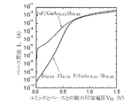
【0024】
図3に示すように、エミッタがInPから構成された従来の状態を示す点線に比較し、エミッタ層をIn(0.85)Al(0.15)Pから構成した場合、実線で示すように、Alの組成が15%と低く抑えられているにもかかわらず、特性が大幅に改善されている。なお、図3は、In(0.85)Al(0.15)Pよりなるエミッタ層を用いたヘテロ接合バイポーラトランジスタとInPよりなるエミッタ層を用いたヘテロ接合バイポーラトランジスタとのガンメル・プロット(gummel-plot)のうち、ベース電流IBを比較したものである。
【0025】
次に、エミッタ層を構成するInAlPの組成、及びベース層を構成するGaAsSbの組成について説明する。以降では、以下の(a),(b),(c),(d)に示す観点から、前述した特性がより効果的に得られる組成について説明する。
(a)組成を格子整合の点からずらしたことによる臨界膜厚の減少と、素子特性から要求される膜厚との関係。
(b)ΔEcが減少する組成の組み合わせ。
(c)GaAsSbの水素不活性化耐性と歪みとの関係。
(d)歪み層同士の相互作用による臨界膜厚の減少、界面での欠陥発生。
【0026】
まず、(a)の観点について説明する。InPからなる基板の上に形成されたGaAs(x)Sb(1-x)は、格子定数の不整合から0.51<x≦1で引っ張り歪みを、0≦x<0.51で圧縮歪みを受ける。また、In(1-y)Al(y)Pは、y>0である限り引っ張り歪みを受ける。歪み層の膜厚は、一般に臨界膜厚以上には厚くすることができない。一方で、以下の理由から薄層化には限界がある。GaAs(x)Sb(1-x)ベース層は、結晶品質の劣化を生じないドーピング濃度が、炭素ドープの場合において4×1020cm3程度までである。このため、ヘテロ接合バイポーラトランジスタの高速化のためにベース抵抗を下げようとすると、例えばベース抵抗が600Ω/口(平方cm)の場合には、膜厚が15nm前後となる。
【0027】
また、In(1-y)Al(y)Pエミッタ層については、薄くした場合にIn(1-y)Al(y)Pエミッタ層のバンドベンディングが急峻になる。このため、GaAsSbベース層の価電子帯端及びエミッタ/ベース界面にIn(1-y)Al(y)P層の伝導帯が近づき、トンネル再結合電流の増加が顕著となる。よって、In(1-y)Al(y)Pエミッタ層についても薄膜化には限界がある。これらのように、GaAs(x)Sb(1-x)からなるベース層及びIn(1-y)Al(y)Pからなるエミッタ層ともに、臨界膜厚以下で、かつ素子特性が劣化しない程度の厚さを持つ状態に形成されていなければならない。この条件を満たす条件としては、組成xの範囲が0.2≦x≦0.8であり、yの範囲が0<y≦0.5であればよい。
【0028】
次に、(b)の観点について説明する。前述した本発明の効果を得るためには、ΔEcがGaAs(0.51)Sb(0.49)/InPの場合よりも減少する必要がある。InPの伝導帯のポテンシャルに対するGaAs(x)Sb(1-x)のポテンシャルとの差、及びIn(1-y)Al(y)のポテンシャルとの差は、組成x及びyによって見積もることが可能である。GaAs(0.51)Sb(0.49)/InPのΔEcについては、約0.18eVと見積もられていることから、組成xとyによってΔEcが0.18eV以下になる条件を求めると、0.49x+1.554y≧0.25となる。
【0029】
前述した(a)の観点及び上述した(b)の観点に加えて、特に本発明の効果を発揮させるためには、ΔEcが0近傍、もしくはエミッタ層側の伝導帯のポテンシャルの方が高くなる条件(0.49x+1.554y≧0.36)を用いるのが望ましい。この条件下で、以降に示す(c)の観点及び(d)の観点から、ヘテロ接合バイポーラトランジスタの高速動作に悪影響を与えない組成の範囲について、さらに検討を行う。
【0030】
(c)の観点について説明すると、まず、As組成xをx≧0.51よりも大きくすると、GaAs(x)Sb(1-x)層は引っ張り歪みを受け、水素不活性化耐性が低下する。実用上無視可能な水素不活性化の度合いは、炭素ドープされたGaAs(x)Sb(1-x)層内に存在する全炭素アクセプタに対し、水素不活性化された炭素アクセプタの割合がおおむね5%以内に抑えられているときである。この条件は、GaAs(x)Sb(1-x)層の組成でみると、x<0.55までなら許容範囲に収めることが可能である。これが、水素不活性化耐性から見たGaAs(x)Sb(1-x)層の組成の上限となる。
【0031】
次に、(d)の観点について説明すると、まず、0≦x<0.51の範囲では、In(1-y)Al(y)P/GaAs(x)Sb(1-x)のΔEcは、xが小さくなるにつれてGaAsSbの伝導帯のポテンシャルが高くなるために大きくなる。この場合、yを大きくすることにより補償することが可能である。この際には、GaAs(x)Sb(1-x)層の圧縮歪みとIn(1-y)Al(y)P層の引っ張り歪みとの相互作用から、臨界膜厚がInP基板の上のときよりも低下し、さらにはエミッタ/ベース界面の欠陥密度が増加する原因となる。これが、歪み層の相互作用から見たGaAs(x)Sb(1-x)層の組成の下限と、In(1-y)Al(y)P層の組成の上限である。
【0032】
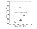
以上の(a),(b),(c),(d)の観点から導き出される条件をまとめて示したものが、図4の説明図である。図4に示すように、領域401で示す条件の範囲が、発明の効果が賢慮に現れる領域である。また、領域402で示す領域が、発明の効果が得られる領域である。また、領域403は、エミッタ/ベース間の伝導帯端不連続量(ΔEc)が、エミッタをInPから構成した場合よりも増加する領域である。また、領域404は、形成される膜の歪みが強いために実用的な膜厚で素子(ヘテロ接合バイポーラトランジスタ)が設計できない領域である。
【0033】
また、さらに、歪みの影響を低減し、かつエミッタ層側の伝導帯のポテンシャル高さをより高めるための方法として、ベース接合面に近いIn(1-y)Al(y)Pエミッタ層のAl組成に対して、ベース接合面(ベース層の側)から遠ざかるにつれてAl組成を減少させてInPに近づける組成傾斜層の適用が考えられる。
【0034】
ところで、GaAsSbからなるベース層におけるAsの組成が、エミッタ層の側から遠ざかるにつれて小さくなるようにしてもよい。このようにすることで、ベース層における伝導帯端が、エミッタ層から遠ざかるにつれてポテンシャルが低くなり、この傾斜により発生した内部電界により、ベース層の少数キャリアが加速されるようになる。このことにより、ベース層における少数キャリアの再結合確率が減少し、電流利得をより向上させることができるとともに、素子の動作速度も向上させることが可能となる。
【0035】
次に、本発明の実施の形態における他のヘテロ接合バイポーラトランジスタについて、図5A及び図5Bを用いて説明する。図5Aは、本発明の実施の形態における他のヘテロ接合バイポーラトランジスタの構成例を示す断面図、図5Bは平面図である。図5A及び図5Bに示すヘテロ接合バイポーラトランジスタは、不純物として鉄(Fe)がドープされて高抵抗とされたInPからなる主表面が(100)とされた基板501の上に、高濃度にシリコン(Si)がドープされてn型とされたInPからなるサブコレクタ層502、InPからなるコレクタ層503、高濃度に炭素(C)がドープされてp型とされたGaAs(0.51)Sb(0.49)からなるベース層504、Siがドープされてn型とされたIn(0.85)Al(0.15)Pからなるエミッタ層507、高濃度にSiがドープされてn型とされたInPからなるキャップ層508、高濃度にSiがドープされてn型とされたIn(0.53)Ga(0.47)Asからなるコンタクト層509が積層されている。
【0036】
また、サブコレクタ層502の上のコレクタ層503が形成されていない領域にオーミック接続したコレクタ電極506が形成され、ベース層504の上のエミッタ層507が形成されていない領域にオーミック接続したベース電極505が形成され、コンタクト層509の上にオーミック接続したエミッタ電極510が形成されている。
なお、サブコレクタ層502は、例えば、Siが2×1019cm-3ドープされ、ベース層504は、例えばCが1.1×1020cm-3ドープされ、エミッタ層507は、例えばSiが5×1017cm-3ドープされ、キャップ層508は、例えばSiが2×1019cm-3ドープされ、コンタクト層509は、例えばSiが3×1019cm-3ドープされている。コレクタ層503は、膜厚150nm程度に形成され、ベース層504は、膜厚20nm程度に形成され、エミッタ層507は、膜厚30nm程度に形成されている。
【0037】
なお、上述した図5A及び図5Bに示すヘテロ接合バイポーラトランジスタの詳細な構造については、説明に支障のない範囲で省略している。また、ドーパント及び各層の構成材料については、上述したものに限定されることなく、所定の素子動作を実現できる物であれば他の材料でもかまわない。
【0038】
次に、図5A及び図5Bに示すヘテロ接合バイポーラトランジスタの製造方法例について簡単に説明する。まず、例えば、MBE法やMOCVD法などの、公知の結晶成長技術(装置)により、前述した各化合物半導体の層が、基板501の上に順次に形成(積層)された状態とする。特に、MOCVD法によりベース層504以降の層を形成する場合は、水素によるCアクセプタの不活性化が極力抑制されるように、成膜時の基板温度は480℃以上の条件とすることが望ましい。なお、MOCVD法でコレクタ層503まで形成した後、MBE法によりベース層504以降の層を形成する場合など、ベース層504中のCアクセプタの不活性化が抑制されている場合は、上記基板温度以下の条件とすることも可能である。
【0039】
次に、公知のリソグラフィ技術とエッチング技術とにより、図5Aに示すようなメサ構造が形成された状態とする。このメサ構造の形成において、本発明の趣旨に反しない状態であれば、エッチング処理においてより高い選択性を得るために、エッチングストッパー層などを用いるようにしてもよい。
【0040】
次に、電極形成部に開口を備えたマスクパターンをリソグラフィにより形成し、このマスクパターンの上よりTi/Pt/Auを蒸着し、この後、マスクパターンを除去(リフトオフ)することで、ベース電極505,コレクタ電極506,エミッタ電極510が形成された状態とする。これらの電極の積層構造については、各電極において下層との間でオーミックコンタクトが取れる状態であれば、他の材料を用いるようにしてもよく、各電極で各々異なる形態としてもよい。
【0041】
上述したように形成された図5A及び図5Bに示すヘテロ接合バイポーラトランジスタによれば、エミッタ層507がInAlPより構成されているため、前述した図1に示すヘテロ接合バイポーラトランジスタと同様に、伝導帯端において、エミッタ層507とベース層504の界面では、エミッタ層507の方が高いポテンシャルを持つ状態となる。この結果、従来ではエミッタ/ベース界面近傍に存在していた障壁が、図5A及び図5Bに示すヘテロ接合バイポーラトランジスタによれば、解消された状態となる。
【0042】
この結果、図5A及び図5Bに示すヘテロ接合バイポーラトランジスタによれば、エミッタ/ベース界面近傍での電子蓄積は抑制され、エミッタ/ベース界面の容量成分が減少する。また、同時にエミッタ層507側の伝導帯とベース層504側の価電子帯との差が大きくなるため、エミッタ/ベース界面でのトンネル再結合電流が減少する。これらの結果、図5A及び図5Bに示すヘテロ接合バイポーラトランジスタにおいても、従来に比較して電流利得が増加するようになる。
【0043】
図6に示すように、エミッタがInPから構成された従来の状態を示す点線に比較し、エミッタ層をInAlPから構成した場合、実線で示すように、Alの組成が15%と低く抑えられているにもかかわらず、特性が大幅に改善されている。なお、図6は、In(0.85)Al(0.15)Pよりなるエミッタ層を用いたヘテロ接合バイポーラトランジスタとInPよりなるエミッタ層を用いたヘテロ接合バイポーラトランジスタとのガンメル・プロット(gummel-plot)のうち、ベース電流IBを比較した特性図である。
【0044】
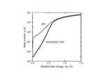
また、図5A及び図5Bに示すヘテロ接合バイポーラトランジスタによれば、図7に示すように、エミッタにInPを用いた従来に比較して、電流利得特性が全体的に向上し、ヘテロ接合バイポーラトランジスタの特性が大幅に改善されるようになる。なお、図7は、コレクタ電流IC−電流利得特性を示したものである。
【0045】
次に、本発明の実施の形態における他のヘテロ接合バイポーラトランジスタについて、図8を用いて説明する。図8は、本発明の実施の形態における他のヘテロ接合バイポーラトランジスタの構成例を示す断面図である。図8に示すヘテロ接合バイポーラトランジスタは、不純物として鉄(Fe)がドープされて高抵抗とされたInPからなる主表面が(100)とされた基板801の上に、高濃度にシリコン(Si)がドープされてn型とされたInPからなるサブコレクタ層802、InPからなるコレクタ層803、高濃度に炭素(C)がドープされてp型とされたGaAs(0.51)Sb(0.49)からなるベース層804、Siがドープされてn型とされてInとAlの組成が層厚方向に変化しているInAlPからなるエミッタ層807、高濃度にSiがドープされてn型とされたInPからなるキャップ層808、高濃度にSiがドープされてn型とされたIn(0.53)Ga(0.47)Asからなるコンタクト層809が積層されている。エミッタ層807は、ベース層804の側からキャップ層808の側にかけて、Inの組成比が0.75から1.00へと変化し、Alの組成比が0.25から0へと変化した、Inが増加してAlが減少する傾斜組成の状態とされている。
【0046】
また、サブコレクタ層802の上のコレクタ層803が形成されていない領域にオーミック接続したコレクタ電極806が形成され、ベース層804の上のエミッタ層807が形成されていない領域にオーミック接続したベース電極805が形成され、コンタクト層809の上にオーミック接続したエミッタ電極810が形成されている。
【0047】
なお、サブコレクタ層802は、例えば、Siが2×1019cm-3ドープされ、ベース層804は、例えばCが7×1019cm-3ドープされ、エミッタ層807は、例えばSiが5×1017cm-3ドープされ、キャップ層808は、例えばSiが1×1019cm-3ドープされ、コンタクト層809は、例えばSiが1.5×1019cm-3ドープされている。コレクタ層803は、膜厚180nm程度に形成され、ベース層804は、膜厚20nm程度に形成され、エミッタ層807は、膜厚30nm程度に形成されている。
【0048】
なお、上述した図8に示すヘテロ接合バイポーラトランジスタの詳細な構造については、説明に支障のない範囲で省略している。また、ドーパント及び各層の構成材料については、上述したものに限定されることなく、所定の素子動作を実現できる物であれば他の材料でもかまわない。また、図8に示すヘテロ接合バイポーラトランジスタは、前述した図1,図5A及び図5Bに示すヘテロ接合バイポーラトランジスタと同様に製造可能である。
【0049】
上述したように形成された図8に示すヘテロ接合バイポーラトランジスタによれば、エミッタ層807がInAlPより構成されているため、前述した図1に示すヘテロ接合バイポーラトランジスタと同様に、伝導帯端において、エミッタ層807とベース層804の界面では、エミッタ層807の方がポテンシャルが高くなる。この結果、従来ではエミッタ/ベース界面近傍に存在していた障壁が、図8に示すヘテロ接合バイポーラトランジスタによれば、解消された状態となる。
【0050】
この結果、図8に示すヘテロ接合バイポーラトランジスタによれば、エミッタ/ベース界面近傍での電子蓄積は抑制され、エミッタ/ベース界面の容量成分が減少する。また、同時にエミッタ層807側の伝導帯とベース層804側の価電子帯との差が大きくなるため、エミッタ/ベース界面でのトンネル再結合電流が減少する。これらの結果、図8に示すヘテロ接合バイポーラトランジスタにおいても、従来に比較して電流利得が増加するようになる。
【0051】
また、図8に示すヘテロ接合バイポーラトランジスタによれば、前述したようにエミッタ層807が傾斜組成とされ、ベース層804との界面においてはAlの組成比が高く、キャップ層808の側に近いほどAlの組成比が低下しているので、Alの組成比が高いことによる歪みの問題が緩和されるようなる。
【0052】
図9に示すように、エミッタがInPから構成された従来の状態を示す点線に比較し、エミッタ層を上述した傾斜組成のInAlPから構成した場合、実線で示すように、特性が大幅に改善されている。また、同様に傾斜組成としてベース層との界面においてはIn(0.85)Al(0.15)Asの組成とされたエミッタ層の場合(2点鎖線)との比較から明らかなように、ベース層に近い領域のエミッタ層のAl組成比が高いほど、低電圧領域において再結合電流成分が抑制されている。なお、図9は、InAlPよりなるエミッタ層を用いたヘテロ接合バイポーラトランジスタ及びInPよりなるエミッタ層を用いたヘテロ接合バイポーラトランジスタとのガンメル・プロット(gummel-plot)のうち、ベース電流IBを比較した特性図である。
【0053】
また、図8に示すヘテロ接合バイポーラトランジスタによれば、図10に示すように、エミッタにInPを用いた従来に比較して、電流利得特性が全体的に向上し、ヘテロ接合バイポーラトランジスタの特性が大幅に改善されるようになる。また、図8に示すヘテロ接合バイポーラトランジスタによれば、ベース層に近い領域のエミッタ層のAl組成比が低い場合に比較しても、電流利得が高くなっている。これは、Alの組成比が高いことにより、エミッタからベースへの電子の打ち出し効果が加わったためと考えられる。以上のように、ベース層に近い領域のAlの組成比が高くされている傾斜組成とされたエミッタ層を用いることで、電流利得の向上という効果がより顕著に得られるようになる。
【0054】
次に、本発明の実施の形態における他のヘテロ接合バイポーラトランジスタについて、図11を用いて説明する。図11は、本発明の実施の形態における他のヘテロ接合バイポーラトランジスタの構成例を示す断面図である。 図11に示すヘテロ接合バイポーラトランジスタは、不純物として鉄(Fe)がドープされて高抵抗とされたInPからなる主表面が(100)とされた基板1101の上に、高濃度にシリコン(Si)がドープされてn型とされたInPからなるサブコレクタ層1102、InPからなるコレクタ層1103、InAlPからなるコレクタ傾斜組成層1104、高濃度に炭素(C)がドープされてp型とされたGaAs(0.51)Sb(0.49)からなるベース層1105、Siがドープされてn型とされてInとAlの組成が層厚方向に変化しているInAlPからなるエミッタ層1108、高濃度にSiがドープされてn型とされたInPからなるキャップ層1109、高濃度にSiがドープされてn型とされたIn(0.53)Ga(0.47)Asからなるコンタクト層1110が積層されている。
【0055】
また、コレクタ傾斜組成層1104は、コレクタ層1103の側からベース層1105の側にかけて、Inの組成比が1.00から0.92へと変化し、Alの組成比が0から0.08へと変化した、Inが減小してAlが増加する傾斜組成の状態とされている。また、エミッタ層1108は、ベース層1105の側からキャップ層1109の側にかけて、Inの組成比が0.75から1.00へと変化し、Alの組成比が0.25から0へと変化した、Inが増加してAlが減少する傾斜組成の状態とされている。
【0056】
また、サブコレクタ層1102の上のコレクタ層1103が形成されていない領域にオーミック接続したコレクタ電極1107が形成され、ベース層1105の上のエミッタ層1108が形成されていない領域にオーミック接続したベース電極1106が形成され、コンタクト層1110の上にオーミック接続したエミッタ電極1111が形成されている。
【0057】
なお、サブコレクタ層1102は、例えば、Siが2×1019cm-3ドープされ、ベース層1105は、例えばCが7×1019cm-3ドープされ、エミッタ層1108は、例えばSiが5×1017cm-3ドープされ、キャップ層1109は、例えばSiが1×1019cm-3ドープされ、コンタクト層1110は、例えばSiが1.5×1019cm-3ドープされている。コレクタ層1103は、膜厚1110nm程度に形成され、コレクタ傾斜組成層1104は、膜厚30nm程度に形成され、ベース層1105は、膜厚20nm程度に形成され、エミッタ層1108は、膜厚30nm程度に形成されている。
【0058】
なお、上述した図11に示すヘテロ接合バイポーラトランジスタの詳細な構造については、説明に支障のない範囲で省略している。また、ドーパント及び各層の構成材料については、上述したものに限定されることなく、所定の素子動作を実現できる物であれば他の材料でもかまわない。また、図11に示すヘテロ接合バイポーラトランジスタは、前述した図1,図5A及び図5B,図8に示すヘテロ接合バイポーラトランジスタと同様に製造可能である。
【0059】
上述した構成の図11に示すヘテロ接合バイポーラトランジスタによれば、まず、エミッタ層1108がInAlPより構成されているため、前述した図1,図5A,及び図8に示すヘテロ接合バイポーラトランジスタと同様に、伝導帯端において、エミッタ層1108とベース層1105の界面では、エミッタ層1108の方がポテンシャルが高くなる。この結果、従来ではエミッタ/ベース界面近傍に存在していた障壁が、図8に示すヘテロ接合バイポーラトランジスタによれば、解消された状態となる。
【0060】
この結果、図11に示すヘテロ接合バイポーラトランジスタにおいても、エミッタ/ベース界面近傍での電子蓄積は抑制され、エミッタ/ベース界面の容量成分が減少する。また、同時にエミッタ層1108側の伝導帯とベース層1105側の価電子帯との差が大きくなるため、エミッタ/ベース界面でのトンネル再結合電流が減少する。これらの結果、図11に示すヘテロ接合バイポーラトランジスタにおいても、従来に比較して電流利得が増加するようになる。
【0061】
また、図11に示すヘテロ接合バイポーラトランジスタにおいても、前述したようにエミッタ層1108が傾斜組成とされ、ベース層1105との界面においてはAlの組成比が高く、キャップ層1109の側に近いほどAlの組成比が低下している。この結果、Alの組成比が高いことによる歪みの問題が緩和されるようになり、図8に示したヘテロ接合バイポーラトランジスタと同様に、より高い電流利得が得られるようになる。
【0062】
加えて、図11に示すヘテロ接合バイポーラトランジスタでは、ベース1105に接する領域におけるコレクタの組成が、InAlPから構成されているようにした。このことにより、以下に説明するコレクタ/ベース界面に生じる境界層の問題が抑制できるようになる。
【0063】
Sbを含む化合物半導体は、他のV族原子であるPやAsなどのみにより構成された化合物半導体よりも融点が低く、例えば2つの元素からなる化合物半導体の場合、GaP(1467℃)、InP(1060℃)、GaAs(1240℃)、InAs(942℃)に対して、GaSb(712℃)、InSb(524℃)となる。また、GaAsSbの一般的な成長温度域は500〜600℃である。これに対し、InSbの融点が低いために、InPとGaAsSbとの接触界面でInSbが形成されるとInP/GaAsSb界面が一時的に液相に近い状態となる("Growth Monitoring of GaAsSb:C/InP Heterostructure with Reflectance Anisotropy Spectroscopy"、F.Brunnerら4名、TMS、Abstract of 12th ICMOVPE、2004年発行、p.2参照)。このような状態になると、急峻に層が切り替わらず、界面を挟んだ両層の構成元素が無頓着に入り交じった境界層が界面に生じてしまう。このような境界層が存在すると、素子構造を形成するために各層を選択的にエッチングしようとしたときに、エッチングが速やかに進行しない、もしくは異常に進行してしまうために、設計通りの素子形状に加工できないという問題を生じる。
【0064】
またこの層は、局所的に強い歪みを生じて転移欠陥を発生させ、また界面近傍の伝導帯端や価電子帯端のポテンシャルを局所的に上下させる。例えば、GaAsSb/InP界面において、InSbを主成分とする境界層ができた場合、図12に示すような伝導帯端の局所的な落ち込みを生じる。この結果、欠陥を介した再結合電流が増加して電流利得が低下し、また伝導帯端の落ち込みや隆起により、コレクターベース間における電子の走行が妨げられ、素子の動作速度が低下するなどの素子特性の劣化をまねく。
【0065】
このような問題を解決するためには、一般には、層から層への原子拡散(例えば、InP層からGaAsSb層へのIn拡散、もしくはGaAsSb層からInP層へのSbの拡散)を防ぐことが重要である。しかしながら、InP/GaAsSb系の場合、潜在的にInPとGaAsSbの接触面にはかならずIn−Sb結合が形成されてしまうために、拡散を抑えるだけでは完全な解決には至らない。また、GaAsSbからなるベース層の成長温度をInSbの融点よりも低くすることにより、InPからなるコレクタ層とベース層(GaAsSb)の接触面にIn−Sb結合が形成されても、界面が液相にならないようにすることも考えられる。
【0066】
しかしながらこの場合、低温成長によりGaAsSbからなるベース層の結晶品質の低下を生じやすいほか、MOCVDにて層構造を作製する場合、炭素ドープしたGaAsSb中の炭素アクセプタの水素不活性化耐性を大きく損なうという新たな問題を生じる(文献「Suppression of hydrogen passivation in carbon-doped GaAsSb grows by MOCVD」、Y.Odaら6名、ELSEVIER、Journal of Crystal Growth、2004年発行、Vol.261、p.393.参照)。
【0067】
これらに対し、図11に示すヘテロ接合バイポーラトランジスタによれば、ベース層1105が形成される下層に、InAlPからなるコレクタ傾斜組成層1104を備え、ベース層1105がInAlPからなる層の上に形成されるようにした。この結果、InとSbからなる境界層の形成が抑制できるようになる。以下、境界層の抑制についてより詳細に説明する。
[0068] 前述したように、Sbを含む化合物半導体は、融点が低い傾向にあるが、Alを含む化合物半導体は、融点が高い傾向になる。例えば、AlP(1060℃前後で昇華)、AlAs(1740℃)、AlSb(1080℃)である。また、原子の結合エネルギーは、Al−Sb>Ga−Sb>In−Sbの順に大きく、Al−Sbが最も安定する。このため、コレクタ層とベース層との界面にアルミを含む化合物半導体を挿入するか、もしくはコレクタ層をIn(1−z)Al(z)P(ただしz>0)から構成することで、界面ではIn−Sb結合よりもAl−Sb結合の方が優先的に形成されることになる。このようにすることで、ベース層のコレクタ側の界面では、融点の低いInSbではなく、融点が高いInAlSbが形成されることとなり、GaAsSbを成長させている初期の段階で、界面が一時的に液相になることを抑えることが可能となる。
[0069] ただし、Alを含む化合物半導体は融点が高いだけでなく、伝導帯端のポテンシャルも高くなる傾向があるため、むやみにAlを添加するとコレクタ層の伝導帯端のポテンシャルがベース層のポテンシャルよりも高くなる。このような状態は、伝導帯を走行する電子に対して障壁となり、ヘテロ接合バイポーラトランジスタの動作速度を著しく低下させることになる。この問題は、例えばInPに格子整合するInAlAsがAlを含んでいるのにもかかわらず、InAlAsをコレクタ層に適用しにくいことの理由ともなる。
[0070] 以上を踏まえて、本発明が効果的に適用される組成等について以下に示す(i)〜(iv)の観点から説明する。
(i)組成を格子整合の点からずらしたことによる臨界膜厚の減少と、素子特性から要求される膜厚との関係。
(ii)GaAsSbの水素不活性化耐性と歪みとの関係。
(iii)歪み層同士の相互作用による臨界膜厚の減少、界面での欠陥発生。
(iv)伝導帯端のポテンシャルが(コレクタ層<ベース層)となる組成の関係。
[0071] まず、(i)の観点について説明する。InP基板上のGaAs(x)Sb(1−x)は、格子定数の不整合から0.51<x≦1で引っ張り歪みを、0≦x<0.51で圧縮歪みを受ける。In(1−z)Al(z)Pは、z>0である限り引っ張り歪みを受ける。歪み層の膜厚は、一般に臨界膜厚以上には厚くすることができない。しかしながら一方で、以下の理由から薄層化には限界がある。GaAs(x)Sb(1−x)ベース層は、結晶品質の劣化を生じないドーピング濃度が炭素ドープの場合において4×1020cm3程度までである。このため、ヘテロ接合バイポーラトランジスタの高速化のためにベース抵抗を下げようとすると、例えばベース抵抗が600Ω/□(平方cm)、ドーピング濃度4×1020cm3の場合には15nm前後の膜厚が、ドーピング濃度8×1019cm3の場合には35nm前後の膜厚が必要となる。このことから、GaAs(x)Sb(1−x)、In(1−z)Al(z)Pともに臨界膜厚以下で、かつ素子特性が劣化しない程度の厚さを持つ膜が成膜できなければならない。特にxについては、ベース抵抗や膜厚の揺らぎに起因するプロセスマージンなども考慮に入れた膜厚15nmでも臨界に達しない、0.2≦x≦0.8が、臨界膜厚から見た実用的な範囲となる。
[0072] 次に、上記(ii)の観点について説明する。As組成xをx≧0.51よりも大きくすると、GaAs(x)Sb(1−x)層は引っ張り歪みを受け、水素不活性化耐性が低下する。実用上無視可能な水素不活性化の度合いは、炭素ドープされたGaAs(x)Sb(1−x)層内に存在する全炭素アクセプタに対して、水素不活性化された炭素アクセプタの割合がおおむね5%以内に抑えられているときある。これは、GaAs(x)Sb(1−x)層の組成でみると、x≦0.55までなら許容範囲に収めることが可能であることを示している。この条件が、水素不活性化耐性から見たGaAs(x)Sb(1−x)層の組成の上限となる。
[0073] 次に、上記(iii)の観点について説明する。0≦x<0.51の範囲では、In(1−z)Al(z)P/GaAs(x)Sb(1−x)のΔEc(伝導帯端不連続量)は、xが小さくなるにつれてGaAsSbの伝導帯のポテンシャルが高くなるために大きくなる。この場合、さらにzを大きくすることが可能となる。この際には、GaAs(x)Sb(1−x)層の圧縮歪みとIn(1−z)Al(z)P層の引っ張り歪みとの相互作用から、臨界膜厚がInP基板上のときよりも低下し、さらにはコレクタ/ベース界面の欠陥密度が増加する原因となる。これが、歪み層の相互作用から見たGaAs(x)Sb(1−x)層の組成の下限と、In(1−z)Al(z)P層の組成の上限であり、x≧0.40かつz≦0.35である。
[0074] 次に、上記(iv)の観点について説明する。素子特性を劣化させないためには、コレクタ層の伝導帯端のポテンシャルがベース層のポテンシャルよりも低く保たれる必要がある。InPの伝導帯のポテンシャルに対するGaAs(x)Sb(1−x)のポテンシャルとの差、及びIn(1−z)Al(z)Pのポテンシャルとの差は、組成x及びzによって見積もることが可能である。GaAs(0.51)Sb(0.49)/InPの△Ecについては約0.18eVと見積もられていることから、組成xとzを用いてコレクタ層側の伝導帯端のポテンシャルの方が低くなる条件は0.49x+1.554z≦0.36である。このとき、(i)〜(iii)から0.40≦x≦0.55であるから、zの取り得る範囲は0<z≦0.18となる。
[0075] 以上をまとめると、ベース層がGaAs(x)Sb(1−x)より構成され、コレクタ層側のベース層との界面がIn(1−z)Al(z)Pより構成され、組成xおよび組成zの範囲がそれぞれ0.40≦x≦0.55、0<z≦0.18で、xとzの関係が0.49x+1.554z≦0.36となれば、前述した境界層の問題が解消可能となる。さらに、歪みの影響を低減する方法として、ベース接合面に近いIn(1−z)Al(z)Pコレクタ層のAl組成に対して、ベース接合面(ベース層の側)から遠ざかるにつれてAl組成を減少させてInPに近づける、組成傾斜層の適用が考えられる。
[0076] 上述したように、図11に示すヘテロ接合バイポーラトランジスタによれば、コレクタ傾斜組成層1104を設けるようにしたので、ベース/コレクタ界面が急峻に組成が変化する状態となる。この結果、図13のバンド図に示すように、ベース/コレクタ界面近傍における伝導帯端の局所的な落ち込みが抑制され、電子の走行に対して障害がない状態が実現可能となる。
[0077] また、InPからなるコレクタ層の上にGaAsSbからなるベース層が形成されている場合、界面に前述した境界層が形成されているため、図11に示すような構造体を形成するためのウエットケミカルエッチングにおいて、ベース層からコレクタ層にかけて選択的なエッチングに支障をきたす場合が発生する。ベース/コレクタ界面に境界層が存在すると、ベース用、もしくはコレクタ用のどちらのエッチャントでも界面近傍でエッチングの挙動が変わってしまい、設計通りの構造を実現することが難しくなる。
[0078] これに対し、コレクタ層1103,コレクタ傾斜組成層1104,及びベース層1105の積層構造においては、図11に示すような構造体を形成するためのウエットケミカルエッチングにおいて、ベース層1105からコレクタ傾斜組、成層1104,及びコレクタ層1103にかけて、境界層が形成されないため、スムースに選択エッチングが行える。
【産業上の利用可能性】
[0079] 以上に示した本発明によれば、より高速な動作が可能なヘテロ接合バイポーラトランジスタが提供できる。【Technical field】
[0001]
The present invention relates to a heterojunction bipolar transistor having a base made of GaAsSb.
[Background]
[0002]
GaAsSb has attracted attention as a compound semiconductor that serves as a base layer material for an InP heterojunction bipolar transistor (HBT). GaAsSb is GaAs to InP substrate (0.51) Sb (0.49) Lattice matching in the composition of InP / GaAs using GaAsSb as the base (0.51) Sb (0.49) / InP-based HBT can simultaneously achieve excellent high-frequency characteristics and high breakdown voltage characteristics (Reference 1: “300 GHz InP / GaAsSb / InP Doub1e HBTs with High Current Capabi1ity and BVceo ≧ 6V”, MWDvorak, Student Member) IEEE, CRBo1ognesi, Member, IEEE, OJPitts, and SPWatkins, Member, IEEE,: IEEE ELECTRON DEVICE LETTERS, VOL.22, NO.8, AUGUST 2001 p.361.). In the heterojunction, as shown in FIG. CA And valence band E VA Is the conduction band E of semiconductor B CB And valence band E VB And the potential (energy potential) is "E CA > E CB "And" E VA > E VB And a type-I heterojunction as shown in FIG. CA <E CB "And" E VA <E VB And the heterojunction bipolar transistor is composed of a type-II heterojunction.
[0003]
GaAs on base (0.51) Sb (0.49) When this is used, the potential of the conduction band edge becomes higher than the potential of the conduction band edge of the InP collector layer, and the current blocking effect in the collector, which has been a problem in the InGaAs / InP HBT, is eliminated. Thus, excellent high frequency characteristics and high breakdown voltage characteristics can be obtained at the same time. Furthermore, when GaAsSb is applied to the base layer, carbon atoms having a small diffusion coefficient can be doped at a high concentration, which is advantageous for reducing the base parasitic resistance.
[0004]
Even when InGaAs is applied to the base layer, carbon atoms can be used as a p-type dopant. 19 cm −3 The above ultra-high concentration doping is difficult. In addition, when an InGaAs layer is formed by metal organic chemical vapor deposition (MOCVD), which is a general growth method, it has been pointed out that the carbon acceptor is inactivated by hydrogen atoms. This deactivation of carbon acceptors by hydrogen not only degrades the characteristics of the device by increasing the resistance of the base layer, but also changes the resistance value due to the change in the proportion of carbon acceptors that are deactivated during energization. This brings about a burn-in effect such as, and degrades the reliability of the device. GaAsSb is very resistant to this hydrogen deactivation.
DISCLOSURE OF THE INVENTION
[Problems to be solved by the invention]
[0005] However, the following problems remain in the InP / GaAsSb / InP-based HBT. One is excessive accumulation of emitter-injected electrons due to discontinuity of the conduction band edge between the emitter and base, and an increase in emitter junction capacitance due to this. As shown in the band diagram of FIG. 16, the heterojunction between the InP emitter layer and the GaAsSb base layer has a higher potential at the conduction band edge on the base layer side made of p-type GaAsSb than on the emitter layer side made of InP. This band discontinuity can cause excessive electron accumulation in the emitter space charge region. Furthermore, when the forward voltage is increased to allow a high current to flow, a local potential drop occurs at the conduction band edge in the vicinity of the emitter / base interface, further increasing the electron accumulation. Any of these acts as a capacitive component for the element operation, and hinders the high-speed operation of the element. It also causes an increase in the tunnel recombination current via the defect level existing in the vicinity of the emitter / base interface, leading to a decrease in current gain.
[0006] In order to solve these problems, in the InP / GaAsSb-based HBT structure, the conduction band edge discontinuity between the emitter and the base (ΔEc) is reduced and further inverted (the conduction band edge of the emitter is reduced). Potential> base conduction band edge potential). The following two attempts have been made as this method.
(1) The potential of the conduction band edge of the base layer is expressed as GaAs (0.51) Sb (0.49) Lower than.
(2) A material whose conduction band edge potential is higher than that of InP is used for the emitter layer.
[0007] (1) is GaAs (X) Sb (1-x) This can be realized by increasing the As composition x of the base layer to more than 0.51 (for example, Document 2: JP-A-2002-270616). This method can be easily realized basically only by changing the film forming conditions of GaAsSb, but is subject to tensile strain because the lattice constant of GaAsSb is smaller than that of InP. For this reason, when the As composition is increased, the critical thickness of the GaAsSb layer (determined by the thickness exceeding the strain accumulation limit, the degree of lattice mismatch between the substrate and the growth layer, the elastic modulus of the growth layer material, etc.) decreases. When the critical film thickness is exceeded, microcracks occur in the GaAsSb layer. For this reason, there is a limit to the increase in As composition, and ΔEc cannot be made sufficiently small. In addition, the increase in tensile strain causes a new problem that when a layer structure is formed by metal organic chemical vapor deposition (MOCVD), the hydrogen inactivation resistance of carbon acceptors in carbon-doped GaAsSb is greatly impaired. .
[0008]
The above (2) indicates that InP lattice-matched to InP (0.52) Al (0.48) This is a method using As (for example, Document 3: Japanese Patent Laid-Open No. 2002-270615). However, in this material system, the Al composition is as large as 0.48, and the resistance to natural oxidation is much lower than that of InP. In addition to the problem that the n-type doping efficiency of the InAlAs layer is low, InAlAs doped with Si, which is generally used as an n-type dopant, has a problem that carriers are easily inactivated by fluorine (F). is there. Furthermore, in general, when a film containing a large amount of Al is crystal-grown, it is necessary to increase the growth temperature in order to obtain a film having a high crystal quality. ), The temperature difference from the growth temperature of the base layer (on the order of 500 ° C.) increases, and there is a risk of deteriorating crystal quality at the base layer and the base / collector interface. Further, as mentioned in Document 2, there is a problem that it is difficult to obtain a good InAlAs / GaAsSb interface.
[0009]
The present invention has been made to solve the above-described problems. In the state where problems in the manufacturing process such as impurity inactivation and interface deterioration are suppressed, the capacitance in the vicinity of the emitter / base interface is reduced. An object of the present invention is to allow a heterojunction bipolar transistor using GaAsSb as a base to reduce the current gain and to operate at a higher speed by reducing the components.
[Means for Solving the Problems]
[0010]
The heterojunction bipolar transistor according to the present invention is basically a heterojunction bipolar transistor structure having a GaAsSb-based material in the base layer, and a heterojunction composed of a material containing In, Al, and P in at least one layer in the emitter layer. It has a junction bipolar transistor structure, and includes at least Ga, As, and Sb as constituent elements of the compound semiconductor forming the base layer, and includes at least In, Al, and P as constituent elements of the compound semiconductor forming the emitter layer. It is a thing. As a result, the potential of the emitter layer can be made higher at the interface between the emitter layer and the base layer at the conduction band edge.
[0011] A heterojunction bipolar transistor according to the present invention includes a substrate made of InP, a collector layer formed on the substrate and made of a compound semiconductor containing indium and phosphorus, and the collector layer. A base layer made of a p-type compound semiconductor containing gallium, arsenic and antimony and an n-type compound semiconductor containing indium, aluminum and phosphorus formed on the base layer. And a composition ratio of indium and aluminum in the emitter layer such that the potential at the conduction band edge on the base layer side of the emitter layer is equal to or higher than the potential at the conduction band edge of the base layer. It is made to be a ratio.
[0012] In the heterojunction bipolar transistor, at least one of the base layers is GaAs. (X) Sb (1-x) , At least one of the emitter layers is In (1-y) Al (y) P is used, and the above x and y represent mixed crystal compositions, and each composition may be in the range of 0 <x <1, 0 <y <1. The range of the composition x is 0.2 ≦ x ≦ 0.8, and the range of y may be 0 <y ≦ 0.5. Further, the relationship between x and y may be 0.49x + 1.554y ≧ 0.25. In addition, the composition x and y ranges may be 0.45 ≦ x ≦ 0.55 and 0 <y ≦ 0.25, respectively, and the relationship between x and y may be 0.49x + 1.554y ≧ 0.36.
[0013]
In the heterojunction bipolar transistor, the composition ratio of Al in the emitter layer is such that the gradient composition becomes smaller as the distance from the base layer increases. Do . Further, the composition ratio of As in the base layer may be a gradient composition that decreases as the distance from the emitter layer increases.
[0014]
In the above heterojunction bipolar transistor, the collector layer is composed of a compound semiconductor containing indium, aluminum, and phosphorus. And The source layer is GaAs (x) Sb (1-x) Consists of Shi The collector layer is In (1-z) Al (z) Consists of P Shi , X and z represent mixed crystal compositions, and each composition is in the range of 0 <x <1, 0 <z <1. The The range of z is 0 <z ≦ 0.18, and the relationship between x and z may be 0.49x + 1.554z ≦ 0.36. In addition, the Al composition ratio in the collector layer may be a gradient composition that decreases as the distance from the base layer increases.
[0015]
Note that in the heterojunction bipolar transistor, each layer may be formed by a metal organic chemical vapor deposition method, and the base layer may be added with carbon as a dopant. Further, if the base layer is formed at a growth temperature of 480 ° C. or higher, the ratio of the carbon acceptor that is deactivated by hydrogen is suppressed to 15% or lower.
【The invention's effect】
[0016]
As described above, according to the present invention, in the heterojunction bipolar transistor having a GaAsSb-based material in the base layer, the emitter layer is composed of the compound semiconductor composed of indium, aluminum, and phosphorus. ΔEc can be reduced and reversed. As a result, the heterojunction bipolar transistor using GaAsSb as the base, such as reducing the capacitance component of the emitter / base interface and increasing the current amplification factor without impairing the hydrogen inactivation resistance and device reliability of GaAsSb. However, it is possible to obtain an excellent effect that the decrease in current gain is suppressed and the operation becomes faster.
[Brief description of the drawings]
[0017]
FIG. 1 is a schematic cross-sectional view showing a configuration example of a heterojunction bipolar transistor in an embodiment of the present invention.
FIG. 2 is a schematic diagram of a band lineup from an
FIG. 3 shows In (0.85) Al (0.15) Of the Gummel-plot of the heterojunction bipolar transistor using the emitter layer made of P and the heterojunction bipolar transistor using the emitter layer made of InP, the base current I B FIG.
FIG. 4 shows the In of the present invention (L−y) Al (Y) P / GaAs (X) Sb (L−x) It is explanatory drawing which shows the effect range of the invention by the composition x in y.
FIG. 5A is a cross-sectional view showing a configuration example of another heterojunction bipolar transistor in accordance with the exemplary embodiment of the present invention.
FIG. 5B is a plan view showing a configuration example of another heterojunction bipolar transistor according to the exemplary embodiment of the present invention.
FIG. 6 shows In (0.85) Al (0.15) FIG. 6 is a characteristic diagram comparing Gummel plots of a heterojunction bipolar transistor using an emitter layer made of P and a heterojunction bipolar transistor using an emitter layer made of InP.
FIG. 7 shows the collector current I C -A characteristic diagram showing current gain characteristics.
FIG. 8 is a cross-sectional view showing a configuration example of another heterojunction bipolar transistor in the embodiment of the present invention.
FIG. 9 is a characteristic diagram comparing a Gummel plot between a heterojunction bipolar transistor using an emitter layer made of InAlP and a heterojunction bipolar transistor using an emitter layer made of InP.
FIG. 10 is a characteristic diagram showing current gain characteristics of the heterojunction bipolar transistor shown in FIG. 8;
FIG. 11 is a cross-sectional view showing a configuration example of another heterojunction bipolar transistor according to an embodiment of the present invention.
FIG. 12 is a schematic diagram of a band lineup from a base layer to a collector layer when a boundary layer mainly composed of InSb is formed at a GaAsSb / InP interface.
FIG. 13 is a schematic diagram of a band lineup from the base layer to the collector layer in the heterojunction bipolar transistor shown in FIG.
FIG. 14 is a schematic diagram of a type-I band lineup composed of two types of semiconductors.
FIG. 15 is a schematic diagram of a type-II band lineup composed of two types of semiconductors.
FIG. 16 is a schematic diagram of a band lineup at a heterojunction of an InP emitter layer and a GaAsSb base layer.
BEST MODE FOR CARRYING OUT THE INVENTION
[0018]
Hereinafter, embodiments of the present invention will be described with reference to the drawings.
FIG. 1 is a schematic cross-sectional view showing a configuration example of a heterojunction bipolar transistor according to an embodiment of the present invention. The heterojunction bipolar transistor shown in FIG. 1 has a high concentration of silicon (Si) on a
[0019]
Also, a
The subcollector layer 2 is made of, for example, 2 × 10 Si. 19 cm -3 The base layer 4 is doped, for example, C is 1.1 × 10 20 cm -3 The
[0020]
The detailed structure of the heterojunction bipolar transistor shown in FIG. 1 is omitted as long as there is no problem with the description. Further, the dopant and the constituent material of each layer are not limited to those described above, and other materials may be used as long as they can realize a predetermined element operation. For example, Sn can be applied to the dopant as n-type in addition to Si, and Zn, Be, etc. can be applied as p-type in addition to C (carbon).
[0021]
Next, a method for manufacturing the heterojunction bipolar transistor shown in FIG. 1 will be briefly described. First, the above-described compound semiconductor layer is formed by a known crystal growth technique (apparatus) such as MBE (Molecular Beam Epitaxy) or MOCVD (Metal Organic Chemical Vapor Deposition). Are sequentially formed (stacked) on the
[0022]
According to the heterojunction bipolar transistor shown in FIG. 1 formed as described above, the
[0023]
Due to the above-described difference, the barrier that has conventionally existed in the vicinity of the emitter / base interface is eliminated according to the heterojunction bipolar transistor shown in FIG. As a result, according to the heterojunction bipolar transistor shown in FIG. 1, the accumulation of electrons near the emitter / base interface is suppressed, and the capacitance component at the emitter / base interface is reduced. At the same time, since the difference between the conduction band on the
[0024]
As shown in FIG. 3, the emitter layer is made of InP in comparison with the dotted line showing the conventional state in which the emitter is made of InP. (0.85) Al (0.15) In the case of being composed of P, as shown by the solid line, the characteristics are greatly improved even though the Al composition is kept as low as 15%. In addition, FIG. 3 shows In (0.85) Al (0.15) Of the Gummel-plot of the heterojunction bipolar transistor using the emitter layer made of P and the heterojunction bipolar transistor using the emitter layer made of InP, the base current I B Is a comparison.
[0025]
Next, the composition of InAlP constituting the emitter layer and the composition of GaAsSb constituting the base layer will be described. Hereinafter, from the viewpoints shown in the following (a), (b), (c), and (d), a composition capable of more effectively obtaining the above-described characteristics will be described.
(A) Relationship between reduction in critical film thickness due to shift of composition from lattice matching point and film thickness required from device characteristics.
(B) A combination of compositions that reduces ΔEc.
(C) Relationship between resistance to hydrogen deactivation of GaAsSb and strain.
(D) Reduction of critical film thickness due to interaction between strain layers and generation of defects at the interface.
[0026]
First, the viewpoint (a) will be described. GaAs formed on a substrate made of InP (x) Sb (1-x) Are subject to tensile strain when 0.51 <x ≦ 1 and compressive strain when 0 ≦ x <0.51 due to mismatch of lattice constants. Also, In (1-y) Al (y) P undergoes tensile strain as long as y> 0. In general, the strained layer cannot be thicker than the critical thickness. On the other hand, there is a limit to thinning for the following reasons. GaAs (x) Sb (1-x) The base layer has a doping concentration that does not cause deterioration of crystal quality when the doping concentration is 4 × 10 × 10. 20 cm Three To the extent. For this reason, if the base resistance is lowered to increase the speed of the heterojunction bipolar transistor, for example, when the base resistance is 600 Ω / port (square cm), the film thickness is about 15 nm.
[0027]
Also, In (1-y) Al (y) When the P emitter layer is thinned, In (1-y) Al (y) The band bending of the P emitter layer becomes steep. For this reason, the valence band edge and the emitter / base interface of the GaAsSb base layer (1-y) Al (y) The conduction band of the P layer approaches and the tunnel recombination current increases significantly. Therefore, In (1-y) Al (y) There is a limit to thinning the P emitter layer as well. Like these, GaAs (x) Sb (1-x) A base layer and In (1-y) Al (y) Both emitter layers made of P must be formed to have a thickness that is not more than the critical film thickness and does not deteriorate the device characteristics. As conditions for satisfying this condition, the range of the composition x may be 0.2 ≦ x ≦ 0.8, and the range of y may be 0 <y ≦ 0.5.
[0028]
Next, the viewpoint (b) will be described. In order to obtain the effect of the present invention described above, ΔEc is set to GaAs. (0.51) Sb (0.49) It is necessary to reduce it compared with the case of / InP. GaAs for the potential of the conduction band of InP. (x) Sb (1-x) The difference from the potential of In, and In (1-y) Al (y) The difference from the potential can be estimated by the compositions x and y. GaAs (0.51) Sb (0.49) Since ΔEc of / InP is estimated to be about 0.18 eV, when the condition that ΔEc is 0.18 eV or less is determined by the composition x and y, 0.49x + 1.554y ≧ 0.25.
[0029]
In addition to the above-mentioned viewpoint (a) and the above-mentioned viewpoint (b), in particular, ΔEc is near 0 or the potential of the conduction band on the emitter layer side becomes higher in order to exert the effect of the present invention. It is desirable to use the condition (0.49x + 1.554y ≧ 0.36). Under these conditions, from the viewpoints of (c) and (d) described below, the range of the composition that does not adversely affect the high-speed operation of the heterojunction bipolar transistor is further examined.
[0030]
The viewpoint of (c) will be described. First, when the As composition x is larger than x ≧ 0.51, GaAs (x) Sb (1-x) The layer is subjected to tensile strain and the hydrogen deactivation resistance is reduced. The practically negligible degree of hydrogen deactivation is the carbon-doped GaAs (x) Sb (1-x) This is when the ratio of the hydrogen-inactivated carbon acceptor to the total carbon acceptor present in the layer is kept within 5%. This condition is GaAs (x) Sb (1-x) In terms of the composition of the layer, if x <0.55, it is possible to fall within an allowable range. This is GaAs from the standpoint of hydrogen deactivation resistance (x) Sb (1-x) This is the upper limit of the composition of the layer.
[0031]
Next, the viewpoint (d) will be described. First, in the range of 0 ≦ x <0.51, In (1-y) Al (y) P / GaAs (x) Sb (1-x) ΔEc of the GaAsSb increases as x decreases, because the potential of the conduction band of GaAsSb increases. In this case, it is possible to compensate by increasing y. In this case, GaAs (x) Sb (1-x) Compressive strain of layer and In (1-y) Al (y) Due to the interaction with the tensile strain of the P layer, the critical film thickness is lower than that on the InP substrate, and further, the defect density at the emitter / base interface is increased. This is GaAs from the viewpoint of the interaction of the strained layer (x) Sb (1-x) The lower limit of the composition of the layer and In (1-y) Al (y) This is the upper limit of the composition of the P layer.
[0032]
FIG. 4 is an explanatory diagram showing the conditions derived from the above viewpoints (a), (b), (c), and (d). As shown in FIG. 4, the range of the condition indicated by the
[0033]
Furthermore, as a method for reducing the influence of strain and increasing the potential height of the conduction band on the emitter layer side, In is close to the base junction surface. (1-y) Al (y) For the Al composition of the P emitter layer, it is conceivable to apply a composition gradient layer in which the Al composition is reduced to approach InP as the distance from the base junction surface (base layer side) increases.
[0034]
By the way, the composition of As in the base layer made of GaAsSb may be reduced as the distance from the emitter layer side increases. By doing so, the potential of the conduction band edge in the base layer becomes lower as it goes away from the emitter layer, and minority carriers in the base layer are accelerated by the internal electric field generated by this inclination. As a result, the recombination probability of minority carriers in the base layer is reduced, the current gain can be further improved, and the operation speed of the element can be improved.
[0035]
Next, another heterojunction bipolar transistor according to an embodiment of the present invention will be described with reference to FIGS. 5A and 5B. FIG. 5A is a cross-sectional view showing a configuration example of another heterojunction bipolar transistor in the embodiment of the present invention, and FIG. 5B is a plan view. The heterojunction bipolar transistor shown in FIGS. 5A and 5B has a high concentration of silicon on a
[0036]
Further, a
The
[0037]
Note that the detailed structure of the heterojunction bipolar transistor shown in FIGS. 5A and 5B is omitted as long as there is no problem with the description. Further, the dopant and the constituent material of each layer are not limited to those described above, and other materials may be used as long as they can realize a predetermined element operation.
[0038]
Next, an example of a method for manufacturing the heterojunction bipolar transistor shown in FIGS. 5A and 5B will be briefly described. First, the above-described compound semiconductor layers are sequentially formed (laminated) on the
[0039]
Next, a mesa structure as shown in FIG. 5A is formed by a known lithography technique and etching technique. In the formation of this mesa structure, an etching stopper layer or the like may be used in order to obtain higher selectivity in the etching process as long as it does not contradict the gist of the present invention.
[0040]
Next, a mask pattern having an opening in the electrode forming portion is formed by lithography, Ti / Pt / Au is vapor-deposited on the mask pattern, and then the mask pattern is removed (lifted off), whereby the
[0041]
According to the heterojunction bipolar transistor shown in FIGS. 5A and 5B formed as described above, since the
[0042]
As a result, according to the heterojunction bipolar transistor shown in FIGS. 5A and 5B, the electron accumulation near the emitter / base interface is suppressed, and the capacitance component at the emitter / base interface is reduced. At the same time, the difference between the conduction band on the
[0043]
As shown in FIG. 6, when the emitter layer is made of InAlP, the composition of Al is suppressed to a low level of 15% as shown by the solid line, compared to the dotted line showing the conventional state where the emitter is made of InP. Despite the fact that the characteristics have been greatly improved. FIG. 6 shows In (0.85) Al (0.15) Of the Gummel-plot of the heterojunction bipolar transistor using the emitter layer made of P and the heterojunction bipolar transistor using the emitter layer made of InP, the base current I B FIG.
[0044]
Further, according to the heterojunction bipolar transistor shown in FIGS. 5A and 5B, as shown in FIG. 7, the current gain characteristic is improved as a whole as compared with the conventional case where InP is used for the emitter, and the heterojunction bipolar transistor is obtained. The characteristics will be greatly improved. FIG. 7 shows the collector current I C -Current gain characteristics are shown.
[0045]
Next, another heterojunction bipolar transistor in the embodiment of the present invention will be described with reference to FIG. FIG. 8 is a cross-sectional view showing a configuration example of another heterojunction bipolar transistor in the embodiment of the present invention. The heterojunction bipolar transistor shown in FIG. 8 has a high concentration of silicon (Si) on a
[0046]
In addition, a
[0047]
Note that the
[0048]
Note that the detailed structure of the heterojunction bipolar transistor shown in FIG. 8 described above is omitted as long as there is no problem with the description. Further, the dopant and the constituent material of each layer are not limited to those described above, and other materials may be used as long as they can realize a predetermined element operation. Further, the heterojunction bipolar transistor shown in FIG. 8 can be manufactured in the same manner as the heterojunction bipolar transistor shown in FIGS. 1, 5A, and 5B.
[0049]
According to the heterojunction bipolar transistor shown in FIG. 8 formed as described above, since the
[0050]
As a result, according to the heterojunction bipolar transistor shown in FIG. 8, the accumulation of electrons near the emitter / base interface is suppressed, and the capacitance component at the emitter / base interface is reduced. At the same time, the difference between the conduction band on the
[0051]
Further, according to the heterojunction bipolar transistor shown in FIG. 8, the
[0052]
As shown in FIG. 9, when the emitter layer is made of InAlP having the gradient composition described above, the characteristics are greatly improved as shown by the solid line, compared to the dotted line showing the conventional state where the emitter is made of InP. ing. Similarly, the In composition at the interface with the base layer has a gradient composition. (0.85) Al (0.15) As is clear from the comparison with the emitter layer having the composition of As (two-dot chain line), the higher the Al composition ratio of the emitter layer in the region close to the base layer, the lower the recombination current component in the low voltage region. Has been. FIG. 9 shows a base current I of a Gummel-plot of a heterojunction bipolar transistor using an emitter layer made of InAlP and a heterojunction bipolar transistor using an emitter layer made of InP. B FIG.
[0053]
Further, according to the heterojunction bipolar transistor shown in FIG. 8, as shown in FIG. 10, the current gain characteristic is improved as a whole as compared with the conventional technique using InP as the emitter, and the characteristic of the heterojunction bipolar transistor is improved. It will be greatly improved. Further, according to the heterojunction bipolar transistor shown in FIG. 8, the current gain is high even when compared with the case where the Al composition ratio of the emitter layer in the region close to the base layer is low. This is presumably because the electron emission effect from the emitter to the base was added due to the high composition ratio of Al. As described above, by using an emitter layer having a gradient composition in which the Al composition ratio in the region close to the base layer is increased, the effect of improving the current gain can be obtained more significantly.
[0054]
Next, another heterojunction bipolar transistor according to an embodiment of the present invention will be described with reference to FIG. FIG. 11 is a cross-sectional view showing a configuration example of another heterojunction bipolar transistor in the embodiment of the present invention. The heterojunction bipolar transistor shown in FIG. 11 has a high concentration of silicon (Si) on a substrate 1101 whose main surface is made of InP doped with iron (Fe) as an impurity and made high resistance. N-
[0055]
In the collector
[0056]
In addition, a
[0057]
Note that the
[0058]
Note that the detailed structure of the heterojunction bipolar transistor shown in FIG. 11 described above is omitted as long as it does not interfere with the description. Further, the dopant and the constituent material of each layer are not limited to those described above, and other materials may be used as long as they can realize a predetermined element operation. Further, the heterojunction bipolar transistor shown in FIG. 11 can be manufactured in the same manner as the heterojunction bipolar transistor shown in FIG. 1, FIG. 5A, FIG. 5B, and FIG.
[0059]
According to the heterojunction bipolar transistor shown in FIG. 11 having the configuration described above, first, since the
[0060]
As a result, also in the heterojunction bipolar transistor shown in FIG. 11, the accumulation of electrons near the emitter / base interface is suppressed, and the capacitance component at the emitter / base interface decreases. At the same time, since the difference between the conduction band on the
[0061]
Also in the heterojunction bipolar transistor shown in FIG. 11, the
[0062]
In addition, in the heterojunction bipolar transistor shown in FIG. 11, the composition of the collector in the region in contact with the
[0063]
A compound semiconductor containing Sb has a lower melting point than a compound semiconductor composed only of other group V atoms such as P and As. For example, in the case of a compound semiconductor composed of two elements, GaP (1467 ° C.), InP ( 1060 ° C.), GaAs (1240 ° C.), and InAs (942 ° C.), GaSb (712 ° C.) and InSb (524 ° C.). The general growth temperature range of GaAsSb is 500 to 600 ° C. On the other hand, since the melting point of InSb is low, when InSb is formed at the contact interface between InP and GaAsSb, the InP / GaAsSb interface is temporarily close to the liquid phase ("Growth Monitoring of GaAsSb: C / InP Heterostructure with Reflectance Anisotropy Spectroscopy ", F. Brunner et al., 4 persons, see TMS, Abstract of 12th ICMOVPE, 2004, p. In such a state, the layers are not switched suddenly, and a boundary layer is formed at the interface where the constituent elements of both layers sandwiching the interface are inadvertently mixed. If such a boundary layer exists, when the layers are selectively etched to form an element structure, the etching does not proceed quickly or abnormally, so that the element shape as designed. This causes a problem that it cannot be processed.
[0064]
In addition, this layer generates a strong strain locally to generate a transition defect, and locally raises and lowers the potential at the conduction band edge and the valence band edge near the interface. For example, when a boundary layer composed mainly of InSb is formed at the GaAsSb / InP interface, a local drop in the conduction band edge as shown in FIG. 12 occurs. As a result, the recombination current through the defect increases and the current gain decreases, and the conduction and the rise of the conduction band edge impedes the movement of electrons between the collector base and the device operation speed. Deterioration of device characteristics.
[0065]
In order to solve such a problem, it is generally to prevent atomic diffusion from layer to layer (for example, In diffusion from InP layer to GaAsSb layer, or Sb diffusion from GaAsSb layer to InP layer). is important. However, in the case of the InP / GaAsSb system, since an In—Sb bond is always formed on the contact surface between InP and GaAsSb, it is not possible to completely solve the problem only by suppressing diffusion. Also, by making the growth temperature of the base layer made of GaAsSb lower than the melting point of InSb, even if an In—Sb bond is formed at the contact surface between the collector layer made of InP and the base layer (GaAsSb), the interface becomes a liquid phase. It may be possible not to become.
[0066]
However, in this case, the crystal quality of the base layer made of GaAsSb is likely to deteriorate due to low temperature growth, and when the layer structure is formed by MOCVD, the hydrogen deactivation resistance of the carbon acceptor in the carbon-doped GaAsSb is greatly impaired. A new problem arises (refer to the document “Suppression of hydrogen passage in carbon-doped GaAsSb growth by MOCVD”, Y. Oda et al., 6 names, ELSEVIER, Journal of Crystal Gol. .
[0067]
On the other hand, according to the heterojunction bipolar transistor shown in FIG. 11, the collector
[0068] As described above, the compound semiconductor containing Sb tends to have a low melting point, whereas the compound semiconductor containing Al tends to have a high melting point. For example, AlP (sublimation around 1060 ° C.), AlAs (1740 ° C.), AlSb (1080 ° C.). Moreover, the bond energy of atoms is large in the order of Al—Sb>Ga—Sb> In—Sb, and Al—Sb is most stable. Therefore, a compound semiconductor containing aluminum is inserted at the interface between the collector layer and the base layer, or the collector layer is made of In (1-z) Al (Z) By configuring from P (however, z> 0), the Al—Sb bond is formed preferentially at the interface over the In—Sb bond. In this way, InAlSb having a high melting point is formed at the interface on the collector side of the base layer instead of InSb having a low melting point, and at the initial stage of growing GaAsSb, the interface temporarily It becomes possible to suppress becoming a liquid phase.
[0069] However, since a compound semiconductor containing Al not only has a high melting point, but also tends to have a high potential at the conduction band edge, if Al is added unnecessarily, the potential at the conduction band edge of the collector layer becomes the potential of the base layer. Higher than. Such a state becomes a barrier against electrons traveling in the conduction band, and significantly reduces the operating speed of the heterojunction bipolar transistor. This problem is also a reason why it is difficult to apply InAlAs to the collector layer even though InAlAs lattice-matched to InP contains Al, for example.
[0070] Based on the above, the composition and the like to which the present invention is effectively applied will be described from the following viewpoints (i) to (iv).
(I) The relationship between the decrease in critical film thickness due to shifting the composition from the point of lattice matching and the film thickness required from the device characteristics.
(Ii) Relationship between hydrogen deactivation resistance and strain of GaAsSb.
(Iii) Reduction of critical film thickness due to interaction between strain layers and generation of defects at the interface.
(Iv) A compositional relationship in which the potential at the conduction band edge is (collector layer <base layer).
[0071] First, the aspect (i) will be described. GaAs on InP substrate (X) Sb (1-x) Is subjected to tensile strain when 0.51 <x ≦ 1 due to mismatch of lattice constants and compressive strain when 0 ≦ x <0.51. In (1-z) Al (Z) P undergoes tensile strain as long as z> 0. In general, the strained layer cannot be thicker than the critical thickness. On the other hand, however, there is a limit to thinning for the following reasons. GaAs (X) Sb (1-x) The base layer is 4 × 10 4 when the doping concentration that does not cause deterioration of crystal quality is carbon doping. 20 cm 3 To the extent. For this reason, if the base resistance is lowered to increase the speed of the heterojunction bipolar transistor, for example, the base resistance is 600Ω / □ (square cm), and the doping concentration is 4 × 10. 20 cm 3 In this case, the film thickness around 15 nm has a doping concentration of 8 × 10. 19 cm 3 In this case, a film thickness of about 35 nm is required. From this, GaAs (X) Sb (1-x) , In (1-z) Al (Z) It is necessary to be able to form a film having a thickness that is less than the critical film thickness for both P and does not deteriorate the device characteristics. In particular, for x, the criticality is not reached even at a film thickness of 15 nm that takes into account the process margin caused by the base resistance and the fluctuation of the film thickness. Range.
[0072] Next, the aspect (ii) will be described. When the As composition x is larger than x ≧ 0.51, GaAs (X) Sb (1-x) The layer is subjected to tensile strain and the hydrogen deactivation resistance is reduced. The practically negligible degree of hydrogen deactivation is the carbon-doped GaAs (X) Sb (1-x) There are times when the ratio of hydrogen-inactivated carbon acceptors to the total carbon acceptors present in the layer is kept within 5%. This is GaAs (X) Sb (1-x) In terms of the composition of the layer, it is shown that it is possible to fall within an allowable range up to x ≦ 0.55. This condition is GaAs from the standpoint of hydrogen deactivation resistance. (X) Sb (1-x) This is the upper limit of the composition of the layer.
[0073] Next, the aspect (iii) will be described. In the range of 0 ≦ x <0.51, In (1-z) Al (Z) P / GaAs (X) Sb (1-x) ΔEc (conduction band edge discontinuity amount) of the GaAsSb increases as the potential of the conduction band of GaAsSb increases as x decreases. In this case, z can be further increased. In this case, GaAs (X) Sb (1-x) Compressive strain of layer and In (1-z) Al (Z) Due to the interaction with the tensile strain of the P layer, the critical film thickness becomes lower than that on the InP substrate, and further, the defect density at the collector / base interface increases. This is GaAs from the viewpoint of the interaction of the strained layer (X) Sb (1-x) The lower limit of the composition of the layer and In (1-z) Al (Z) It is the upper limit of the composition of the P layer, and x ≧ 0.40 and z ≦ 0.35.
[0074] Next, the aspect (iv) will be described. In order not to deteriorate the device characteristics, the potential of the conduction band edge of the collector layer needs to be kept lower than the potential of the base layer. GaAs for the potential of the conduction band of InP. (X) Sb (1-x) The difference from the potential of In, and In (1-z) Al (Z) The difference from the potential of P can be estimated by the compositions x and z. GaAs (0.51) Sb (0.49) Since ΔEc of / InP is estimated to be about 0.18 eV, the condition that the potential of the conduction band edge on the collector layer side becomes lower using the composition x and z is 0.49x + 1.554z ≦ 0 .36. At this time, since 0.40 ≦ x ≦ 0.55 from (i) to (iii), the possible range of z is 0 <z ≦ 0.18.
[0075] In summary, the base layer is GaAs (X) Sb (1-x) The interface with the base layer on the collector layer side is In (1-z) Al (Z) The composition x and composition z ranges are 0.40 ≦ x ≦ 0.55 and 0 <z ≦ 0.18, respectively, and the relationship between x and z is 0.49x + 1.554z ≦ 0.36. For example, the boundary layer problem described above can be solved. Furthermore, as a method of reducing the influence of strain, In close to the base bonding surface (1-z) Al (Z) For the Al composition of the P collector layer, it is conceivable to apply a composition gradient layer in which the Al composition is decreased to be closer to InP as the distance from the base junction surface (base layer side) increases.
[0076] As described above, according to the heterojunction bipolar transistor shown in FIG. 11, since the collector
[0077] Further, when the base layer made of GaAsSb is formed on the collector layer made of InP, the above-described boundary layer is formed at the interface, so that the structure as shown in FIG. 11 is formed. In the wet chemical etching, selective etching from the base layer to the collector layer may be hindered. If a boundary layer exists at the base / collector interface, the etching behavior changes in the vicinity of the interface in either the base or collector etchant, making it difficult to realize a designed structure.
[0078] In contrast, in the stacked structure of the
[Industrial applicability]
[0079] According to the present invention described above, a heterojunction bipolar transistor capable of higher speed operation can be provided.
Claims (4)
InPから構成された基板と、
この基板の上に形成されてインジウムとリンとを含む化合物半導体から構成されたコレクタ層と、
このコレクタ層の上に形成されてガリウムとヒ素とアンチモンとを含むp型の化合物半導体から構成された前記ベース層と、
このベース層の上に形成されてインジウムとアルミニウムとリンとを含むn型の化合物半導体から構成された前記エミッタ層と
を少なくとも備え、
前記エミッタ層のインジウムとアルミとの組成比は、前記エミッタ層の前記ベース層側の伝導帯端のポテンシャルエネルギーが、前記ベース層の伝導帯端のポテンシャルエネルギー以上となる範囲の組成比とされ、
前記ベース層はGaAs (x) Sb (1-x) から構成され、
前記エミッタ層はIn (1-y) Al (y) Pから構成され、
前記コレクタ層はIn (1-z) Al (z) Pから構成され、
前記x,y,及びzは混晶組成を表し、
組成x及びyの範囲がそれぞれ0.45≦x≦0.55、0<y≦0.25で、xとyの関係が0.49x+1.554y≧0.36であり、
前記zの範囲は、0≦z≦0.18であり、
前記エミッタ層におけるAlの組成比は、前記ベース層から遠ざかるにつれて小さくなる
ことを特徴とするヘテロ接合バイポーラトランジスタ。In the heterojunction bipolar transistor, comprising at least Ga, As, and Sb as a constituent element of the compound semiconductor forming the base layer, and, seen including at least an In, Al, P in compound semiconductor constituent elements forming the emitter layer,
A substrate composed of InP;
A collector layer formed on the substrate and composed of a compound semiconductor containing indium and phosphorus;
The base layer formed on the collector layer and made of a p-type compound semiconductor containing gallium, arsenic, and antimony;
An emitter layer formed on the base layer and made of an n-type compound semiconductor containing indium, aluminum and phosphorus;
Comprising at least
The composition ratio of indium and aluminum in the emitter layer is a composition ratio in a range where the potential energy at the conduction band edge on the base layer side of the emitter layer is equal to or higher than the potential energy at the conduction band edge of the base layer,
The base layer is made of GaAs (x) Sb (1-x) ,
The emitter layer is composed of In (1-y) Al (y) P,
The collector layer is composed of In (1-z) Al (z) P,
X, y, and z represent a mixed crystal composition;
The ranges of compositions x and y are 0.45 ≦ x ≦ 0.55 and 0 <y ≦ 0.25, respectively, and the relationship between x and y is 0.49x + 1.554y ≧ 0.36,
The range of z is 0 ≦ z ≦ 0.18,
The heterojunction bipolar transistor , wherein the composition ratio of Al in the emitter layer decreases as the distance from the base layer increases .
前記ベース層におけるAsの組成比は、前記エミッタ層から遠ざかるにつれて小さくなる
ことを特徴とするヘテロ接合バイポーラトランジスタ。The heterojunction bipolar transistor according to claim 1, wherein
The heterojunction bipolar transistor, wherein the composition ratio of As in the base layer decreases as the distance from the emitter layer increases.
前記zの範囲は、0<z≦0.18であり、
前記xと前記zの関係は、0.49x+1.554z≦0.36である、
ことを特徴とするヘテロ接合バイポーラトランジスタ。The heterojunction bipolar transistor according to claim 1 or 2 ,
The range of z is 0 <z ≦ 0.18,
The relationship between the x and the z is 0.49x + 1.554z ≦ 0.36.
A heterojunction bipolar transistor characterized by the above.
前記コレクタ層におけるAlの組成比は、前記ベース層から遠ざかるにつれて小さくなる
ことを特徴とするヘテロ接合バイポーラトランジスタ。The heterojunction bipolar transistor according to claim 3 ,
The heterojunction bipolar transistor, wherein the Al composition ratio in the collector layer decreases as the distance from the base layer increases.
Applications Claiming Priority (5)
| Application Number | Priority Date | Filing Date | Title |
|---|---|---|---|
| JP2004195533 | 2004-07-01 | ||
| JP2004195533 | 2004-07-01 | ||
| JP2004265753 | 2004-09-13 | ||
| JP2004265753 | 2004-09-13 | ||
| PCT/JP2005/011606 WO2006003845A1 (en) | 2004-07-01 | 2005-06-24 | Heterojunction bipolar transistor |
Publications (2)
| Publication Number | Publication Date |
|---|---|
| JPWO2006003845A1 JPWO2006003845A1 (en) | 2008-04-10 |
| JP4575378B2 true JP4575378B2 (en) | 2010-11-04 |
Family
ID=35782656
Family Applications (1)
| Application Number | Title | Priority Date | Filing Date |
|---|---|---|---|
| JP2006523763A Expired - Fee Related JP4575378B2 (en) | 2004-07-01 | 2005-06-24 | Heterojunction bipolar transistor |
Country Status (5)
| Country | Link |
|---|---|
| US (1) | US7242038B2 (en) |
| EP (1) | EP1662557B1 (en) |
| JP (1) | JP4575378B2 (en) |
| CA (1) | CA2529595C (en) |
| WO (1) | WO2006003845A1 (en) |
Families Citing this family (9)
| Publication number | Priority date | Publication date | Assignee | Title |
|---|---|---|---|---|
| JP4799938B2 (en) * | 2005-07-14 | 2011-10-26 | 日本電信電話株式会社 | Heterojunction bipolar transistor |
| GB2447921B (en) * | 2007-03-28 | 2012-01-25 | Rfmd Uk Ltd | A Transistor |
| WO2010047281A1 (en) | 2008-10-21 | 2010-04-29 | 日本電気株式会社 | Bipolar transistor |
| WO2010047280A1 (en) * | 2008-10-21 | 2010-04-29 | 日本電気株式会社 | Bipolar transistor |
| JP5681031B2 (en) * | 2011-04-18 | 2015-03-04 | 日本電信電話株式会社 | Heterojunction bipolar transistor |
| WO2013058640A2 (en) * | 2011-10-20 | 2013-04-25 | Zepeda Lopez Hector Manuel | Method for the extraction, verification and counting of dialyzed leukocyte extract originating from shark spleen in order to obtain potentialized transfer factor, specifically designed for use as treatment against the disease known as asthma |
| US9847407B2 (en) | 2011-11-16 | 2017-12-19 | Skyworks Solutions, Inc. | Devices and methods related to a gallium arsenide Schottky diode having low turn-on voltage |
| US9461153B2 (en) | 2011-11-16 | 2016-10-04 | Skyworks Solutions, Inc. | Devices and methods related to a barrier for metallization of a gallium based semiconductor |
| TWI505409B (en) * | 2012-06-13 | 2015-10-21 | Win Semiconductors Corp | A monolithic compound semiconductor structure |
Citations (6)
| Publication number | Priority date | Publication date | Assignee | Title |
|---|---|---|---|---|
| JPH06310521A (en) * | 1993-04-23 | 1994-11-04 | Nippon Telegr & Teleph Corp <Ntt> | Bipolar transistor |
| JPH11121461A (en) * | 1997-10-08 | 1999-04-30 | Fujitsu Ltd | Hetero junction bipolar transistor |
| JP2003297849A (en) * | 2002-04-05 | 2003-10-17 | Toshiba Corp | Heterojunction bipolar transistor and manufacture method therefor |
| JP2004214576A (en) * | 2003-01-09 | 2004-07-29 | Nippon Telegr & Teleph Corp <Ntt> | Hetero-bipolar transistor |
| JP2004241778A (en) * | 2003-02-03 | 2004-08-26 | Agilent Technol Inc | Semiconductor heterojunction having intermediate layer |
| JP2005086135A (en) * | 2003-09-11 | 2005-03-31 | Nippon Telegr & Teleph Corp <Ntt> | Epitaxial wafer for hetero bipolar transistor and its manufacturing method |
Family Cites Families (5)
| Publication number | Priority date | Publication date | Assignee | Title |
|---|---|---|---|---|
| US4794440A (en) * | 1983-05-25 | 1988-12-27 | American Telephone And Telegraph Company, At&T Bell Laboratories | Heterojunction bipolar transistor |
| US4821082A (en) * | 1987-10-30 | 1989-04-11 | International Business Machines Corporation | Heterojunction bipolar transistor with substantially aligned energy levels |
| US6762480B2 (en) | 2001-02-27 | 2004-07-13 | Agilent Technologies, Inc. | Thin gallium-arsenide-antimonide base heterojunction bipolar transistor (HBT) having improved gain |
| US6696710B2 (en) | 2001-02-27 | 2004-02-24 | Agilent Technologies, Inc. | Heterojunction bipolar transistor (HBT) having an improved emitter-base junction |
| JP2003086602A (en) * | 2001-09-14 | 2003-03-20 | Nippon Telegr & Teleph Corp <Ntt> | Heterojunction bipolar transistor |
-
2005
- 2005-06-24 US US10/560,756 patent/US7242038B2/en not_active Expired - Fee Related
- 2005-06-24 JP JP2006523763A patent/JP4575378B2/en not_active Expired - Fee Related
- 2005-06-24 WO PCT/JP2005/011606 patent/WO2006003845A1/en not_active Application Discontinuation
- 2005-06-24 CA CA2529595A patent/CA2529595C/en not_active Expired - Fee Related
- 2005-06-24 EP EP05765094A patent/EP1662557B1/en not_active Expired - Fee Related
Patent Citations (6)
| Publication number | Priority date | Publication date | Assignee | Title |
|---|---|---|---|---|
| JPH06310521A (en) * | 1993-04-23 | 1994-11-04 | Nippon Telegr & Teleph Corp <Ntt> | Bipolar transistor |
| JPH11121461A (en) * | 1997-10-08 | 1999-04-30 | Fujitsu Ltd | Hetero junction bipolar transistor |
| JP2003297849A (en) * | 2002-04-05 | 2003-10-17 | Toshiba Corp | Heterojunction bipolar transistor and manufacture method therefor |
| JP2004214576A (en) * | 2003-01-09 | 2004-07-29 | Nippon Telegr & Teleph Corp <Ntt> | Hetero-bipolar transistor |
| JP2004241778A (en) * | 2003-02-03 | 2004-08-26 | Agilent Technol Inc | Semiconductor heterojunction having intermediate layer |
| JP2005086135A (en) * | 2003-09-11 | 2005-03-31 | Nippon Telegr & Teleph Corp <Ntt> | Epitaxial wafer for hetero bipolar transistor and its manufacturing method |
Also Published As
| Publication number | Publication date |
|---|---|
| US20060231859A1 (en) | 2006-10-19 |
| CA2529595A1 (en) | 2006-01-01 |
| EP1662557B1 (en) | 2011-08-17 |
| WO2006003845A1 (en) | 2006-01-12 |
| EP1662557A4 (en) | 2009-04-08 |
| US7242038B2 (en) | 2007-07-10 |
| EP1662557A1 (en) | 2006-05-31 |
| JPWO2006003845A1 (en) | 2008-04-10 |
| CA2529595C (en) | 2013-02-26 |
Similar Documents
| Publication | Publication Date | Title |
|---|---|---|
| JP4575378B2 (en) | Heterojunction bipolar transistor | |
| TWI695504B (en) | Heterojunction bipolar transistor | |
| US5508536A (en) | Heterojunction bipolar transistor having low electron and hole concentrations in the emitter-base junction region | |
| US6482711B1 (en) | InPSb/InAs BJT device and method of making | |
| CN113725296B (en) | Nitride semiconductor epitaxial lamination structure and power element thereof | |
| US8716835B2 (en) | Bipolar transistor | |
| CN113764519A (en) | Heterojunction bipolar transistor | |
| JP6242678B2 (en) | Nitride semiconductor device and manufacturing method thereof | |
| JP3885658B2 (en) | Heterojunction bipolar transistor | |
| US8441037B2 (en) | Semiconductor device having a thin film stacked structure | |
| CN100463121C (en) | Heterojunction bipolar transistor | |
| US6768141B2 (en) | Heterojunction bipolar transistor (HBT) having improved emitter-base grading structure | |
| WO2019220814A1 (en) | Semiconductor wafer for heterojunction bipolar transistor and heterojunction bipolar transistor | |
| JP4799938B2 (en) | Heterojunction bipolar transistor | |
| Makimoto et al. | Extrinsic base regrowth of p-InGaN for Npn-type GaN/InGaN heterojunction bipolar transistors | |
| JP2015211182A (en) | Heterojunction bipolar transistor and manufacturing method of the same | |
| JP6538608B2 (en) | Method of manufacturing heterojunction bipolar transistor | |
| Fang et al. | $ W_ {e}= 100\mathrm {nm} $ InP/lnGaAs DHBT with Self-aligned MOCVD Regrown p-GaAs Extrinsic Base Exhibiting $1\Omega-\mu\mathrm {m}^{2} $ Base Contact Resistivity | |
| JP2000174031A (en) | Heterojunction bipolar transistor | |
| JP4405060B2 (en) | Heterojunction bipolar transistor | |
| JP5739357B2 (en) | Heterojunction bipolar transistor | |
| CN116759423A (en) | Semiconductor device and method for manufacturing the same |
Legal Events
| Date | Code | Title | Description |
|---|---|---|---|
| A131 | Notification of reasons for refusal |
Free format text: JAPANESE INTERMEDIATE CODE: A131 Effective date: 20091222 |
|
| A521 | Written amendment |
Free format text: JAPANESE INTERMEDIATE CODE: A523 Effective date: 20100218 |
|
| TRDD | Decision of grant or rejection written | ||
| A01 | Written decision to grant a patent or to grant a registration (utility model) |
Free format text: JAPANESE INTERMEDIATE CODE: A01 Effective date: 20100817 |
|
| A01 | Written decision to grant a patent or to grant a registration (utility model) |
Free format text: JAPANESE INTERMEDIATE CODE: A01 |
|
| A61 | First payment of annual fees (during grant procedure) |
Free format text: JAPANESE INTERMEDIATE CODE: A61 Effective date: 20100819 |
|
| FPAY | Renewal fee payment (event date is renewal date of database) |
Free format text: PAYMENT UNTIL: 20130827 Year of fee payment: 3 |
|
| S531 | Written request for registration of change of domicile |
Free format text: JAPANESE INTERMEDIATE CODE: R313531 |
|
| R350 | Written notification of registration of transfer |
Free format text: JAPANESE INTERMEDIATE CODE: R350 |
|
| LAPS | Cancellation because of no payment of annual fees |