JP2005294789A - Semiconductor device and manufacturing method thereof - Google Patents
Semiconductor device and manufacturing method thereof Download PDFInfo
- Publication number
- JP2005294789A JP2005294789A JP2004150519A JP2004150519A JP2005294789A JP 2005294789 A JP2005294789 A JP 2005294789A JP 2004150519 A JP2004150519 A JP 2004150519A JP 2004150519 A JP2004150519 A JP 2004150519A JP 2005294789 A JP2005294789 A JP 2005294789A
- Authority
- JP
- Japan
- Prior art keywords
- film
- side wall
- wall portion
- semiconductor device
- protrusion
- Prior art date
- Legal status (The legal status is an assumption and is not a legal conclusion. Google has not performed a legal analysis and makes no representation as to the accuracy of the status listed.)
- Pending
Links
Images


Classifications
-
- H—ELECTRICITY
- H10—SEMICONDUCTOR DEVICES; ELECTRIC SOLID-STATE DEVICES NOT OTHERWISE PROVIDED FOR
- H10D—INORGANIC ELECTRIC SEMICONDUCTOR DEVICES
- H10D30/00—Field-effect transistors [FET]
- H10D30/01—Manufacture or treatment
- H10D30/021—Manufacture or treatment of FETs having insulated gates [IGFET]
- H10D30/024—Manufacture or treatment of FETs having insulated gates [IGFET] of fin field-effect transistors [FinFET]
-
- H—ELECTRICITY
- H10—SEMICONDUCTOR DEVICES; ELECTRIC SOLID-STATE DEVICES NOT OTHERWISE PROVIDED FOR
- H10D—INORGANIC ELECTRIC SEMICONDUCTOR DEVICES
- H10D30/00—Field-effect transistors [FET]
- H10D30/01—Manufacture or treatment
- H10D30/021—Manufacture or treatment of FETs having insulated gates [IGFET]
- H10D30/0212—Manufacture or treatment of FETs having insulated gates [IGFET] using self-aligned silicidation
-
- H—ELECTRICITY
- H10—SEMICONDUCTOR DEVICES; ELECTRIC SOLID-STATE DEVICES NOT OTHERWISE PROVIDED FOR
- H10D—INORGANIC ELECTRIC SEMICONDUCTOR DEVICES
- H10D30/00—Field-effect transistors [FET]
- H10D30/60—Insulated-gate field-effect transistors [IGFET]
- H10D30/62—Fin field-effect transistors [FinFET]
-
- H—ELECTRICITY
- H10—SEMICONDUCTOR DEVICES; ELECTRIC SOLID-STATE DEVICES NOT OTHERWISE PROVIDED FOR
- H10D—INORGANIC ELECTRIC SEMICONDUCTOR DEVICES
- H10D30/00—Field-effect transistors [FET]
- H10D30/60—Insulated-gate field-effect transistors [IGFET]
- H10D30/67—Thin-film transistors [TFT]
- H10D30/6729—Thin-film transistors [TFT] characterised by the electrodes
- H10D30/673—Thin-film transistors [TFT] characterised by the electrodes characterised by the shapes, relative sizes or dispositions of the gate electrodes
-
- H—ELECTRICITY
- H10—SEMICONDUCTOR DEVICES; ELECTRIC SOLID-STATE DEVICES NOT OTHERWISE PROVIDED FOR
- H10D—INORGANIC ELECTRIC SEMICONDUCTOR DEVICES
- H10D86/00—Integrated devices formed in or on insulating or conducting substrates, e.g. formed in silicon-on-insulator [SOI] substrates or on stainless steel or glass substrates
- H10D86/01—Manufacture or treatment
Landscapes
- Thin Film Transistor (AREA)
- Insulated Gate Type Field-Effect Transistor (AREA)
- Internal Circuitry In Semiconductor Integrated Circuit Devices (AREA)
Abstract
【課題】 安定した駆動能力を有する半導体装置及びその製造方法を提供する。
【解決手段】 半導体装置は、一方側にソース領域が形成され、他方側にドレイン領域が形成された、Fin206と、ソース領域230とドレイン領域230との間におけるFin206上に、ゲート絶縁膜214を介して形成されたゲート電極218と、ゲート電極218の側壁部分の下側に形成された側壁部224と、ゲート電極218の側壁部分における側壁部224上に形成された側壁部222であって、側壁部224の部材に対して高い選択比を有する、側壁部222と、を有することを特徴とする。
【選択図】 図1PROBLEM TO BE SOLVED: To provide a semiconductor device having a stable driving capability and a manufacturing method thereof.
In a semiconductor device, a gate insulating film 214 is formed on a Fin 206 between a source region 230 and a drain region 230 in which a source region is formed on one side and a drain region is formed on the other side. A side wall portion 224 formed on the side wall portion 224 of the gate electrode 218, and a side wall portion 222 formed on the side wall portion 224 of the side wall portion of the gate electrode 218, And a side wall part 222 having a high selection ratio with respect to the members of the side wall part 224.
[Selection] Figure 1
Description
本発明は、半導体装置及びその製造方法に関する。 The present invention relates to a semiconductor device and a manufacturing method thereof.
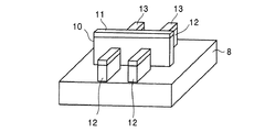
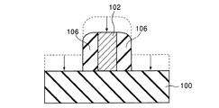
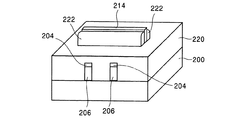
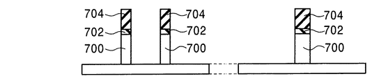
凸形状の突部が2種類以上ある半導体装置において、そのうちの一部の突部の側面だけに側壁材を存置させて、側壁部を形成したい場合もある。図1に示すFinFETは、突部に側壁部を作り分けしたい半導体装置の一例を示している。 In a semiconductor device having two or more types of projecting protrusions, it may be desired to form the sidewall parts by leaving the sidewall material only on the side surfaces of some of the protrusions. The FinFET shown in FIG. 1 is an example of a semiconductor device in which a side wall portion is desired to be formed on a protrusion.
この図1に示す半導体装置は、BOX(Buried Oxide)から形成された埋め込み絶縁膜8上に、第2の突部としてゲート電極10が設けられており、第1の突部としてソース/ドレインとなるFin12が設けられている。ゲート電極10の上側には、SiNハードマスク11が設けられており、Fin12の上側には、SiNハードマスク13が設けられている。
In the semiconductor device shown in FIG. 1, a
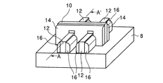
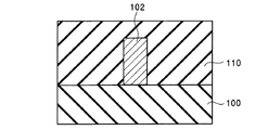
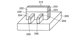
しかし、側壁残し工程で側壁部を構成する場合、突部のすべてに側壁部が形成されてしまう問題があった。すなわち、図1に示した半導体装置においては、図2に示すように、ゲート電極10の側壁部分には、側壁部14を形成する必要がある。しかし、このゲート電極10に側壁部14を形成すると、Fin12にも側壁部16が不可避的に形成されてしまう。
However, when the side wall portion is formed in the side wall leaving step, there is a problem that the side wall portion is formed on all of the protrusions. That is, in the semiconductor device shown in FIG. 1, as shown in FIG. 2, it is necessary to form the
このようにFin12に側壁部16が形成されてしまうと、Fin12にソース領域/ドレイン領域を形成するためにFin12にイオン打ち込みを行う際に、Fin12の側壁からイオン打ち込みができない。このため、Fin12の上方からイオン打ち込みを行っていた。
If the
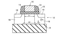
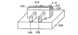
図3は、図2におけるA−A’線断面を示す図である。この図3に示すように、Fin12に上方からイオン打ち込みを行うと、Fin12の深さ方向に均一なソース領域/ドレイン領域18を形成できなくなってしまう。深さ方向に均一なソース/ドレイン領域18が形成できないと、Fin12上部におけるソース領域とドレイン領域との間の距離L1と、Fin12下部におけるソース領域とドレイン領域との間の距離L2とが、異なってしまう。また、Fin12下部のソース/ドレイン領域18に、高い寄生抵抗Rが発生してしまう。このため、トランジスタの駆動能力が劣化してしまうという問題が生じていた。
FIG. 3 is a diagram showing a cross section taken along line A-A ′ in FIG. 2. As shown in FIG. 3, if ion implantation is performed on
しかし側壁部14を形成しないと、Fin12にソース/ドレイン領域18を形成するためにイオン打ち込みを行った後、熱拡散を施すと、ソース/ドレイン領域18が互いに結合してしまう問題が生じる。また、側壁部14を形成しないと、ソース/ドレイン領域18の上部にシリサイド19を形成する際に、ソース/ドレイン領域18に形成したシリサイド19と、ゲート電極10に形成されたシリサイドとが、結合してしまうという問題も生じる。
However, if the
また、側壁残し工程で形成した側壁部を、エッチングパターンとして用いることにより、フォトリソグラフィーの限界よりも微細なパターンを形成する技術が知られている。このようなプロセスは、サイドウオールパターントランスファープロセス(Sidewall Pattern Transfer Process)と呼ばれており、例えば非特許文献1に開示されている。
本発明は、前記課題に鑑みてなされたものであり、高い駆動能力を有する半導体装置及びその製造方法を提供することを目的とする。また、サイドウオールパターントランスファーとフォトリソグラフィーを用いて微細なパターンと大きめのパターンを同時に形成できるようにすることを目的とする。 The present invention has been made in view of the above problems, and an object thereof is to provide a semiconductor device having a high driving capability and a method for manufacturing the same. It is another object of the present invention to form a fine pattern and a large pattern at the same time using sidewall pattern transfer and photolithography.
上記課題を解決するため、本発明に係る半導体装置の製造方法は、
凸状の第1の突部を形成する工程と、
前記第1の突部より高い位置に表面が位置するように、第1の膜を形成する工程と、
前記第1の膜上に、マスク部を形成する工程と、
前記マスク部をマスクとして用いて、前記第1の膜をエッチングする工程と、
を備えることを特徴とする。
In order to solve the above problems, a method of manufacturing a semiconductor device according to the present invention includes
Forming a convex first protrusion;
Forming a first film such that the surface is positioned higher than the first protrusion;
Forming a mask portion on the first film;
Etching the first film using the mask portion as a mask;
It is characterized by providing.
本発明に係る半導体装置は、
一方側にソース領域が形成され、他方側にドレイン領域が形成された、凸状半導体部と、
前記ソース領域と前記ドレイン領域との間における前記凸状半導体部上に、ゲート絶縁膜を介して形成されたゲート電極と、
前記ゲート電極の側壁部分の下側に形成された下側側壁部と、
前記ゲート電極の側壁部分における前記下側側壁部上に形成された上側側壁部であって、前記下側側壁部を構成する部材と異なる部材で構成された、上側側壁部と、
を有することを特徴とする。
A semiconductor device according to the present invention includes:
A convex semiconductor portion having a source region formed on one side and a drain region formed on the other side;
A gate electrode formed on the convex semiconductor portion between the source region and the drain region via a gate insulating film;
A lower side wall portion formed below the side wall portion of the gate electrode;
An upper side wall portion formed on the lower side wall portion in the side wall portion of the gate electrode, the upper side wall portion comprising a member different from the member constituting the lower side wall portion;
It is characterized by having.
本発明によれば、高い駆動能力を有する半導体装置及びその製造方法を提供することができる。また、サイドウオールパターントランスファーとフォトリソグラフィーを用いて微細なパターンと大きめのパターンを同時に形成することができる。 ADVANTAGE OF THE INVENTION According to this invention, the semiconductor device which has high drive capability, and its manufacturing method can be provided. Further, a fine pattern and a large pattern can be simultaneously formed by using side wall pattern transfer and photolithography.
〔第1実施形態〕
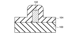
まず、本発明の基本概念を第1実施形態を例に説明する。図4に示すように、埋め込み絶縁膜100上に、凸形状の突部102を形成する。この突部102は本実施形態におけるデバイス構成要素である。続いて、この上に突部102の高さより薄い膜厚で、一定の厚さの膜104を形成する。但し、膜104は、必ずしも突部102の高さより薄い膜厚である必要はない。そして、全面異方性エッチングを行い、膜104の厚さ分だけエッチングする。すると、図5に示すように、突部102の側壁部分に膜104の材料が残留し、側壁部106が形成される。
[First Embodiment]
First, the basic concept of the present invention will be described using the first embodiment as an example. As shown in FIG. 4, a
これに対して、図6に示すように、突部102が形成された埋め込み絶縁膜100上に、突部102の高さより厚い膜厚で膜110を形成する。すなわち、膜110の表面が突部102よりも高い位置になるように、膜110を形成する。その後、膜110を平坦化する。そして、全面異方性エッチングを行い、絶縁膜100上の膜110の厚さ分だけエッチングする。すると、図7に示すように、突部102の側壁部分に膜110が残留せず、側壁部が形成されない。本実施形態では、この性質を応用する。
On the other hand, as shown in FIG. 6, a
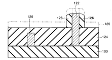
図8及び図9は、本実施形態に係る半導体装置の製造方法を説明する工程断面図である。図8に示すように、埋め込み絶縁膜100上に、第1の突部120と第2の突部122とを形成する。但し、第2の突部122の方が、第1の突部120よりも高くなるように形成する。これら第1の突部120と第2の突部122は、本実施形態におけるデバイス構成要素の一例である。
8 and 9 are process cross-sectional views illustrating the method for manufacturing the semiconductor device according to this embodiment. As shown in FIG. 8, a
次に、この上に、第1の膜124を全面的に形成し、平坦化及びエッチバックする。但し、エッチバック後の第1の膜124の厚さが、第1の突部120の高さより厚く、且つ、第2の突部122の高さより薄くなるようにする。換言すれば、第1の膜124の表面が、第1の突部120よりも高い位置で、且つ、第2の突部122よりも低い位置になるようにする。したがって、第1の突部120の頂部は第1の膜124から突出しないが、第2の突部122の頂部は第1の膜124の表面から突出する。
Next, a
次に、第2の膜125を全体的に形成し、全面異方性エッチングを行うことにより、第2の突部122の側壁部分に残留した第2の膜125で、第1の側壁部126を形成する。この全面異方性エッチングの際に、第1の膜124はエッチングされないようにするために、第2の膜125の材料は第1の膜の材料に対して、エッチング選択比の高いものを選定することが望ましい。この第1の側壁部126が本実施形態におけるマスク部に相当する。
Next, the
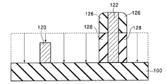
次に、図9に示すように、第1の側壁部126をマスクとして用いて、第1の膜124を異方性エッチングする。これにより、第2の突部122の側面部分に、第1の膜124が残留して、第2の側壁部128が形成される。但し、第1の突部120の側壁部分には、第1の膜124は残留せず、側壁部は形成されない。
Next, as shown in FIG. 9, the
以上のように、本実施形態に係る半導体装置の製造方法によれば、高い突部122の側面部分にだけ、側壁部126、128が形成され、低い方の突部120の側面部分には側壁部は形成されない。したがって、デバイス構成要素である突部が2種類以上ある半導体装置において、特定の突部の側面部分にのみ、側壁部を形成することができるようになる。すなわち、特定の突部の側面部分だけ側壁部で覆い、保護することが可能になる。
As described above, according to the manufacturing method of the semiconductor device according to the present embodiment, the
このことは、特定の突部以外の突部の側面を露出させ、その後の工程で、様々な加工処理を施すことができるようになることを意味する。 This means that the side surfaces of the protrusions other than the specific protrusions are exposed, and various processing processes can be performed in the subsequent steps.
〔第2実施形態〕
第2実施形態は、上述した第1実施形態を凸状半導体部の一例であるFinFETに適用したものである。より詳しくを、以下に説明する。
[Second Embodiment]
In the second embodiment, the above-described first embodiment is applied to a FinFET that is an example of a convex semiconductor portion. More details will be described below.
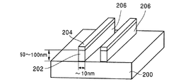
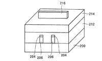
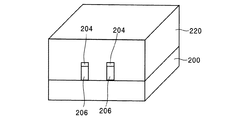
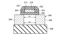
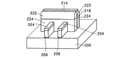
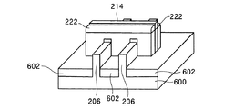
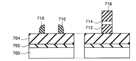
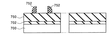
図10乃至図20は、本実施形態に係る半導体装置の製造工程を説明する断面図である。図10に示すように、SOI厚が50nm〜100nm程度のSOI基板を用意する。本実施形態では、半導体基板上に埋め込み絶縁膜200として、BOX(Buried Oxide)を用い、その上に50nm〜100nmのシリコン膜202を形成したSOI基板を用意する。続いて、70nm程度のSiNハードマスク204を形成し、パターニング、RIEを施すことにより、2つのFin206を形成する。本実施形態においては、このFin206の幅は10nm程度である。
10 to 20 are cross-sectional views illustrating the manufacturing process of the semiconductor device according to this embodiment. As shown in FIG. 10, an SOI substrate having an SOI thickness of about 50 nm to 100 nm is prepared. In this embodiment, an SOI substrate is prepared by using BOX (Buried Oxide) as a buried insulating
次に、図11に示すように、Fin206の側面にゲート絶縁膜(図示省略)を形成した後、第1層目のゲートポリシリコン208を形成する。本実施形態では、このゲートポリシリコン208は、300nm程度の膜厚で形成する。このゲートポリシリコン208は、Fin206の段差上に形成するため、その表面には大きな段差が形成される。
Next, as shown in FIG. 11, after forming a gate insulating film (not shown) on the side surface of the
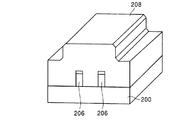
次に、図12に示すように、ゲートポリシリコン208をCMP(Chemical Mechanical Polishing)で平坦化し、SiNハードマスク204が露出するまでエッチバックする。続いて、図13に示すように、第2層目のゲートポリシリコン210を形成する。本実施形態では、このゲートポリシリコン210は、50nm程度の膜厚で形成する。ここでは、これらゲートポリシリコン208とゲートポリシリコン210とを合わせて、ゲートポリシリコン212とする。
Next, as shown in FIG. 12, the
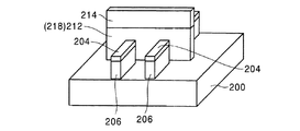
次に、図14に示すように、ゲートポリシリコン212上に、SiNハードマスク214を形成する。本実施形態においては、このSiNハードマスク214は、100nm程度の膜厚で形成する。続いて、このSiNハードマスク214上に、レジストを塗布してパターニングすることにより、ゲートパターン216を形成する。
Next, as shown in FIG. 14, a SiN
次に、図15に示すように、ゲートパターン216をマスクとして、RIEにより、SiNハードマスク214をエッチングした後、ゲートパターン216を除去する。続いて、このSiNハードマスク214をマスクにして、ゲートポリシリコン212とをエッチングする。これにより、ゲートポリシリコン212からゲート電極218が形成される。
Next, as shown in FIG. 15, after the SiN
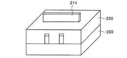
次に、図16に示すように、ゲート電極の側壁部分に側壁部を形成する材料(例えば、TEOS)で構成された絶縁膜220を、ゲート電極218の高さより高く全面的に形成し、平坦化する。続いて、図17に示すように、絶縁膜220をエッチバックし、ゲート電極218上のSiNハードマスク214を露出させる。
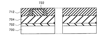
Next, as shown in FIG. 16, an insulating
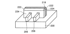
次に、図18に示すように、絶縁膜(例えば、SiN)を形成し、これをエッチバックすることにより、第1の側壁部222を形成する。なお、実際にはSiNハードマスク214の周囲全体に第1の側壁部222が形成されるが、この図18以下では分かりやすくするためSiNハードマスク214短辺方向に形成される第1の側壁部222は省いて図示している。
Next, as shown in FIG. 18, an insulating film (for example, SiN) is formed, and this is etched back to form the first
次に、図19に示すように、第1の側壁部222とSiNハードマスク214をマスクとして用いて、絶縁膜220をRIEでエッチングすることにより、ゲート電極218の側壁部分に残留した絶縁膜220により、第2の側壁部224を形成する。このためには、絶縁膜220は、第1の側壁部222とSiNハードマスク214とに対して高いエッチング選択比を有していることが望ましい。
Next, as shown in FIG. 19, the insulating
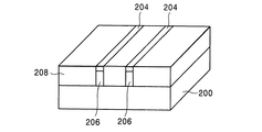
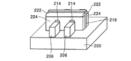
次に、図20に示すように、SiN−RIEを行うことにより、Fin206上のSiNハードマスク204をエッチングにより除去する。続いて、Fin206の側面にドーピングを行って、ソース/ドレイン領域を形成するとともに、形成したソース/ドレイン領域にシリサイド貼り付けを行う。Fin206側面へのドーピングは、斜めからのイオン注入で行うこともできるし、プラズマドーピングや固層拡散により行うこともできる。また、シリサイド材料としては、例えば、NiSiを用いることができる。
Next, as shown in FIG. 20, by performing SiN-RIE, the SiN
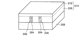
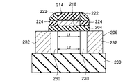
図21は、シリサイド後の図20におけるB―B’線断面図である。この図21に示すように、第1の側壁部222及び第2の側壁部224はゲート電極218の側壁部分にだけ形成され、Fin206の側壁分には形成されない。このため、Fin206に側面からドーピングをして、Fin206の一方側にソース拡散層領域230を形成し、Fin206の他方側にドレイン拡散層領域230を形成することができるとともに、側面にシリサイド232を貼り付けることができる。
21 is a cross-sectional view taken along line B-B ′ in FIG. 20 after silicidation. As shown in FIG. 21, the
側面からドーピングをすると、Fin206上部のソース領域とドレイン領域との間の距離L1と、Fin206下部のソース領域とドレイン領域との間の距離L2とが実質的に等しくなり、Fin206の深さ方向に均一なソース/ドレイン領域230を形成することができる。つまり、実効チャネル長を、Fin206の深さ方向に均一にすることができる。また、Fin206の下部にまで十分なドーピングとシリサイド形成を行うことができるので、寄生抵抗Rを低減することができ、トランジスタの駆動能力の向上を図ることができる。
When doping is performed from the side surface, the distance L1 between the source region and the drain region above the
〔第3実施形態〕
図22は、第3実施形態に係る半導体装置を説明する断面図であり、上述した第2実施形態における図21に対応する図である。上述した第2実施形態と異なる部分だけ説明すると、図22に示すように、本実施形態においては、ソース/ドレイン領域には不純物拡散層を形成せずに、シリサイド300のみを貼り付ける。すなわち、ショットキー接合ソース/ドレイン構造のFinFETを形成する。それ以外の製造工程及び構造は上述した第2実施形態と同様である。
[Third Embodiment]
FIG. 22 is a cross-sectional view illustrating the semiconductor device according to the third embodiment, and corresponds to FIG. 21 in the second embodiment described above. Explaining only the differences from the second embodiment described above, as shown in FIG. 22, in this embodiment, only the
本実施形態によれば、ゲート電極218の側面部分には第1の側壁部222及び第2の側壁部224が形成されるが、Fin206の側面部分には側壁部が形成されない。このため、Fin206の側壁面にシリサイド300を貼り付けることが可能になる。これにより、Fin206の深さ方向に対して均一なショットキーソース/ドレイン領域を形成できる。すなわち、Fin206上部におけるショットキーソース領域とショットキードレイン領域との間の距離L1と、Fin206下部におけるショットキーソース領域とショットキードレイン領域との間の距離L2とを、実質的に等しくすることができる。つまり、実効チャネル長をFin206の深さ方向に均一にすることができる。
According to the present embodiment, the first
また、ショットキーソース/ドレイン領域の下部に低抵抗なシリサイド300が形成されるため、寄生抵抗Rが低減され、トランジスタの駆動能力を向上させることができる。
Further, since the low-
なお、ショットキーコンタクト抵抗を低減するため、シリサイド300の材料としてはショットキーバリアの小さい材料を用いることが望ましい。例えば、n型のMOSトランジスタの場合には、バンドギャップの中央値よりも仕事関数の小さいEr等をシリサイド300の材料に用いて、ErSiによりシリサイド300を構成すればよい。p型のMOSトランジスタの場合には、バンドギャップの中央値よりも仕事関数の大きいPt等をシリサイド300の材料に用いて、PtSiによりシリサイド300を構成すればよい。
In order to reduce the Schottky contact resistance, it is desirable to use a material having a small Schottky barrier as the material of the
〔第4実施形態〕
図23は、第4実施形態に係る半導体装置を説明する断面図である。この図23に示すように、本実施形態においても、上述した第2実施形態と同様に、ゲート電極218の側面部分には第1の側壁部222及び第2の側壁部224を形成しているが、Fin206の側面部分には側壁部を形成していない。
[Fourth Embodiment]
FIG. 23 is a cross-sectional view illustrating a semiconductor device according to the fourth embodiment. As shown in FIG. 23, also in the present embodiment, the first
但し、本実施形態においては、ソース/ドレイン領域として不純物拡散層を形成した後、例えば、エピタキシャル成長により、ソース/ドレイン部分を持ち上げる。すなわち、Fin206の上面及び側面が露出しているので、Fin206の上面及び側面にエピタキシャル成長によりエピタキシャルシリコン部400を形成することができる。このエピタキシャルシリコン部400を形成した後、必要に応じて、さらに不純物イオン注入やシリサイド形成を行ってもよい。
However, in the present embodiment, after the impurity diffusion layer is formed as the source / drain region, the source / drain portion is lifted, for example, by epitaxial growth. That is, since the upper surface and side surfaces of the
本実施形態に係る半導体装置の製造方法によれば、Fin206の側面部分には側壁部が形成されていないため、エピタキシャル成長により、エピタキシャルシリコン部400を形成することができる。そして、エピタキシャルシリコン部400を形成することにより、ソース/ドレイン領域の寄生抵抗Rが低減されるため、トランジスタの駆動能力を向上させることができる。
According to the method for manufacturing a semiconductor device according to the present embodiment, since the side wall portion is not formed on the side surface portion of
〔第5実施形態〕
図24乃至図26は、第5実施形態に係る半導体装置の製造工程を説明する断面図である。図24に至るまでは上述した第2実施形態と同様の製造工程である。すなわち、ゲート電極218の側面部分には、第1の側壁部222と第2の側壁部224が形成されているが、Fin206の側面部分には側壁部は形成されていない。
[Fifth Embodiment]
24 to 26 are cross-sectional views illustrating the manufacturing process of the semiconductor device according to the fifth embodiment. Up to FIG. 24, the manufacturing process is the same as that of the second embodiment described above. That is, the first
続いて、図25に示すように、SiN−RIEを行い、Fin206上のSiNハードマスク204とゲート電極218上のSiNハードマスク214とを除去する。続いて、ソース/ドレイン領域を形成するために、ドーピングによりFin206の左右両端側に不純物拡散層を形成する。
Subsequently, as shown in FIG. 25, SiN-RIE is performed to remove the SiN
次に、図26に示すように、Fin206のソース/ドレイン部分とゲート電極218をすべてシリサイド化して、それぞれ、メタルソース/ドレインとメタルゲート電極にする。ゲート電極218は、非常に薄く形成されており、且つ、その下部が埋め込み絶縁膜200になっており、この埋め込み絶縁膜200はそもそもシリサイド化しないため、本実施形態においては、ゲート電極218はその下端部までシリサイド化できる。
Next, as shown in FIG. 26, the source / drain portion of
本実施形態によれば、ゲート電極218の側面部分には、第1の側壁部222と第2の側壁部224が形成されるが、Fin206の側壁部分には側壁部は形成されないため、Fin206の側面にシリサイドを形成することができる。このため、ソース/ドレイン領域の寄生抵抗Rが低減され、トランジスタの駆動能力を向上させることができる。また、ゲート電極218を構成するポリシリコンをすべてシリサイド化して、メタルゲートを形成できるため、完全空乏化型トランジスタ(FinFET)のしきい値をコントロールでき、低電圧で高駆動力を実現することができる。
According to the present embodiment, the first
なお、本発明は上記実施形態に限定されず種々に変形可能である。例えば、図27に示すように、シリコン基板600上に、上述した各実施形態の製造工程により、FinFETを形成するようにしてもよい。この場合、シリコン基板600をエッチングすることにより、Fin206を形成し、Fin206の間にシリコン酸化膜602等からSTI(Shallow Trench Isolation)を形成すればよい。
In addition, this invention is not limited to the said embodiment, A various deformation | transformation is possible. For example, as shown in FIG. 27, a FinFET may be formed on a
また、上述した実施形態では、本発明を適用する半導体装置としてFinFETを例に説明したが、他の種類の半導体装置にも本発明を適用することができる。 In the above-described embodiments, the FinFET is described as an example of a semiconductor device to which the present invention is applied. However, the present invention can also be applied to other types of semiconductor devices.
〔第6実施形態〕
Fin(凸状シリコン領域、アクティブエリア)やゲート電極の形成に、サイドウオールパターントランスファープロセス(Sidewall Pattern Transfer Process)を用いると、フォトリソグラフィーの限界よりも微細で、且つ、ラインエッジラフネス(LER: Line Edge Roughness)の小さいパターンを形成することができる。以下、製造工程を順に説明する。
[Sixth Embodiment]
When the side wall pattern transfer process is used to form Fin (convex silicon region, active area) and gate electrode, the line edge roughness (LER: Line) is finer than the limit of photolithography. A pattern with a small edge roughness can be formed. Hereinafter, the manufacturing process will be described in order.
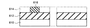
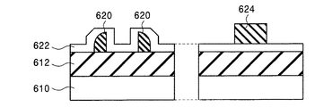
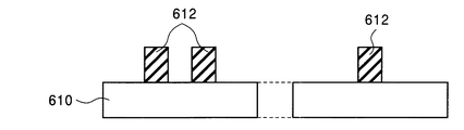
まず、図28に示すように、半導体基板610上に、図示していない薄い酸化膜を介してシリコン窒化膜612を形成する。本実施形態においては、このシリコン窒化膜612の厚さは、例えば、100nmである。続いて、このシリコン窒化膜612上に、アモルファスシリコン層614を例えば150nm程度の厚さで形成する。続いて、このアモルファスシリコン層614上に、フォトリソグラフィーを用いて幅0.1μm程度のレジストパターンを形成し、このレジストパターンをマスクとして用いて、アモルファスシリコン層614をRIEによりエッチングする。これにより、ダミーパターン616が得られる。
First, as shown in FIG. 28, a
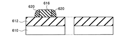
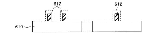
次に、図29に示すように、この上に、例えば厚さ40nm程度のTEOSを形成した後、全面RIEでエッチバックすることにより、ダミーパターン616の側面部分に、側壁部620を形成する。
Next, as shown in FIG. 29, a TEOS having a thickness of, for example, about 40 nm is formed thereon, and then etched back by the entire surface RIE, thereby forming a
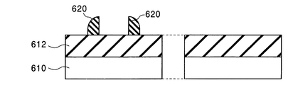
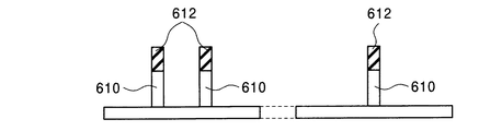
次に、図30に示すように、アモルファスシリコンにより形成されたダミーパターン616を、エッチングにより除去し、シリコン窒化膜612上に、TEOSから形成された側壁部620を残す。
Next, as shown in FIG. 30, the
次に、図31に示すように、この上に、光の反射を防止するための反射防止膜(ARC:Anti Reflective Coating)622を形成する。続いて、反射防止膜622上にフォトレジストを形成し、このフォトレジストをフォトリソグラフィーを用いてパターニングすることにより、レジストパターン624を形成する。本実施形態においては、このレジストパターン624の幅は、側壁部620の幅よりも、太く形成される。なお、上述した非特許文献1にも開示されているように、このレジストパターン624と、側壁部620は、互いに重なる部分があってもよい。
Next, as shown in FIG. 31, an antireflection film (ARC: Anti Reflective Coating) 622 for preventing reflection of light is formed thereon. Subsequently, a photoresist is formed on the
次に、図32に示すように、このレジストパターン624と側壁部620とをマスクとして用いて、シリコン窒化膜612をRIEによりエッチングする。続いて、側壁部620とレジストパターン624とを、ウエットエッチング等により除去する。
Next, as shown in FIG. 32, the
次に、図33に示すように、シリコン窒化膜612を、ホットリン酸などのウエットエッチングにより細らせる。次に、図34に示すように、半導体基板610をRIEにより加工する。
Next, as shown in FIG. 33, the
このようにすると、側壁部620のパターントランスファーにより、フォトリソグラフィーの限界よりも微細で、且つ、ラインエッジラフネス(LER)の小さい、パターンを形成することができる。LERが低減する理由は、側壁部620のパターンのライン幅が、TEOSを形成する厚さで定まるからである。
In this case, a pattern that is finer than the limit of photolithography and has a small line edge roughness (LER) can be formed by pattern transfer of the
しかしながら、図31及び図32から分かるように、レジストパターン624を反射防止膜622を用いて形成すると、反射防止膜622が側壁部620の側面に残留してしまい、せっかく作った細い側壁部620のラインパターンが太くなってしまうという問題が生じる。一方で、フォトリソグラフィーの際に、光が乱反射すると、レジストパターン624の形状が乱れてしまい、微細化の妨げになってしまう。このため、レジストパターン624の微細化を図る上では、反射防止膜622を省くことは困難である。
However, as can be seen from FIGS. 31 and 32, when the resist
〔第7実施形態〕
そこで、第7実施形態では、側壁部620のラインパターンが反射防止膜622により太くならないようにしている。
[Seventh Embodiment]
Therefore, in the seventh embodiment, the line pattern of the
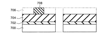
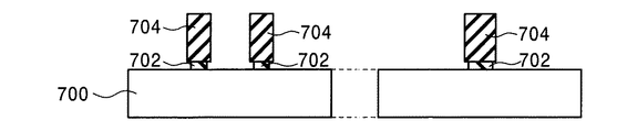
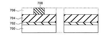
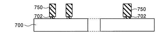
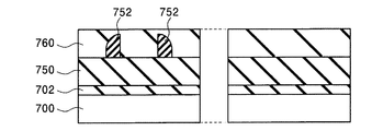
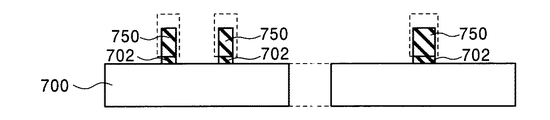
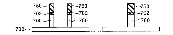
まず、図35に示すように、本実施形態においては、シリコンから構成された半導体基板700上に、絶縁膜702が形成されている。この絶縁膜は、例えば、シリコン酸化膜(SiO2)により構成されている。
First, as shown in FIG. 35, in this embodiment, an insulating
次に、この絶縁膜702上に、シリコン窒化膜704を形成する。本実施形態においては、このシリコン窒化膜704の厚さは、例えば、100nmである。なお、半導体基板700とシリコン窒化膜704との間に、シリコン酸化膜の絶縁膜702を形成するのは、シリコン酸化膜の絶縁膜702を介在させることにより、応力の緩和を図るためである。このシリコン窒化膜704が本実施形態における第2の膜に相当する。
Next, a
続いて、このシリコン窒化膜704上に、アモルファスシリコン層706を例えば150nm程度形成する。続いて、このアモルファスシリコン層706上に、フォトリソグラフィーを用いて幅0.1μm程度のレジストパターンを形成し、このレジストパターンをマスクとして用いて、アモルファスシリコン層706をRIEによりエッチングする。これにより、ダミーパターン708が得られる。
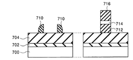
Subsequently, an
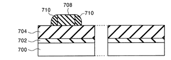
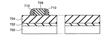
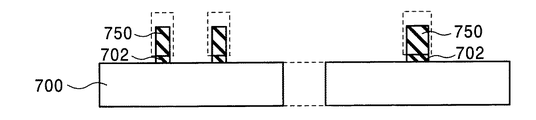
次に、図36に示すように、この上に、例えば厚さ40nm程度のTEOSを形成した後、全面RIEでエッチバックすることにより、ダミーパターン708の側面部分に、側壁部710を形成する。
Next, as shown in FIG. 36, for example, TEOS having a thickness of about 40 nm is formed thereon, and then etched back by the entire surface RIE, thereby forming a
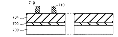
次に、図37に示すように、アモルファスシリコンにより形成されたダミーパターン708を、エッチングにより除去し、シリコン窒化膜704上に、TEOSから形成された側壁部710を残す。この側壁部710が本実施形態における第1の突部に相当する。
Next, as shown in FIG. 37, the
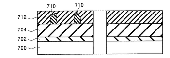
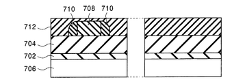
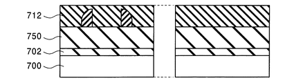
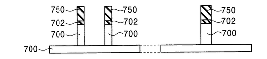
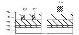
次に、図38に示すように、TEOSから形成されている側壁部710とは異なる材料(例えば、アモルファスシリコン)を堆積して、CMP(Chemical Mechanical Polishing)により平坦化することにより、下地膜712を形成する。この下地膜712が本実施形態における第1の膜に相当する。
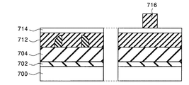
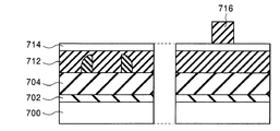
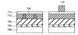
Next, as shown in FIG. 38, a
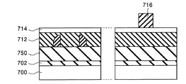
次に、図39に示すように、この下地膜712上に、光の反射を防止する反射防止膜(ARC:Anti Reflective Coating)714を形成する。続いて、反射防止膜714上にフォトレジストを形成し、このフォトレジストをフォトリソグラフィーでパターニングすることにより、レジストパターン716を形成する。本実施形態においては、このレジストパターン716の幅は、側壁部710の幅よりも、太く形成される。このレジストパターン716が本実施形態におけるマスク部に相当する。
Next, as shown in FIG. 39, an antireflection film (ARC) 714 for preventing light reflection is formed on the
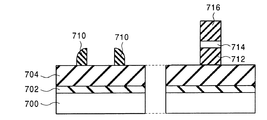
次に、図40に示すように、このレジストパターン716をマスクとして用いて、下地膜712をRIEによりエッチングする。このとき、先ほど形成しておいた側壁部710が露出する。そして、レジストパターン716を除去する。
Next, as shown in FIG. 40, the
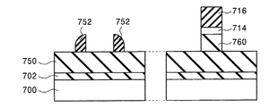
次に、図41に示すように、側壁部710と下地膜712の双方をマスクとして用いて、シリコン窒化膜704をRIEによりエッチングする。続いて、側壁部710と下地膜712とを、ウエットエッチング等により除去する。TEOSの側壁部710をHF等のウエットエッチングで除去するとき、絶縁膜702もエッチングされる。
Next, as shown in FIG. 41, the
次に、図42に示すように、シリコン窒化膜704を、ホットリン酸などのウエットエッチングにより細らせる。次に、図43に示すように、半導体基板700をRIEにより加工する。
Next, as shown in FIG. 42, the
以上のように、本実施形態によれば、TEOSにより形成された側壁部710のパターントランスファーにより、フォトリソグラフィーの限界以下の微細加工を施すことができ、且つ、ラインエッジラフネス(LER: line edge roughness)の小さいシリコンパターンを形成することができる。
As described above, according to the present embodiment, fine processing below the limit of photolithography can be performed by pattern transfer of the
また、反射防止膜714を用いて、フォトリソグラフィーによるレジストパターン716を形成した場合でも、反射防止膜714が側壁部710の側面に残留しないので、側壁部710のパターン幅が太くなってしまうのを回避することができる。
Further, even when the resist
〔第8実施形態〕
本実施形態は、側壁部710を形成した後に、アモルファスシリコンのダミーパターン708を除去せずに、2回目のアモルファスシリコンを重ねて形成する点で、上述した第7実施形態と相違する。以下、製造工程を順に説明する。
[Eighth Embodiment]
The present embodiment is different from the above-described seventh embodiment in that the amorphous
図44に示すように、本実施形態においては、シリコンから構成された半導体基板700上に、絶縁膜702が形成されている。この絶縁膜は、例えば、シリコン酸化膜(SiO2)により構成されている。
As shown in FIG. 44, in this embodiment, an insulating
次に、この絶縁膜702上に、シリコン窒化膜704を形成する。本実施形態においては、このシリコン窒化膜704の厚さは、例えば、100nmである。続いて、このシリコン窒化膜704上に、アモルファスシリコン層706を例えば150nm程度形成する。続いて、このアモルファスシリコン層706上に、フォトリソグラフィーを用いて幅0.1μm程度のレジストパターンを形成し、このレジストパターンをマスクとして用いて、アモルファスシリコン層706をRIEによりエッチングする。これにより、ダミーパターン708が得られる。
Next, a
次に、図45に示すように、この上に、例えば厚さ40nm程度のTEOSを形成した後、全面RIEでエッチバックすることにより、ダミーパターン708の側面部分に、側壁部710を形成する。
Next, as shown in FIG. 45, a TEOS having a thickness of, for example, about 40 nm is formed thereon, and then etched back by the entire surface RIE, thereby forming a
次に、図46に示すように、これら側壁部710とダミーパターン708との上に、TEOSから形成されている側壁部710とは異なる材料(例えば、アモルファスシリコン)を堆積して、CMPにより平坦化することにより、下地膜712を形成する。
Next, as shown in FIG. 46, a material (for example, amorphous silicon) different from the
次に、図47に示すように、この下地膜712上に、光の反射を防止する反射防止膜(ARC:Anti Reflective Coating)714を形成する。続いて、反射防止膜714上にフォトレジストを形成し、このフォトレジストをフォトリソグラフィーでパターニングすることにより、レジストパターン716を形成する。本実施形態においては、このレジストパターン716の幅は、側壁部710の幅よりも、太く形成される。
Next, as shown in FIG. 47, an antireflection film (ARC) 714 for preventing light reflection is formed on the
次に、図48に示すように、このレジストパターン716をマスクとして用いて、下地膜712をRIEによりエッチングする。このエッチングにより、ダミーパターン708も合わせて除去され、先ほど形成しておいた側壁部710が露出する。以下の製造工程は、上述した第7実施形態と同様であるので、説明は省略する。
Next, as shown in FIG. 48, the
以上のように、本実施形態においても、TEOSにより形成された側壁部710のパターントランスファーにより、フォトリソグラフィーの限界以下の微細加工を施すことができ、且つ、ラインエッジラフネス(LER: line edge roughness)の小さいシリコンパターンを形成することができる。
As described above, also in this embodiment, fine processing below the limit of photolithography can be performed by pattern transfer of the
また、側壁部710の間に位置するダミーパターン708を、下地膜712とともに、1回のRIEで除去することとしたので、製造プロセスにおける工程数を削減することができ、コスト低減を図ることができる。
In addition, since the
〔第9実施形態〕
本実施形態は、アモルファスシリコンのダミーパターン708の表面に、ポリッシングの際のストッパー部を形成する点で、上述した第8実施形態と相違する。以下、製造工程を順に説明する。
[Ninth Embodiment]
This embodiment is different from the above-described eighth embodiment in that a stopper portion for polishing is formed on the surface of the amorphous
図49に示すように、本実施形態においては、シリコンから構成された半導体基板700上に、絶縁膜702が形成されている。この絶縁膜は、例えば、シリコン酸化膜(SiO2)により構成されている。
As shown in FIG. 49, in this embodiment, an insulating
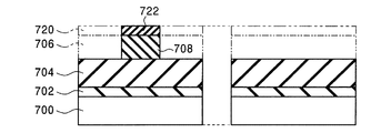
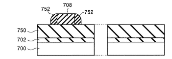
次に、この絶縁膜702上に、シリコン窒化膜704を形成する。本実施形態においては、このシリコン窒化膜704の厚さは、例えば、100nmである。続いて、このシリコン窒化膜704上に、アモルファスシリコン層706を例えば150nm程度形成する。続いて、このアモルファスシリコン層706上に、シリコン窒化膜720を形成する。本実施形態においては、このシリコン窒化膜720は、例えば、50nm程度形成する。
Next, a
次に、このシリコン窒化膜720上に、フォトリソグラフィーを用いて幅0.1μm程度のレジストパターンを形成し、このレジストパターンをマスクとして用いて、シリコン窒化膜720とアモルファスシリコン層706をRIEによりエッチングする。これにより、シリコン窒化膜720からストッパー部722が得られ、アモルファスシリコン層706からダミーパターン708が得られる。
Next, a resist pattern having a width of about 0.1 μm is formed on the
次に、図50に示すように、この上に、例えば厚さ40nm程度のTEOSを形成した後、全面RIEでエッチバックを行うことにより、ダミーパターン708の側面部分に、側壁部710を形成する。
Next, as shown in FIG. 50, a TEOS having a thickness of, for example, about 40 nm is formed thereon, and then etched back by the entire surface RIE, thereby forming a
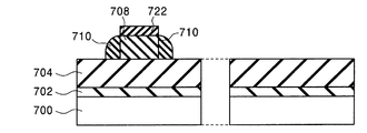
次に、図51に示すように、これら側壁部710とダミーパターン708との上に、TEOSから形成されている側壁部710とは異なる材料(例えば、アモルファスシリコン)を堆積して、CMPにより平坦化することにより、下地膜712を形成する。このCMPを行う際に、ストッパー部722がストッパーとしてはたらく。但し、CMPで薄くなったシリコン窒化膜720の膜厚が、20nm程度以下となるように、プロセスを調整しておくことが望ましい。
Next, as shown in FIG. 51, a material (for example, amorphous silicon) different from the
次に、図52に示すように、CMPで薄くなったストッパー部722を除去し、下地膜712上に、光の反射を防止する反射防止膜(ARC:Anti Reflective Coating)714を形成する。続いて、反射防止膜714上にフォトレジストを形成し、このフォトレジストをフォトリソグラフィーでパターニングすることにより、レジストパターン716を形成する。本実施形態においては、このレジストパターン716の幅は、側壁部710の幅よりも、太く形成される。
Next, as shown in FIG. 52, the
次に、図53に示すように、このレジストパターン716をマスクとして用いて、下地膜712をRIEによりエッチングする。このエッチングにより、ダミーパターン708も合わせて除去され、先ほど形成しておいた側壁部710が露出する。以下の製造工程は、上述した第7実施形態と同様であるので、説明は省略する。
Next, as shown in FIG. 53, the
以上のように、本実施形態においても、TEOSにより形成された側壁部710のパターントランスファーにより、フォトリソグラフィーの限界以下の微細加工を施すことができ、且つ、ラインエッジラフネス(LER: line edge roughness)の小さいシリコンパターンを形成することができる。
As described above, also in the present embodiment, fine processing below the limit of photolithography can be performed by pattern transfer of the
また、下地膜712をポリッシング(本実施形態では、CMP)で平坦化する際に、ストッパー部722がストッパとして機能するので、ポリッシングが行いやすくなる。
In addition, when the
〔第10実施形態〕
本実施形態は、上述した第7実施形態におけるシリコン加工用のハードマスク704の形成材料と、側壁部710の形成材料とを入れ替えたものである。以下、製造工程を順に説明する。
[Tenth embodiment]
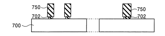
In the present embodiment, the material for forming the
図54に示すように、本実施形態においては、シリコンから構成された半導体基板700上に、絶縁膜702が形成されている。この絶縁膜は、例えば、シリコン酸化膜(SiO2)により構成されている。
As shown in FIG. 54, in this embodiment, an insulating
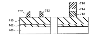
次に、この絶縁膜702上に、TEOS膜750を形成する。本実施形態においては、このTEOS膜750の厚さは、例えば、100nmである。続いて、このTEOS膜750上に、アモルファスシリコン層706を例えば150nm程度形成する。続いて、このアモルファスシリコン層706上に、フォトリソグラフィーを用いて幅0.1μm程度のレジストパターンを形成し、このレジストパターンをマスクとして用いて、アモルファスシリコン層706をRIEによりエッチングする。これにより、ダミーパターン708が得られる。
Next, a
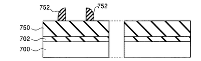
次に、図55に示すように、この上に、例えば厚さ40nm程度のシリコン窒化膜を形成した後、全面RIEによりエッチバックを行うことにより、ダミーパターン708の側面部分に、側壁部752を形成する。
Next, as shown in FIG. 55, a silicon nitride film having a thickness of, for example, about 40 nm is formed thereon, and then etched back by RIE on the entire surface, so that the
次に、図56に示すように、アモルファスシリコンにより形成されたダミーパターン708を、エッチングにより除去し、TEOS膜750上に、窒化シリコンから形成された側壁部752を残す。
Next, as shown in FIG. 56, the
次に、図57に示すように、窒化シリコンから形成されている側壁部752とは異なる材料(例えば、アモルファスシリコン)を堆積して、CMPにより平坦化することにより、下地膜712を形成する。
Next, as shown in FIG. 57, a
次に、図58に示すように、この下地膜712上に、光の反射を防止する反射防止膜(ARC:Anti Reflective Coating)714を形成する。続いて、反射防止膜714上にフォトレジストを形成し、このフォトレジストをフォトリソグラフィーでパターニングすることにより、レジストパターン716を形成する。本実施形態においては、このレジストパターン716の幅は、側壁部710の幅よりも、太く形成される。
Next, as shown in FIG. 58, an antireflection film (ARC) 714 for preventing light reflection is formed on the
次に、図59に示すように、このレジストパターン716をマスクとして用いて、下地膜712をRIEによりエッチングする。このとき、先ほど形成しておいた側壁部752が露出する。そして、レジストパターン716を除去する。
Next, as shown in FIG. 59, the
次に、図60に示すように、側壁部752と下地膜712の双方をマスクとして用いて、TEOS膜750をRIEによりエッチングする。続いて、側壁部752と下地膜712とを、ウエットエッチング等により除去する。
Next, as shown in FIG. 60, the
次に、図61に示すように、TEOS膜750を、HFなどのウエットエッチングにより細らせる。次に、図62に示すように、半導体基板700をRIEにより加工する。
Next, as shown in FIG. 61, the
このように、本発明の材料の組み合わせは、種々に選択可能である。すなわち、エッチングの際の選択比を確保しながら、種々の材料を組み合わせることができる。また、第9実施形態のように、ストッパー部722を形成する場合でも、このストッパー部722を含めて、種々の材料を組み合わせを選択することができる。
Thus, various combinations of the materials of the present invention can be selected. That is, various materials can be combined while securing the selection ratio during etching. Further, even when the
〔第11実施形態〕
本実施形態は、上述した第10実施形態において、アモルファスシリコンで形成した下地膜712を、SOG膜(塗布膜)で形成するようにしたものである。以下、製造工程を順に説明する。
[Eleventh embodiment]
In the present embodiment, the
本実施形態においては、図63に至るまでの製造工程は、上述した第10実施形態と同様である。この図63に続いて、本実施形態においては、図64に示すように、窒化シリコンから形成されている側壁部752とは異なる材料であるSOGを塗布する。SOGを塗布することにより、SOGの表面は平坦化するので、これを下地膜760とする。
In the present embodiment, the manufacturing process up to FIG. 63 is the same as that in the tenth embodiment described above. Subsequent to FIG. 63, in this embodiment, as shown in FIG. 64, SOG which is a material different from the
次に、図65に示すように、この下地膜760上に、光の反射を防止する反射防止膜(ARC:Anti Reflective Coating)714を形成する。続いて、反射防止膜714上にフォトレジストを形成し、このフォトレジストをフォトリソグラフィーでパターニングすることにより、レジストパターン716を形成する。本実施形態においては、このレジストパターン716の幅は、側壁部752の幅よりも、太く形成される。
Next, as shown in FIG. 65, an antireflection film (ARC: Anti Reflective Coating) 714 for preventing light reflection is formed on the
次に、図66に示すように、このレジストパターン716をマスクとして用いて、下地膜760をRIEによりエッチングする。このとき、先ほど形成しておいた側壁部752が露出する。
Next, as shown in FIG. 66, the
次に、図67に示すように、側壁部752と下地膜760及びレジストパターン716の双方をマスクとして用いて、TEOS膜750をRIEによりエッチングする。続いて、側壁部752と下地膜760とレジストパターン716を、ウエットエッチング等により除去する。
Next, as shown in FIG. 67, the
次に、図68に示すように、TEOS膜750を、HFなどのウエットエッチングにより細らせる。次に、図69に示すように、半導体基板700をRIEにより加工する。
Next, as shown in FIG. 68, the
以上のように、本実施形態においても、SiNにより形成された側壁部752のパターントランスファーにより、フォトリソグラフィーの限界以下の微細加工を施すことができ、且つ、ラインエッジラフネス(LER: line edge roughness)の小さいシリコンパターンを形成することができる。
As described above, also in the present embodiment, fine processing below the limit of photolithography can be performed by pattern transfer of the
また、液体であるSOGを塗布することにより、下地膜760を形成することとしたので、表面を平坦化するためのポリッシング工程を省略することができる。
In addition, since the
なお、本発明は上記実施形態に限定されず、種々に変形可能である。例えば、上述した実施形態では、シリコンで構成された半導体基板700を使用したが、ゲルマニウム基板や、シリコンゲルマニウム基板を半導体基板として用いるようにしてもよい。
In addition, this invention is not limited to the said embodiment, A various deformation | transformation is possible. For example, in the embodiment described above, the
100 埋め込み絶縁膜
120 第1の突部
122 第2の突部
124 第1の膜
125 第2の膜
126 第1の側壁部
128 第2の側壁部
700 半導体基板
702 絶縁膜
704 シリコン窒化膜
706 アモルファスシリコン層
708 ダミーパターン
710 側壁部
712 下地膜
714 反射防止膜
716 レジストパターン
100 buried insulating
Claims (7)
前記第1の突部より高い位置に表面が位置するように、第1の膜を形成する工程と、
前記第1の膜上に、マスク部を形成する工程と、
前記マスク部をマスクとして用いて、前記第1の膜をエッチングする工程と、
を備えることを特徴とする半導体装置の製造方法。 Forming a convex first protrusion;
Forming a first film such that the surface is positioned higher than the first protrusion;
Forming a mask portion on the first film;
Etching the first film using the mask portion as a mask;
A method for manufacturing a semiconductor device, comprising:
前記第1の膜を形成する工程では、前記第1の突部より高く、且つ、前記第2の突部より低い位置に、表面が位置するように前記第1の膜が形成される、ことを特徴とする請求項1に記載の半導体装置の製造方法。 Further comprising a step of forming a convex second protrusion that is higher than the first protrusion,
In the step of forming the first film, the first film is formed so that the surface is located at a position higher than the first protrusion and lower than the second protrusion. The method of manufacturing a semiconductor device according to claim 1.
前記第1の膜上及び前記第1の膜の表面から突出している前記第2の突部上に、第2の膜を形成する工程と、
前記第2の膜をエッチバックすることにより、前記第2の突部の側面に前記第2の膜を残留させて、これを前記マスク部とする工程と、
をさらに備えることを特徴とする請求項2に記載の半導体装置の製造方法。 The step of forming the mask portion includes:
Forming a second film on the first film and on the second protrusion protruding from the surface of the first film;
Etching back the second film to leave the second film on the side surface of the second protrusion, which is used as the mask part;
The method of manufacturing a semiconductor device according to claim 2, further comprising:
前記第1の突部を形成する工程は、
前記第2の膜上に、ダミーパターンを形成する工程と、
前記第2の膜上、及び、前記ダミーパターン上に、第3の膜を形成する工程と、
前記第3の膜をエッチバックすることにより、前記ダミーパターンの側面に前記第3の膜を残留させて、これを前記第1の突部とする工程と、
を備える、ことを特徴とする請求項1に記載の半導体基板の製造方法。 And further comprising forming a second film on the semiconductor substrate,
The step of forming the first protrusion includes
Forming a dummy pattern on the second film;
Forming a third film on the second film and on the dummy pattern;
Etching back the third film to leave the third film on the side surface of the dummy pattern, which is used as the first protrusion;
The method for manufacturing a semiconductor substrate according to claim 1, comprising:
前記第1の膜上に、光の反射を防止する反射防止膜を形成する工程と、
前記反射防止膜上に、フォトレジストを形成する工程と、
前記フォトレジストを、フォトリソグラフィーによりパターニングすることにより、前記マスク部を形成する工程と、
を備えることを特徴とする請求項5に記載の半導体装置の製造方法。 The step of forming the mask portion includes:
Forming an antireflection film for preventing reflection of light on the first film;
Forming a photoresist on the antireflection film;
Forming the mask portion by patterning the photoresist by photolithography; and
The method of manufacturing a semiconductor device according to claim 5, comprising:
前記ソース領域と前記ドレイン領域との間における前記凸状半導体部上に、ゲート絶縁膜を介して形成されたゲート電極と、
前記ゲート電極の側壁部分の下側に形成された下側側壁部と、
前記ゲート電極の側壁部分における前記下側側壁部上に形成された上側側壁部であって、前記下側側壁部を構成する部材と異なる部材で構成された、上側側壁部と、
を有することを特徴とする半導体装置。 A convex semiconductor portion having a source region formed on one side and a drain region formed on the other side;
A gate electrode formed on the convex semiconductor portion between the source region and the drain region via a gate insulating film;
A lower side wall portion formed below the side wall portion of the gate electrode;
An upper side wall portion formed on the lower side wall portion in the side wall portion of the gate electrode, the upper side wall portion comprising a member different from the member constituting the lower side wall portion;
A semiconductor device comprising:
Priority Applications (2)
| Application Number | Priority Date | Filing Date | Title |
|---|---|---|---|
| JP2004150519A JP2005294789A (en) | 2004-03-10 | 2004-05-20 | Semiconductor device and manufacturing method thereof |
| US11/058,190 US7314787B2 (en) | 2004-03-10 | 2005-02-16 | Method of manufacturing a semiconductor device |
Applications Claiming Priority (2)
| Application Number | Priority Date | Filing Date | Title |
|---|---|---|---|
| JP2004067253 | 2004-03-10 | ||
| JP2004150519A JP2005294789A (en) | 2004-03-10 | 2004-05-20 | Semiconductor device and manufacturing method thereof |
Publications (1)
| Publication Number | Publication Date |
|---|---|
| JP2005294789A true JP2005294789A (en) | 2005-10-20 |
Family
ID=34921756
Family Applications (1)
| Application Number | Title | Priority Date | Filing Date |
|---|---|---|---|
| JP2004150519A Pending JP2005294789A (en) | 2004-03-10 | 2004-05-20 | Semiconductor device and manufacturing method thereof |
Country Status (2)
| Country | Link |
|---|---|
| US (1) | US7314787B2 (en) |
| JP (1) | JP2005294789A (en) |
Cited By (16)
| Publication number | Priority date | Publication date | Assignee | Title |
|---|---|---|---|---|
| US7214576B1 (en) | 2005-09-08 | 2007-05-08 | Kabushiki Kaisha Toshiba | Manufacturing method of semiconductor device |
| JP2007294757A (en) * | 2006-04-26 | 2007-11-08 | Toshiba Corp | Semiconductor device and manufacturing method of semiconductor device |
| JP2007299991A (en) * | 2006-05-01 | 2007-11-15 | Toshiba Corp | Semiconductor device and manufacturing method thereof |
| JP2008004894A (en) * | 2006-06-26 | 2008-01-10 | Elpida Memory Inc | Semiconductor device and manufacturing method thereof |
| JP2009105122A (en) * | 2007-10-22 | 2009-05-14 | Renesas Technology Corp | Semiconductor device and manufacturing method thereof |
| JP2009520367A (en) * | 2005-12-16 | 2009-05-21 | フリースケール セミコンダクター インコーポレイテッド | Transistor having buried contact and method for forming the same |
| WO2009066409A1 (en) * | 2007-11-22 | 2009-05-28 | Panasonic Corporation | Method for manufacturing semiconductor device |
| US7700456B2 (en) | 2006-10-16 | 2010-04-20 | Elpida Memory, Inc. | Semiconductor device and manufacturing method of the same |
| WO2010150442A1 (en) * | 2009-06-24 | 2010-12-29 | パナソニック株式会社 | Semiconductor device and method for manufacturing same |
| JP2011014753A (en) * | 2009-07-03 | 2011-01-20 | Hitachi Ltd | Semiconductor device |
| US7915693B2 (en) | 2007-07-27 | 2011-03-29 | Kabushiki Kaisha Toshiba | Semiconductor device with fin and silicide structure |
| JP2011119724A (en) * | 2009-12-03 | 2011-06-16 | Taiwan Semiconductor Manufacturing Co Ltd | FinFETS HAVING MULTIPLE FIN HEIGHTS |
| US8252651B2 (en) | 2010-03-18 | 2012-08-28 | Renesas Electronics Corporation | Method of manufacturing semiconductor device |
| US9257344B2 (en) | 2009-12-03 | 2016-02-09 | Taiwan Semiconductor Manufacturing Company, Ltd. | FinFETs with different fin height and EPI height setting |
| JP2016139806A (en) * | 2008-07-06 | 2016-08-04 | アイメックImec | Method for doping semiconductor structures |
| WO2023112729A1 (en) * | 2021-12-17 | 2023-06-22 | ソニーセミコンダクタソリューションズ株式会社 | Semiconductor device and electronic apparatus |
Families Citing this family (32)
| Publication number | Priority date | Publication date | Assignee | Title |
|---|---|---|---|---|
| US20060202266A1 (en) * | 2005-03-14 | 2006-09-14 | Marko Radosavljevic | Field effect transistor with metal source/drain regions |
| US7309626B2 (en) * | 2005-11-15 | 2007-12-18 | International Business Machines Corporation | Quasi self-aligned source/drain FinFET process |
| US7525160B2 (en) * | 2005-12-27 | 2009-04-28 | Intel Corporation | Multigate device with recessed strain regions |
| JP2007242737A (en) * | 2006-03-06 | 2007-09-20 | Toshiba Corp | Semiconductor device |
| US20070287256A1 (en) * | 2006-06-07 | 2007-12-13 | International Business Machines Corporation | Contact scheme for FINFET structures with multiple FINs |
| US7811890B2 (en) | 2006-10-11 | 2010-10-12 | Macronix International Co., Ltd. | Vertical channel transistor structure and manufacturing method thereof |
| US8772858B2 (en) * | 2006-10-11 | 2014-07-08 | Macronix International Co., Ltd. | Vertical channel memory and manufacturing method thereof and operating method using the same |
| US7851848B2 (en) * | 2006-11-01 | 2010-12-14 | Macronix International Co., Ltd. | Cylindrical channel charge trapping devices with effectively high coupling ratios |
| JP4473889B2 (en) * | 2007-04-26 | 2010-06-02 | 株式会社東芝 | Semiconductor device |
| US7838923B2 (en) * | 2007-08-09 | 2010-11-23 | Macronix International Co., Ltd. | Lateral pocket implant charge trapping devices |
| US8860124B2 (en) * | 2009-01-15 | 2014-10-14 | Macronix International Co., Ltd. | Depletion-mode charge-trapping flash device |
| JP5465958B2 (en) * | 2009-09-01 | 2014-04-09 | ルネサスエレクトロニクス株式会社 | Semiconductor device and manufacturing method thereof |
| CN102054692B (en) * | 2009-10-29 | 2012-07-25 | 深圳华映显示科技有限公司 | Thin film transistor and manufacturing method thereof |
| JP5424848B2 (en) * | 2009-12-15 | 2014-02-26 | 株式会社東芝 | Semiconductor substrate surface treatment apparatus and method |
| US8207038B2 (en) * | 2010-05-24 | 2012-06-26 | International Business Machines Corporation | Stressed Fin-FET devices with low contact resistance |
| US20110291188A1 (en) * | 2010-05-25 | 2011-12-01 | International Business Machines Corporation | Strained finfet |
| US8936978B2 (en) * | 2010-11-29 | 2015-01-20 | International Business Machines Corporation | Multigate structure formed with electroless metal deposition |
| CN103000687B (en) * | 2011-09-14 | 2017-06-23 | 联华电子股份有限公司 | Non-planar semiconductor structure and its process |
| US8497198B2 (en) * | 2011-09-23 | 2013-07-30 | United Microelectronics Corp. | Semiconductor process |
| US8697514B2 (en) * | 2011-11-10 | 2014-04-15 | International Business Machines Corporation | FinFET device |
| US8637931B2 (en) * | 2011-12-27 | 2014-01-28 | International Business Machines Corporation | finFET with merged fins and vertical silicide |
| US20130241007A1 (en) * | 2012-03-15 | 2013-09-19 | International Business Machines Corporation | Use of band edge gate metals as source drain contacts |
| US9368628B2 (en) * | 2012-07-05 | 2016-06-14 | Taiwan Semiconductor Manufacturing Company, Ltd. | FinFET with high mobility and strain channel |
| US9634000B2 (en) | 2013-03-14 | 2017-04-25 | International Business Machines Corporation | Partially isolated fin-shaped field effect transistors |
| US9853154B2 (en) * | 2014-01-24 | 2017-12-26 | Taiwan Semiconductor Manufacturing Company Ltd. | Embedded source or drain region of transistor with downward tapered region under facet region |
| KR102193493B1 (en) | 2014-02-03 | 2020-12-21 | 삼성전자주식회사 | Semiconductor devices and methods of manufacturing the same |
| KR102202983B1 (en) | 2014-03-27 | 2021-01-14 | 인텔 코포레이션 | Confined epitaxial regions for semiconductor devices and methods of fabricating semiconductor devices having confined epitaxial regions |
| KR20160143942A (en) * | 2015-06-04 | 2016-12-15 | 삼성전자주식회사 | Method of manufacturing semiconductor device |
| US20160372600A1 (en) | 2015-06-19 | 2016-12-22 | International Business Machines Corporation | Contact-first field-effect transistors |
| TWI774007B (en) * | 2020-06-16 | 2022-08-11 | 華邦電子股份有限公司 | Patterning method |
| CN113889400B (en) * | 2020-07-01 | 2025-08-15 | 华邦电子股份有限公司 | Patterning method |
| CN112582478B (en) * | 2020-12-30 | 2022-08-19 | 上海集成电路装备材料产业创新中心有限公司 | Fin type field effect transistor and preparation method thereof |
Family Cites Families (5)
| Publication number | Priority date | Publication date | Assignee | Title |
|---|---|---|---|---|
| US5045903A (en) * | 1988-05-17 | 1991-09-03 | Advanced Power Technology, Inc. | Topographic pattern delineated power MOSFET with profile tailored recessed source |
| JPH06314687A (en) * | 1993-04-30 | 1994-11-08 | Sony Corp | Semiconductor device having multilayer wiring structure and method of manufacturing the same |
| JPH08204191A (en) * | 1995-01-20 | 1996-08-09 | Sony Corp | Field effect transistor and method of manufacturing the same |
| KR20010043359A (en) * | 1999-03-10 | 2001-05-25 | 모리시타 요이찌 | Thin-film transistor, panel, and methods for producing them |
| US6284613B1 (en) * | 1999-11-05 | 2001-09-04 | Chartered Semiconductor Manufacturing Ltd. | Method for forming a T-gate for better salicidation |
-
2004
- 2004-05-20 JP JP2004150519A patent/JP2005294789A/en active Pending
-
2005
- 2005-02-16 US US11/058,190 patent/US7314787B2/en not_active Expired - Fee Related
Cited By (27)
| Publication number | Priority date | Publication date | Assignee | Title |
|---|---|---|---|---|
| US7214576B1 (en) | 2005-09-08 | 2007-05-08 | Kabushiki Kaisha Toshiba | Manufacturing method of semiconductor device |
| US8314448B2 (en) | 2005-12-16 | 2012-11-20 | Freescale Semiconductor, Inc. | Transistors with immersed contacts |
| US8633515B2 (en) | 2005-12-16 | 2014-01-21 | Freescale Semiconductor, Inc. | Transistors with immersed contacts |
| JP2009520367A (en) * | 2005-12-16 | 2009-05-21 | フリースケール セミコンダクター インコーポレイテッド | Transistor having buried contact and method for forming the same |
| US7755104B2 (en) | 2006-04-26 | 2010-07-13 | Kabushiki Kaisha Toshiba | FinFET pMOS double gate semiconductor device with uniaxial tensile strain applied to channel by shrinkable gate electrode material, current flow in <110> crystal orientation, and source and drain Schottky contacts with channel and manufacturing method thereof |
| JP2007294757A (en) * | 2006-04-26 | 2007-11-08 | Toshiba Corp | Semiconductor device and manufacturing method of semiconductor device |
| JP2007299991A (en) * | 2006-05-01 | 2007-11-15 | Toshiba Corp | Semiconductor device and manufacturing method thereof |
| JP2008004894A (en) * | 2006-06-26 | 2008-01-10 | Elpida Memory Inc | Semiconductor device and manufacturing method thereof |
| US7700456B2 (en) | 2006-10-16 | 2010-04-20 | Elpida Memory, Inc. | Semiconductor device and manufacturing method of the same |
| US7915693B2 (en) | 2007-07-27 | 2011-03-29 | Kabushiki Kaisha Toshiba | Semiconductor device with fin and silicide structure |
| US9515170B2 (en) | 2007-10-22 | 2016-12-06 | Renesas Electronics Corporation | Semiconductor device and method for manufacturing the same |
| US9287400B2 (en) | 2007-10-22 | 2016-03-15 | Renesas Electronics Corporation | Semiconductor device and method for manufacturing the same |
| JP2009105122A (en) * | 2007-10-22 | 2009-05-14 | Renesas Technology Corp | Semiconductor device and manufacturing method thereof |
| US8269288B2 (en) | 2007-10-22 | 2012-09-18 | Renesas Electronics Corporation | Semiconductor device and method for manufacturing the same |
| WO2009066409A1 (en) * | 2007-11-22 | 2009-05-28 | Panasonic Corporation | Method for manufacturing semiconductor device |
| US8012862B2 (en) | 2007-11-22 | 2011-09-06 | Panasonic Corporation | Method for manufacturing semiconductor device using plasma doping |
| JP5179511B2 (en) * | 2007-11-22 | 2013-04-10 | パナソニック株式会社 | Manufacturing method of semiconductor device |
| JP2016139806A (en) * | 2008-07-06 | 2016-08-04 | アイメックImec | Method for doping semiconductor structures |
| US8124507B2 (en) | 2009-06-24 | 2012-02-28 | Panasonic Corporation | Semiconductor device and method for fabricating the same |
| JP4794692B2 (en) * | 2009-06-24 | 2011-10-19 | パナソニック株式会社 | Manufacturing method of semiconductor device |
| WO2010150442A1 (en) * | 2009-06-24 | 2010-12-29 | パナソニック株式会社 | Semiconductor device and method for manufacturing same |
| JP2011014753A (en) * | 2009-07-03 | 2011-01-20 | Hitachi Ltd | Semiconductor device |
| JP2011119724A (en) * | 2009-12-03 | 2011-06-16 | Taiwan Semiconductor Manufacturing Co Ltd | FinFETS HAVING MULTIPLE FIN HEIGHTS |
| US9257344B2 (en) | 2009-12-03 | 2016-02-09 | Taiwan Semiconductor Manufacturing Company, Ltd. | FinFETs with different fin height and EPI height setting |
| US9721829B2 (en) | 2009-12-03 | 2017-08-01 | Taiwan Semiconductor Manufacturing Company, Ltd. | FinFETs with different fin height and EPI height setting |
| US8252651B2 (en) | 2010-03-18 | 2012-08-28 | Renesas Electronics Corporation | Method of manufacturing semiconductor device |
| WO2023112729A1 (en) * | 2021-12-17 | 2023-06-22 | ソニーセミコンダクタソリューションズ株式会社 | Semiconductor device and electronic apparatus |
Also Published As
| Publication number | Publication date |
|---|---|
| US7314787B2 (en) | 2008-01-01 |
| US20050202618A1 (en) | 2005-09-15 |
Similar Documents
| Publication | Publication Date | Title |
|---|---|---|
| JP2005294789A (en) | Semiconductor device and manufacturing method thereof | |
| US11038058B2 (en) | Semiconductor device structure and method for forming the same | |
| CN113782531B (en) | Semiconductor device including fin field effect transistor | |
| US20240371934A1 (en) | Semiconductor structure with hybrid nanostructures | |
| US20190067115A1 (en) | Gate cut method for replacement metal gate | |
| US6905941B2 (en) | Structure and method to fabricate ultra-thin Si channel devices | |
| JP5409997B2 (en) | Method for forming a gate in a FinFET device and method for manufacturing a semiconductor device | |
| US9543301B2 (en) | Fin-last FinFET and methods of forming same | |
| KR100707208B1 (en) | Pin-pet of BAA structure and its manufacturing method | |
| US6342410B1 (en) | Fabrication of a field effect transistor with three sided gate structure on semiconductor on insulator | |
| KR102481746B1 (en) | Fin-end gate structures and method forming same | |
| US8497198B2 (en) | Semiconductor process | |
| JP2011009296A (en) | Semiconductor device and method for manufacturing the same | |
| CN114068528A (en) | Contact of semiconductor device and forming method thereof | |
| CN106531804A (en) | FINFET device and its manufacturing method | |
| CN106711217B (en) | Fin field effect transistor and manufacturing method thereof | |
| US20210125876A1 (en) | Semiconductor device | |
| TW202240772A (en) | Semiconductor device | |
| CN115360145A (en) | Semiconductor structure and manufacturing method thereof | |
| CN113539807A (en) | Semiconductor device and method of manufacturing the same | |
| CN111106010A (en) | Transistor having stacked semiconductor layers as a channel | |
| US9076733B2 (en) | Self-aligned trench over fin | |
| CN103811543B (en) | Semiconductor device and manufacturing method thereof | |
| JP2006054423A (en) | Semiconductor device and manufacturing method thereof | |
| JPH07273330A (en) | Semiconductor device and manufacturing method thereof |
Legal Events
| Date | Code | Title | Description |
|---|---|---|---|
| A977 | Report on retrieval |
Free format text: JAPANESE INTERMEDIATE CODE: A971007 Effective date: 20071210 |
|
| A131 | Notification of reasons for refusal |
Free format text: JAPANESE INTERMEDIATE CODE: A131 Effective date: 20080104 |
|
| A521 | Request for written amendment filed |
Free format text: JAPANESE INTERMEDIATE CODE: A523 Effective date: 20080304 |
|
| A02 | Decision of refusal |
Free format text: JAPANESE INTERMEDIATE CODE: A02 Effective date: 20081104 |