JP2005294636A - Wafer singulation method, chip, laser marking method and laser marking apparatus - Google Patents
Wafer singulation method, chip, laser marking method and laser marking apparatus Download PDFInfo
- Publication number
- JP2005294636A JP2005294636A JP2004109185A JP2004109185A JP2005294636A JP 2005294636 A JP2005294636 A JP 2005294636A JP 2004109185 A JP2004109185 A JP 2004109185A JP 2004109185 A JP2004109185 A JP 2004109185A JP 2005294636 A JP2005294636 A JP 2005294636A
- Authority
- JP
- Japan
- Prior art keywords
- marking
- laser
- inert gas
- marking surface
- wafer
- Prior art date
- Legal status (The legal status is an assumption and is not a legal conclusion. Google has not performed a legal analysis and makes no representation as to the accuracy of the status listed.)
- Pending
Links
Images


Classifications
-
- H—ELECTRICITY
- H10—SEMICONDUCTOR DEVICES; ELECTRIC SOLID-STATE DEVICES NOT OTHERWISE PROVIDED FOR
- H10W—GENERIC PACKAGES, INTERCONNECTIONS, CONNECTORS OR OTHER CONSTRUCTIONAL DETAILS OF DEVICES COVERED BY CLASS H10
- H10W46/00—Marks applied to devices, e.g. for alignment or identification
- H10W46/101—Marks applied to devices, e.g. for alignment or identification characterised by the type of information, e.g. logos or symbols
- H10W46/103—Marks applied to devices, e.g. for alignment or identification characterised by the type of information, e.g. logos or symbols alphanumeric information, e.g. words, letters or serial numbers
-
- H—ELECTRICITY
- H10—SEMICONDUCTOR DEVICES; ELECTRIC SOLID-STATE DEVICES NOT OTHERWISE PROVIDED FOR
- H10W—GENERIC PACKAGES, INTERCONNECTIONS, CONNECTORS OR OTHER CONSTRUCTIONAL DETAILS OF DEVICES COVERED BY CLASS H10
- H10W46/00—Marks applied to devices, e.g. for alignment or identification
- H10W46/601—Marks applied to devices, e.g. for alignment or identification for use after dicing
- H10W46/603—Formed on wafers or substrates before dicing and remaining on chips after dicing
-
- H—ELECTRICITY
- H10—SEMICONDUCTOR DEVICES; ELECTRIC SOLID-STATE DEVICES NOT OTHERWISE PROVIDED FOR
- H10W—GENERIC PACKAGES, INTERCONNECTIONS, CONNECTORS OR OTHER CONSTRUCTIONAL DETAILS OF DEVICES COVERED BY CLASS H10
- H10W72/00—Interconnections or connectors in packages
- H10W72/071—Connecting or disconnecting
- H10W72/072—Connecting or disconnecting of bump connectors
- H10W72/07251—Connecting or disconnecting of bump connectors characterised by changes in properties of the bump connectors during connecting
-
- H—ELECTRICITY
- H10—SEMICONDUCTOR DEVICES; ELECTRIC SOLID-STATE DEVICES NOT OTHERWISE PROVIDED FOR
- H10W—GENERIC PACKAGES, INTERCONNECTIONS, CONNECTORS OR OTHER CONSTRUCTIONAL DETAILS OF DEVICES COVERED BY CLASS H10
- H10W72/00—Interconnections or connectors in packages
- H10W72/20—Bump connectors, e.g. solder bumps or copper pillars; Dummy bumps; Thermal bumps
Landscapes
- Laser Beam Processing (AREA)
- Dicing (AREA)
Abstract
Description
本発明は、対象物のマーキング面にレーザを照射してマーキングするレーザマーキング技術に関する。 The present invention relates to a laser marking technique in which marking is performed by irradiating a marking surface of an object with a laser.
半導体デバイス(素子)の製造工程において、チップ化する前の半導体ウエハのマーキング面にレーザマーキング装置でマーキングする方法が知られている。また、半導体ウエハのチップ化工程において、半導体ウエハにダイシングテープを貼り付けた後、所定のチップサイズにダイシングソーで分割して半導体チップに個片化する方法が知られている。この方法では、ダイシングテープには、紫外線に暴露されると粘着性が低下する粘着材が用いられている。個片化された半導体チップは、ダイシングテープに紫外線を照射して、粘着材の粘着性を低下させた後、ピックアップ装置によってダイシングテープからピックアップされる(特許文献1,2参照)。
In a manufacturing process of a semiconductor device (element), a method of marking with a laser marking device on a marking surface of a semiconductor wafer before being formed into chips is known. In addition, in a semiconductor wafer chip forming process, a method is known in which a dicing tape is attached to a semiconductor wafer, and then divided into a predetermined chip size by a dicing saw and separated into semiconductor chips. In this method, an adhesive material whose adhesiveness decreases when exposed to ultraviolet rays is used for the dicing tape. The separated semiconductor chips are picked up from the dicing tape by a pickup device after the dicing tape is irradiated with ultraviolet rays to reduce the adhesiveness of the adhesive material (see
レーザマーキング装置でマーキングされた半導体ウエハは、回路が形成される面とは反対側のマーキング面にダイシングテープが貼り付けられる。しかし、個片化された半導体チップをピックアップする際にダイシングテープの粘着材が半導体チップに残ってしまったり、ピックアップ自体ができないという問題があった。特に近年では半導体ウエハが薄型化しているため、ピックアップの際に半導体チップを破損する恐れもある。 A semiconductor wafer marked with a laser marking device is attached with a dicing tape on a marking surface opposite to a surface on which a circuit is formed. However, when picking up individual semiconductor chips, there is a problem that the adhesive material of the dicing tape remains on the semiconductor chip or the pick-up itself cannot be performed. In particular, since semiconductor wafers have become thinner in recent years, there is a risk of damage to semiconductor chips during pick-up.
(1) 請求項1の発明によるウエハの個片化方法は、チップに個片化する前のウエハのマーキング面に不活性ガスを吹き込みながらレーザを照射してマーキングし、マーキング面にダイシングテープを貼り付け、ダイシングテープが貼り付けられたウエハを分割し、分割されたウエハをダイシングテープからチップとして取り出すことを特徴とする。
(2) 請求項2の発明は、請求項1に記載のウエハの個片化方法において、不活性ガスは、マーキング面におけるレーザ照射部分近傍に吹き込まれることを特徴とする。
(3) 請求項3の発明は、請求項2に記載のウエハの個片化方法において、不活性ガスは、マーキング面に対して吹き込まれた後の不活性ガスの流れに対応する位置で吸引されることを特徴とする。
(4) 請求項4の発明は、請求項1〜3のいずれかの項に記載のウエハの個片化方法において、チップは、電子材料デバイスであることを特徴とする。
(5) 請求項5の発明によるチップは、請求項1〜4のいずれかの項に記載のウエハの個片化方法によって加工されたことを特徴とする。
(6) 請求項6の発明によるレーザマーキング方法は、チップに個片化する前のウエハのマーキング面に対してレーザ光を照射してマーキングする際、マーキング面のレーザ照射部分近傍に不活性ガスを吹き込みながらレーザを照射することを特徴とする。
(7) 請求項7の発明によるレーザマーキング装置は、対象物のマーキング面にマーキングするためのレーザ光を照射するレーザ光源と、マーキング面におけるレーザ照射部分近傍の不活性ガスの流れがマーキング面と略平行となるように不活性ガスを吹き込む吹き込み手段とを備えることを特徴とする。
(8) 請求項8の発明は、請求項7に記載のレーザマーキング装置において、吹き込み手段は、マーキング面の近傍に設けられていることを特徴とする。
(9) 請求項9の発明は、請求項7または請求項8に記載のレーザマーキング装置において、マーキング面に対して吹きつけられた後の不活性ガスの流れに対応する位置で不活性ガスを吸引する吸引手段をさらに備えることを特徴とする。
(1) In the wafer singulation method according to the first aspect of the present invention, marking is performed by irradiating a laser while blowing an inert gas onto the marking surface of the wafer before singulation into chips, and a dicing tape is applied to the marking surface. The wafer to which the affixing and dicing tape is affixed is divided, and the divided wafer is taken out as a chip from the dicing tape.
(2) The invention of
(3) The invention of
(4) The invention of
(5) A chip according to a fifth aspect of the invention is processed by the wafer singulation method according to any one of the first to fourth aspects.
(6) In the laser marking method according to the sixth aspect of the present invention, when marking is performed by irradiating the marking surface of the wafer before being divided into chips into a laser beam, an inert gas is present in the vicinity of the laser irradiation portion of the marking surface. The laser is irradiated while blowing.
(7) The laser marking device according to the invention of
(8) The invention according to
(9) The invention according to
本発明によれば、対象物のマーキング面のレーザ照射部分近傍に不活性ガスを吹き込みながらレーザを照射するよう構成した。これにより、マーキング面のレーザ照射部分近傍は不活性ガス雰囲気となり、プラズマの発生が抑制される。したがって、マーキング面のシート部材の粘着面に対する濡れ性が高くなることを防止でき、シート部材からの対象物の剥離性を向上できるので、粘着剤が対象物に残留したり、シート部材剥離時の対象物の破損といった不具合を防止して生産性を大きく向上できる。 According to the present invention, the laser is irradiated while injecting an inert gas in the vicinity of the laser irradiation portion of the marking surface of the object. Thereby, the laser irradiation part vicinity of a marking surface becomes inert gas atmosphere, and generation | occurrence | production of a plasma is suppressed. Accordingly, the wettability of the marking surface to the adhesive surface of the sheet member can be prevented, and the peelability of the object from the sheet member can be improved, so that the adhesive remains on the object or the sheet member is peeled off. Productivity can be greatly improved by preventing problems such as breakage of objects.
図1〜13を参照して、本発明によるレーザマーキング装置の一実施の形態を説明する。図1は、CSP(Chip Size Package)と呼ばれる電子材料デバイスであるシリコンチップが露出した状態のパッケージの製造過程を示すブロック図である。この製造工程は、回路形成工程100と、マーキング工程200と、ダイシング工程300と、ピッキング工程400とに大別できる。
With reference to FIGS. 1-13, one Embodiment of the laser marking apparatus by this invention is described. FIG. 1 is a block diagram showing a manufacturing process of a package in a state where a silicon chip which is an electronic material device called CSP (Chip Size Package) is exposed. This manufacturing process can be roughly divided into a
回路形成工程100では、図2に示すように、シリコンウエハ20の表面21のチップに相当する領域23ごとに回路が形成されて、バンプと呼ばれる端子24が形成される。マーキング工程200では、図3に示すように、シリコンウエハ20の裏面であるマーキング面22のチップに相当するそれぞれの領域23に品種名やロット番号などの情報がレーザ光2によってマーキングされる。
In the
マーキングされたシリコンウエハ20は、図4(a),(b)に示すように、マーキング面22にダイシングテープ30が貼られる。ダイシングテープ30は、紫外線に暴露されると粘着性を失う粘着層31を有する。ダイシングテープ30に貼り付けられたシリコンウエハ20は、図1に示すダイシング工程300でダイサ35によって各チップに分割(ダイシング)される(図4(a))。
As shown in FIGS. 4A and 4B, the marked
領域23ごとにダイシングされてチップ25に個片化されたシリコンウエハ20は、図5(a),(b)に示すように、ピッキング工程400で、ダイシングテープ30の下部から押上ピン36で押し上げられて、コレッット37でダイシングテープ30からピックアップされる。このようにして製造されたチップ25は、図6に示すように、マーキング面22に相当するチップの上面にマーキングがなされ、シリコンウエハ20の表面21に相当する下面にバンプ24が設けられている。
The silicon wafer 20 diced for each
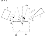
図7は、マーキング工程200で用いられるレーザーマーキング装置の構造を表す図である。レーザーマーキング装置1は、レーザ発振器3と、ガルバノミラー4,5と、ガルバノ6,7と、結像レンズ8と、テーブル9と、制御装置11と、ガルバノ制御部12と、ノズル13と、フード14とを備えている。
FIG. 7 is a diagram illustrating the structure of a laser marking device used in the
レーザ発振器3から出力されたレーザ光2は、ガルバノ6,7で駆動されるガルバノミラー4,5によりXY方向に走査され、結像レンズ8によってテーブル9に載置されたシリコンウエハ20のマーキング面22の上に結像される。これにより、チップ25の品種名やロット番号などの情報がマーキング面22にマーキングされる。
The
ガルバノミラー4,5によるレーザ光2のスキャンだけでは、シリコンウエハ20の限られた範囲にしか印字できないので、テーブル9によりシリコンウエハ20をXY方向に移動させて、マーキング面22の全体に順次印字する。
Since only the scanning of the
制御装置11は、レーザ発振器3の発振、停止、および発振出力を制御するとともに、テーブル9を駆動制御する。また、制御装置11は、ガルバノ制御部12に制御信号を送信する。ガルバノ制御部12は、制御装置11からの制御信号に基づいて、ガルバノ6,7を駆動制御する。
The
ノズル13は、不図示の不活性ガス供給装置に接続されており、マーキングの際、不活性ガス供給装置から供給される不活性ガス15をマーキング面22のレーザ照射範囲近傍に吹き込む。図7,8に示すように、ノズル13は、レーザ光2と干渉しないように、レーザ照射範囲から離れた位置に設けられ、レーザ光2の光軸2aがマーキング面22となす角度とは異なる角度で不活性ガス15をマーキング面22に対して吹きつける。不活性ガス15については後述する。本実施の形態では、ノズル13は、テーブル9の上面近傍に設けられているので、不活性ガス15をマーキング面22のレーザ照射範囲近傍でマーキング面22に対して略平行となるように、一定方向に吹き込むことができる。
The
フード14は、不図示の吸引装置に接続されており、ノズル13からマーキング面22に吹きつけられた不活性ガス15、および後述するシリコン粒子26を吸引する。フード14は、ノズル13と同様にレーザ光2と干渉しないように、レーザ照射範囲から離れた位置に設けられ、ノズル13からマーキング面22に吹きつけられた不活性ガス15の流れに対応する位置にノズル13と対向するように設けられている。本実施の形態では、フード14は、ノズル13と同様にテーブル9の上面近傍に設けられている。なお、図示はしないが、レーザーマーキング装置1は、ノズル13から吹き出された不活性ガス15が周囲に漏れないように、ノズル13やフード14を含めて、レーザ照射部分の全体が覆われている(不図示)。
The
マーキングの対象となるシリコンウエハ20のマーキング面22の状態は、シリコンウエハの製造工程の違いによって、機械的に研削された状態(バックグラインド仕上げ)であったり、酸化膜が形成された状態であったり、エッチングされた状態であったりする。本実施の形態では、バックグラインド仕上げが施されたシリコンウエハ20について説明する。図9(a)に示すように、シリコンウエハ20のマーキング面22、すなわち裏面には、バックグラインド仕上げによるバックグラインド痕22aが残っている。バックグラインド痕22aによる凹凸の深さは、約0.3μm程度である。
The marking
図9(b)に示すように、バックグラインド痕22aを溶融平坦化するようにレーザ光2を照射すると、照射された部分22bのバックグラインド痕22aが消失して平坦化するので、レーザ光2の照射部分22bは非照射部分と肉眼で識別可能となる。また、レーザ光2のエネルギー密度を上げることで、図9(c)に示すようにマーキング面22を彫り込むことによっても、レーザ光2の照射部分22bは非照射部分と肉眼で識別可能となる。
As shown in FIG. 9B, when the
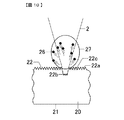
このように、レーザ光2によるマーキングでは、レーザ光2の照射によってマーキング面22のバックグラインド痕22aを平坦化、もしくは削り込むようにしてマーキングするので、照射部分22bからは、図10,11に示すようにシリコン粒子26が発生する。また、従来のレーザマーキング装置では、マーキング面22のレーザ照射範囲近傍の雰囲気は、周囲の大気と同じ雰囲気であるので、レーザ光2の照射によって照射部分22bの周囲にプラズマ27が発生する。そのため、マーキング面22にプラズマ27の熱が作用した部分(熱影響部)22cでは、ダイシングテープ30の粘着層31に対しての濡れ性が高くなってしまう。一般的に、粘着層31が貼り付けられる面の粘着層31に対する濡れ性が高いと、その面に対する粘着層31の粘着力は高くなる。
Thus, in marking with the
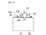
レーザ光2の照射を停止すると、プラズマ27が消滅するが、図11に示すように、プラズマ27の消滅に伴って、発生していたシリコン粒子26が高速でマーキング面22に打ち込まれてしまう。このように、従来のレーザマーキング装置では、照射部分22b(マーキング部)の周囲にプラズマ27による熱影響部22cと、マーキング面22に打ち込まれたシリコン粒子26とが生じる(図12)。
When the irradiation of the
図13(a)に示すように、従来のレーザマーキング装置でマーキングしたマーキング面22にダイシングテープ30を貼り付けてダイシングした後、紫外線を照射しても、熱影響部22cの粘着層31に対する濡れ性が高いため、粘着層31の粘着力は高い状態に保たれる。さらに、マーキング面22に打ち込まれたシリコン粒子26とが粘着層31に対してアンカーとしての効果を生じるため、図13(b),(c)に示すように、ダイシングテープ30をマーキング面22から剥がしても、粘着層31の一部は、マーキング面22に残ってしまう。また、チップ25がダイシングテープ30から剥がすことができず、ピックアップ自体ができないこともある。特に近年ではシリコンウエハ20が薄型化しているため、ピックアップの際にチップ25を破損する恐れもある。
As shown in FIG. 13A, even if the dicing
発明者らは、この問題を解決するために種々調査したところ、粘着層31がチップ25から剥離しにくくなる要因として上述した現象が関与していることを発見した。そこで、上述のように、本実施の形態のレーザマーキング装置1では、マーキングの際、ノズル13から不活性ガス15をマーキング面22のレーザ照射範囲近傍に吹き込むように構成した(図7,8)。不活性ガス15としては、窒素やアルゴン、ヘリウムなどのガスを用いることができる。なお、電離電位や熱伝導率が高く、プラズマ27の発生を抑制できる気体であれば、不活性ガス15の種類は、上述のものに限定されない。なお、不活性ガス15の代わりにエアを吹き込んでも、プラズマ27の発生の抑制効果が少ないため、粘着層31に対しての濡れ性が高くなることの防止効果を期待できない。
The inventors conducted various investigations to solve this problem, and found that the above-described phenomenon is involved as a factor that makes it difficult for the
本実施の形態のレーザマーキング装置1では、次の作用効果を奏する。
(1) マーキング面22のレーザ照射範囲近傍に不活性ガス15を吹きつけるよう構成した。これにより、マーキング面22のレーザ照射範囲近傍は不活性ガス雰囲気となり、プラズマ27の発生が抑制される。したがって、マーキング面22の粘着層31に対する濡れ性が高まることを防止でき、ダイシングテープ30からのチップ25の剥離性を向上できるので、粘着層31の残留やチップ25の破損といった不具合を防止して、チップ25の製造工程における歩留まりを向上でき、生産性を大きく向上できる。また、剥離性の向上によってピックアップ時にチップ25にかかる応力を低減できるので、チップ25の信頼性も向上できる。さらに、従来から行われているダイシングテープ30を利用したダイシング方法をそのまま適用できるので、製造装置のコスト増はわずかであり、経済的である。
The
(1) The
(2) マーキングの際に発生するシリコン粒子26を不活性ガス15の流れによって吹き飛ばすことができるので、シリコンウエハ20のマーキング面22にシリコン粒子26が付着せず、粘着層31に対するアンカー効果を防止でき、ピックアップの際のダイシングテープ30の剥離性向上に寄与できる。また、マーキング面22や結像レンズ8の表面の清浄性を保つことができる。
(2) Since the
(3) 不活性ガス15は、レーザ光2と干渉しないようにレーザ照射範囲から離れた位置に設けられたノズル13から、レーザ光2の光軸2aがマーキング面22となす角度とは異なる角度でマーキング面22に対して吹きつけられる。これにより、少ない不活性ガス15の噴射量でマーキング面22のレーザ照射範囲近傍を不活性ガス雰囲気とできるとともに、マーキングの際に発生するシリコン粒子26を効率よく吹き飛ばすことができるので、不活性ガス15の使用量を抑制でき、経済的である。
(3) The
(4) ノズル13からマーキング面22に吹きつけられた不活性ガス15の流れに対応する位置にノズル13と対向するようにフード14を設けて、ノズル13からマーキング面22に吹きつけられた不活性ガス15、およびシリコン粒子26を吸引するように構成した。これにより、吹きつけられた不活性ガス15と、不活性ガス15によって吹き飛ばされたシリコン粒子26を効率よく吸引できるので、吸引装置の能力を低く抑えることができ、装置コストを抑制できる。また、レーザ照射部分を囲うとともにフード14から効率よく不活性ガス15を吸引するので、不活性ガス15が外部へ漏れることを防止でき、安全性が高い。
(4) A
−−−変形例−−−
(1) 上述の説明では、ノズル13から不活性ガス15をマーキング面22のレーザ照射範囲近傍に吹き込むことでマーキング面22のレーザ照射範囲近傍を不活性ガス雰囲気としていたが、本発明はこれに限定されない。プラズマの発生を抑制するためにマーキング面22のレーザ照射範囲近傍が不活性ガス雰囲気であること、およびレーザ照射によって発生したシリコン粒子26をシリコンウエハ20の外に吹き飛ばす不活性ガス15の流れが生じていること、という条件を満たすものであればよい。例えば、気密の保たれたチャンバ内を不活性ガス15で満たすとともに、マーキング面22のレーザ照射範囲近傍においてシリコン粒子26を吹き飛ばすのに十分な流速で不活性ガス15の流れが発生するようチャンバ内の全体で不活性ガス15が流動するように構成してもよい。
---- Modified example ---
(1) In the above description, the
(2) 上述の説明では、シリコンウエハ20のマーキングについて説明したが、本発明はこれに限定されない。例えば、ダイヤモンドウエハや、シリコン・カーバイト系、ガリウム・ヒ素系、インジウム・リン系などの化合物半導体ウエハ、その他の材料からなる電子材料用途のウエハであっても良い。
(2) Although the marking of the
(3) 上述の説明では、半導体チップの製造工程におけるレーザマーキングについて説明したが、本発明はこれに限定されない。たとえば、MEMS(Micro Electro Mechanical System)技術を利用したマイクロマシンの製造工程に、レーザ光によってマーキングされたウエハのレーザマーキング面に粘着剤を貼り付けた後、チップ化して再び剥がすという操作が含まれていれば、そのマーキング工程に本発明を適用できる。すなわち、レーザ光によってマーキングされた対象物のレーザマーキング面に粘着剤を貼り付けた後、再び剥がすという操作を含む工程であれば、対象物は、半導体ウエハに限定されず、様々な対象物の製造工程に本発明を適用できる。さらに、上述したシリコン粒子26のようにレーザマーキングの際に発生する粒子がマーキング面に付着することによる弊害を防止するために本発明を適用してもよい。この場合、対象物は特に限定されず、レーザマーキング面に粘着剤の貼り付けや剥がしが行われないものであってもよい。
(4) 上述した各実施の形態および変形例は、それぞれ組み合わせてもよい。
(3) Although the laser marking in the semiconductor chip manufacturing process has been described in the above description, the present invention is not limited to this. For example, the manufacturing process of a micromachine using MEMS (Micro Electro Mechanical System) technology includes an operation in which an adhesive is applied to a laser marking surface of a wafer marked with laser light, and then is made into a chip and peeled off again. If so, the present invention can be applied to the marking process. In other words, the object is not limited to a semiconductor wafer as long as the process includes an operation of attaching an adhesive to the laser marking surface of an object marked with laser light and then removing it again. The present invention can be applied to a manufacturing process. Furthermore, the present invention may be applied to prevent adverse effects caused by particles generated during laser marking, such as the
(4) You may combine each embodiment and modification which were mentioned above, respectively.
以上の実施の形態およびその変形例において、たとえば、レーザ光源はレーザ発振器3に、吹き込み手段はノズル13に、吸引手段はフード14にそれぞれ対応する。さらに、本発明の特徴的な機能を損なわない限り、本発明は、上述した実施の形態における機器構成に何ら限定されない。
In the above embodiment and its modifications, for example, the laser light source corresponds to the
1 レーザーマーキング装置 2 レーザ光
3 レーザ発振器 13 ノズル
14 フード 20 シリコンウエハ
21 表面 22 裏面(マーキング面)
25 チップ 26 シリコン粒子
27 プラズマ 30 ダイシングテープ
31 粘着層 35 ダイサ
36 押上ピン 37 コレッット
DESCRIPTION OF
25
Claims (9)
前記マーキング面にダイシングテープを貼り付け、
前記ダイシングテープが貼り付けられたウエハを分割し、
前記分割されたウエハを前記ダイシングテープからチップとして取り出すことを特徴とするウエハの個片化方法。 Marking by irradiating a laser while blowing inert gas on the marking surface of the wafer before singulation into chips,
Affixing dicing tape on the marking surface,
Dividing the wafer to which the dicing tape is attached,
A method for separating wafers, wherein the divided wafers are taken out as chips from the dicing tape.
前記不活性ガスは、前記マーキング面におけるレーザ照射部分近傍に吹き込まれることを特徴とするウエハの個片化方法。 The wafer singulation method according to claim 1,
The wafer singulation method, wherein the inert gas is blown in the vicinity of a laser irradiation portion on the marking surface.
前記不活性ガスは、前記マーキング面に対して吹き込まれた後の前記不活性ガスの流れに対応する位置で吸引されることを特徴とするウエハの個片化方法。 The wafer singulation method according to claim 2,
The wafer singulation method, wherein the inert gas is sucked at a position corresponding to the flow of the inert gas after being blown into the marking surface.
前記チップは、電子材料デバイスであることを特徴とするウエハの個片化方法。 In the wafer singulation method according to any one of claims 1 to 3,
The method for separating wafers, wherein the chip is an electronic material device.
前記マーキング面におけるレーザ照射部分近傍の不活性ガスの流れが前記マーキング面と略平行となるように前記不活性ガスを吹き込む吹き込み手段とを備えることを特徴とするレーザマーキング装置。 A laser light source for irradiating a laser beam for marking the marking surface of the object;
A laser marking apparatus comprising: a blowing means for blowing the inert gas so that a flow of an inert gas in the vicinity of a laser irradiation portion on the marking surface is substantially parallel to the marking surface.
前記吹き込み手段は、前記マーキング面の近傍に設けられていることを特徴とするレーザマーキング装置。 In the laser marking device according to claim 7,
The laser marking apparatus, wherein the blowing means is provided in the vicinity of the marking surface.
前記マーキング面に対して吹きつけられた後の前記不活性ガスの流れに対応する位置で前記不活性ガスを吸引する吸引手段をさらに備えることを特徴とするレーザマーキング装置。 In the laser marking device according to claim 7 or 8,
The laser marking device further comprising suction means for sucking the inert gas at a position corresponding to the flow of the inert gas after being blown against the marking surface.
Priority Applications (1)
| Application Number | Priority Date | Filing Date | Title |
|---|---|---|---|
| JP2004109185A JP2005294636A (en) | 2004-04-01 | 2004-04-01 | Wafer singulation method, chip, laser marking method and laser marking apparatus |
Applications Claiming Priority (1)
| Application Number | Priority Date | Filing Date | Title |
|---|---|---|---|
| JP2004109185A JP2005294636A (en) | 2004-04-01 | 2004-04-01 | Wafer singulation method, chip, laser marking method and laser marking apparatus |
Publications (1)
| Publication Number | Publication Date |
|---|---|
| JP2005294636A true JP2005294636A (en) | 2005-10-20 |
Family
ID=35327210
Family Applications (1)
| Application Number | Title | Priority Date | Filing Date |
|---|---|---|---|
| JP2004109185A Pending JP2005294636A (en) | 2004-04-01 | 2004-04-01 | Wafer singulation method, chip, laser marking method and laser marking apparatus |
Country Status (1)
| Country | Link |
|---|---|
| JP (1) | JP2005294636A (en) |
Cited By (5)
| Publication number | Priority date | Publication date | Assignee | Title |
|---|---|---|---|---|
| JP2008084918A (en) * | 2006-09-26 | 2008-04-10 | Casio Comput Co Ltd | Mark forming method for semiconductor device |
| KR101528360B1 (en) * | 2014-01-07 | 2015-06-15 | 코리아테크노(주) | Marking unit and wafer sorter using the same |
| WO2016003005A1 (en) * | 2014-07-03 | 2016-01-07 | 주식회사 이오테크닉스 | Wafer marking method |
| JP2016533025A (en) * | 2013-09-19 | 2016-10-20 | アプライド マテリアルズ インコーポレイテッドApplied Materials,Incorporated | Wafer dicing from the back side and front side of the wafer |
| US10328529B2 (en) | 2015-08-26 | 2019-06-25 | Electro Scientific Industries, Inc | Laser scan sequencing and direction with respect to gas flow |
-
2004
- 2004-04-01 JP JP2004109185A patent/JP2005294636A/en active Pending
Cited By (8)
| Publication number | Priority date | Publication date | Assignee | Title |
|---|---|---|---|---|
| JP2008084918A (en) * | 2006-09-26 | 2008-04-10 | Casio Comput Co Ltd | Mark forming method for semiconductor device |
| JP2016533025A (en) * | 2013-09-19 | 2016-10-20 | アプライド マテリアルズ インコーポレイテッドApplied Materials,Incorporated | Wafer dicing from the back side and front side of the wafer |
| KR101528360B1 (en) * | 2014-01-07 | 2015-06-15 | 코리아테크노(주) | Marking unit and wafer sorter using the same |
| WO2016003005A1 (en) * | 2014-07-03 | 2016-01-07 | 주식회사 이오테크닉스 | Wafer marking method |
| CN106463497A (en) * | 2014-07-03 | 2017-02-22 | Eo科技股份有限公司 | Wafer marking method |
| US10304778B2 (en) | 2014-07-03 | 2019-05-28 | Eo Technics Co., Ltd | Wafer marking method |
| CN106463497B (en) * | 2014-07-03 | 2019-10-22 | Eo科技股份有限公司 | Wafer marking method |
| US10328529B2 (en) | 2015-08-26 | 2019-06-25 | Electro Scientific Industries, Inc | Laser scan sequencing and direction with respect to gas flow |
Similar Documents
| Publication | Publication Date | Title |
|---|---|---|
| JP4544231B2 (en) | Manufacturing method of semiconductor chip | |
| JP5307384B2 (en) | Wafer division method | |
| US7446022B2 (en) | Wafer laser processing method | |
| CN100466184C (en) | wafer processing method | |
| CN111512423B (en) | Mounting method and mounting device | |
| JP5710133B2 (en) | How to divide work | |
| US7605058B2 (en) | Wafer dividing method | |
| US7888239B2 (en) | Semiconductor device manufacturing method | |
| US7544588B2 (en) | Laser processing method for wafer | |
| CN104078425B (en) | The processing method of chip | |
| JP2009200140A (en) | Method of manufacturing semiconductor chip | |
| CN104517898A (en) | Wafer processing method | |
| CN107039341A (en) | The processing method of chip | |
| JP2006229021A (en) | Wafer division method | |
| JP2007157887A (en) | Wafer division method | |
| KR20140136875A (en) | Laser machining apparatus | |
| JP2005332931A (en) | Wafer mounter | |
| JP2005228794A (en) | Method of manufacturing chip | |
| JP2005294636A (en) | Wafer singulation method, chip, laser marking method and laser marking apparatus | |
| JP2014013807A (en) | Wafer processing method | |
| JP2006245209A (en) | Manufacturing method of semiconductor chip | |
| JP2014011381A (en) | Wafer processing method | |
| JP7358193B2 (en) | Wafer processing method | |
| JP2005276987A (en) | Ultra-thin chip manufacturing process and manufacturing equipment | |
| JP4114196B2 (en) | Method of peeling electronic component and mounting method thereof |