JP2005294629A - Manufacturing method of display device - Google Patents
Manufacturing method of display device Download PDFInfo
- Publication number
- JP2005294629A JP2005294629A JP2004109095A JP2004109095A JP2005294629A JP 2005294629 A JP2005294629 A JP 2005294629A JP 2004109095 A JP2004109095 A JP 2004109095A JP 2004109095 A JP2004109095 A JP 2004109095A JP 2005294629 A JP2005294629 A JP 2005294629A
- Authority
- JP
- Japan
- Prior art keywords
- wiring
- layer
- display device
- substrate
- conductive
- Prior art date
- Legal status (The legal status is an assumption and is not a legal conclusion. Google has not performed a legal analysis and makes no representation as to the accuracy of the status listed.)
- Pending
Links
Images
Landscapes
- Liquid Crystal (AREA)
- Thin Film Transistor (AREA)
- Electrochromic Elements, Electrophoresis, Or Variable Reflection Or Absorption Elements (AREA)
- Devices For Indicating Variable Information By Combining Individual Elements (AREA)
Abstract
【課題】 表示装置の製造工程、特に表示装置用マトリクスアレイ基板の製造工程における静電破壊に対する耐性をより向上させることができる表示装置の製造方法を提供する。
【解決手段】 表示装置は、少なくとも一表面上に絶縁層101が形成された導電性の金属基板100と、金属基板100の絶縁層101が形成されている面側にマトリクス状に形成されたゲート配線106およびソース配線111と、金属基板100の上記面側にさらに形成された、ゲート配線106に接続されたゲートショート配線105およびソース配線111に接続されたソースショート配線104とを備えたマトリクスアレイ基板を有している。この表示装置の製造方法は、少なくともマトリクスアレイ基板の製造工程において、金属基板100とゲートショート配線105およびソースショート配線104とをコンタクトホール102,103を介して電気的に接続する工程を有している。
【選択図】 図1PROBLEM TO BE SOLVED: To provide a display device manufacturing method capable of further improving resistance to electrostatic breakdown in a manufacturing process of a display device, particularly a manufacturing process of a matrix array substrate for a display device.
A display device includes a conductive metal substrate 100 in which an insulating layer 101 is formed on at least one surface, and gates formed in a matrix on the surface side of the metal substrate 100 where the insulating layer 101 is formed. A matrix array including a wiring 106 and a source wiring 111, and a gate short wiring 105 connected to the gate wiring 106 and a source short wiring 104 connected to the source wiring 111, which are further formed on the surface side of the metal substrate 100. It has a substrate. This display device manufacturing method includes a step of electrically connecting the metal substrate 100 to the gate short wiring 105 and the source short wiring 104 via the contact holes 102 and 103 at least in the manufacturing process of the matrix array substrate. Yes.
[Selection] Figure 1
Description
本発明は、表示装置の製造方法等に関し、さらに詳しくは、絶縁層又は絶縁体により絶縁された導電性基板上にマトリクス配線を有する表示装置の製造方法等に関する。 The present invention relates to a method for manufacturing a display device, and more particularly to a method for manufacturing a display device having a matrix wiring on a conductive substrate insulated by an insulating layer or an insulator.
薄膜トランジスタ(以下、TFT(Thin Film Transistor)と記す。)は、液晶表示素子やエレクトロルミネッセント(EL)表示素子、または電気泳動表示装置用のアクティブマトリクス基板として用いられ、例えば電気泳動表示装置においては、各画素において泳動液内に封入されたトナーに電界をかけるために制御電極電位を制御するための素子として用いられる。 A thin film transistor (hereinafter referred to as TFT (Thin Film Transistor)) is used as an active matrix substrate for a liquid crystal display element, an electroluminescent (EL) display element, or an electrophoretic display device, for example, in an electrophoretic display device Is used as an element for controlling the control electrode potential in order to apply an electric field to the toner sealed in the electrophoresis solution in each pixel.
各画素に設けたTFTに用いられる半導体膜には非晶質のシリコン薄膜(a−Si薄膜)や多結晶のシリコン薄膜(poly−Si薄膜)がある。 A semiconductor film used for a TFT provided in each pixel includes an amorphous silicon thin film (a-Si thin film) and a polycrystalline silicon thin film (poly-Si thin film).
従来、これらの技術では、例えば表示装置である液晶ディスプレイ用途ではガラスを基板として用いることが多く、それゆえ、使用用途にもよるが、表示装置は耐衝撃性や柔軟性が十分ではない。 Conventionally, in these technologies, for example, glass is often used as a substrate in a liquid crystal display application that is a display device, and therefore the display device has insufficient impact resistance and flexibility, depending on the application.
また、昨今では、上述したような電気泳動表示装置を用いた、従来では実現し得なかった、薄く、丈夫で、かつ紙のようなしなやかさを備えたディスプレイの開発も盛んに行われている。それに伴い、表示素子を駆動するためのTFTバックプレーンを、従来のガラス基板ではなく、割れにくく丈夫な、可撓性のある薄い金属板やプラスチック板の上に形成することが考えられている。 In addition, in recent years, the development of a thin, durable, and supple paper-like display that could not be realized by using an electrophoretic display device as described above has been actively conducted. . Accordingly, it is considered to form a TFT backplane for driving the display element on a flexible thin metal plate or plastic plate that is hard to break and is not a conventional glass substrate.
ところで、導電性材料の一つであるステンレス鋼(以下、SUS(Steel Use Stainless)と記す。)からなる導電性基板を用いた場合は、現在多く用いられているガラス基板や、現在検討が進められているプラスチック板やプラスチックフィルムを基板とした場合と大きく異なる点がある。すなわち、導電性基板を前述したような表示装置用の基板として用いる場合には、少なくとも導電性基板の機能面を絶縁加工する必要がある。導電性基板の機能面を絶縁加工する技術は、例えば特許文献1に開示されている。 By the way, in the case of using a conductive substrate made of stainless steel (hereinafter referred to as SUS (Steel Use Stainless)), which is one of the conductive materials, a glass substrate that is widely used at present, and studies are now underway. There is a significant difference from the case of using a plastic plate or plastic film as a substrate. That is, when the conductive substrate is used as a substrate for a display device as described above, it is necessary to insulate at least the functional surface of the conductive substrate. A technique for insulating the functional surface of a conductive substrate is disclosed in Patent Document 1, for example.
導電性基板を絶縁加工する方法としては、酸化膜を成膜するなどの幾つかの方法が考えられる。その他にも、例えば、窒化シリコン層を導電性基板上に成膜し、その上に走査電極または情報電極を形成する方法が考えられる。 As a method for insulating the conductive substrate, several methods such as forming an oxide film are conceivable. In addition, for example, a method of forming a silicon nitride layer on a conductive substrate and forming a scan electrode or an information electrode thereon can be considered.
このような、アクティブマトリクス基板の製造工程において、例えば液晶ディスプレイ(LCD)用途であればラビング工程、その他のデバイスにおいても製造工程中に静電気が生じ、マトリクス配線間の絶縁破壊や、アクティブ素子を有する場合は電気的特性の変化が生じることがある。そのため、従来では、各配線、各素子、または各配線と各素子とを同電位にするために、それらをいわゆるショートリングに電気的に接続した状態で製造が行われている。
しかしながら、導電性基板を用いた場合に、従来のように、各配線や各素子電極の電位を同電位とするためにそれらをショートリングに電気的に接続した状態で製造を行ったとしても、基板絶縁層をはさむ導電性基板と各電極または各素子電極等との間に依然として電位差が生じ、基板絶縁層が部分的に破壊されてしまう場合がある。その結果、基板配線間にショートが生じたり、アクティブ素子を有する場合においてはそのアクティブ素子の電気的特性が変化したりするなどの問題が依然として生じてしまうこととなる。 However, when a conductive substrate is used, even if manufacturing is performed in a state where they are electrically connected to a short ring in order to make the potential of each wiring or each element electrode the same potential as in the past, There may still be a potential difference between the conductive substrate sandwiching the substrate insulating layer and each electrode or each element electrode, and the substrate insulating layer may be partially destroyed. As a result, problems such as a short circuit between the substrate wirings and a change in the electrical characteristics of the active element still occur when the active element is provided.
そこで本発明は、表示装置の製造工程、特に表示装置用マトリクスアレイ基板の製造工程における静電破壊に対する耐性をより向上させることができる表示装置の製造方法等を提供することを目的とする。 Accordingly, an object of the present invention is to provide a display device manufacturing method and the like that can further improve resistance to electrostatic breakdown in a display device manufacturing process, in particular, a display device matrix array substrate manufacturing process.
上記目的を達成するため、本発明の表示装置用マトリクスアレイ基板の製造方法は、少なくとも一表面上に絶縁層が形成された導電性基板と、該導電性基板の前記絶縁層が形成されている面側にマトリクス状に形成された走査電極および情報電極と、前記導電性基板の前記面側にさらに形成された、前記走査電極に接続された第1の配線および前記情報電極に接続された第2の配線と、を備えた表示装置用マトリクスアレイ基板の製造方法において、少なくとも前記マトリクスアレイ基板の製造工程において、前記導電性基板と少なくとも前記第1または第2の配線のいずれかとを電気的に接続する工程を有していることを特徴とする。 In order to achieve the above object, a method of manufacturing a matrix array substrate for a display device according to the present invention includes a conductive substrate having an insulating layer formed on at least one surface and the insulating layer of the conductive substrate. Scan electrodes and information electrodes formed in a matrix on the surface side, and first wiring connected to the scan electrodes and further connected to the information electrodes, further formed on the surface side of the conductive substrate In the method of manufacturing a matrix array substrate for a display device comprising two wirings, at least in the manufacturing process of the matrix array substrate, the conductive substrate and at least one of the first and second wirings are electrically connected It has the process of connecting, It is characterized by the above-mentioned.
また、本発明に係る表示装置の製造方法は、導電性基板上に複数のアクティブ素子が構成されてなるマトリクスアレイ基板を有する表示装置の製造方法であって、前記導電性基板の一表面上に第1の絶縁層を形成する工程と、該第1の絶縁層に第1のコンタクトホールを形成する工程と、前記第1の絶縁層上および前記第1のコンタクトホール内に第1の導電層を形成し、該第1の導電層をパターニングすることによって、第1の配線を形成する工程と、該第1の配線の上に第2の絶縁層および半導体層を形成する工程と、前記第2の絶縁層および前記半導体層に第2のコンタクトホールを形成する工程と、少なくとも該第2のコンタクトホールを含む領域に第2の導電層を形成し、該第2の導電層をパターンニングすることによって第2の配線を形成し、前記導電性基板と前記第1の配線と前記第2の配線とを前記第1および第2のコンタクトホールを介して電気的に接続する工程と、を含むことを特徴とする。 The display device manufacturing method according to the present invention is a method for manufacturing a display device having a matrix array substrate in which a plurality of active elements are formed on a conductive substrate, on a surface of the conductive substrate. Forming a first insulating layer; forming a first contact hole in the first insulating layer; and a first conductive layer on the first insulating layer and in the first contact hole. Forming a first wiring by patterning the first conductive layer, forming a second insulating layer and a semiconductor layer on the first wiring, and Forming a second contact hole in the two insulating layers and the semiconductor layer, forming a second conductive layer in a region including at least the second contact hole, and patterning the second conductive layer Second by Forming a line, and electrically connecting the conductive substrate, the first wiring, and the second wiring through the first and second contact holes. .
上記のような本発明の製造方法によれば、マトリクスアレイ基板の製造工程中、導電性基板と第1の配線と第2の配線とが第1および第2のコンタクトホールを介して電気的に接続されるので、それらが略同電位に保たれる。そのため、例えば、製造工程中に生じる静電気によって静電破壊が生じて、導電性基板と第1または第2の配線との間でショートが生じるようなことがないので、製造工程における静電破壊に対する耐性をより向上させることが可能になる。 According to the manufacturing method of the present invention as described above, during the manufacturing process of the matrix array substrate, the conductive substrate, the first wiring, and the second wiring are electrically connected via the first and second contact holes. Since they are connected, they are kept at substantially the same potential. Therefore, for example, there is no case where electrostatic breakdown occurs due to static electricity generated during the manufacturing process, and a short circuit does not occur between the conductive substrate and the first or second wiring. Resistance can be further improved.
また、本発明の情報機器は、上記本発明の表示装置の製造方法を用いて製造された表示装置を有する。 Moreover, the information apparatus of this invention has the display apparatus manufactured using the manufacturing method of the display apparatus of the said invention.
以上説明したように、本発明の製造方法によれば、表示装置の製造工程、特に表示装置用マトリクスアレイ基板の製造工程における静電破壊に対する耐性をより向上させることができる。 As described above, according to the manufacturing method of the present invention, it is possible to further improve the resistance to electrostatic breakdown in the manufacturing process of the display device, particularly in the manufacturing process of the matrix array substrate for display device.
次に、本発明の実施形態について図面を参照して説明する。 Next, embodiments of the present invention will be described with reference to the drawings.
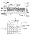
図1(a)は本発明の一実施形態に係る表示装置におけるマトリクスアレイ基板の一部の断面を模式的に示す図であり、図1(b)は本実施形態の表示装置における300行×250列のTFTアクティブマトリクスアレイ基板の一部分を示す模式図である。なお、図1(a)のA部分は図1(b)におけるA領域の断面を示し、図1(a)のB部分は図1(b)におけるB領域の断面を示している。 FIG. 1A is a diagram schematically showing a cross section of a part of a matrix array substrate in a display device according to an embodiment of the present invention, and FIG. It is a schematic diagram which shows a part of 250 rows TFT active matrix array substrate. 1A shows a cross section of the A region in FIG. 1B, and B portion of FIG. 1A shows a cross section of the B region in FIG. 1B.
図1(a)に示すように、本実施形態に係る表示装置は、導電性基板としての薄型の金属基板100上に、例えばプラズマCVD(Chemical Vapor Deposition)法により形成されたSiN等からなる第1の絶縁層101が設けられている。金属基板100のうち、いわゆるショートリングが形成され製造工程後に切り離される領域(図1(b)のカットライン123の外側の領域)に設けられている第1の絶縁層101には、第1のコンタクトホールである基板絶縁層コンタクトホール102が形成されている。この基板絶縁層コンタクトホール102は、例えばエッチングプロセスによって形成される。
As shown in FIG. 1A, the display device according to the present embodiment includes, for example, SiN formed by, for example, plasma CVD (Chemical Vapor Deposition) on a
第1の絶縁層101の上には、表示装置が例えばボトムゲート構成のTFTを備えた構成の場合には、走査電極としてのゲート配線106、ゲート配線106が接続された第1のショート配線としてのゲートショート配線105、およびCs(補助容量)配線107が形成されている。
On the first
ここで、これらの配線105,106,107の形成方法について簡単に説明すると、これらの配線の材料として例えば抵抗率が比較的低いAlを用いて配線層を形成し、その後のプロセスにAlの融点を超えるようなプロセスがある場合は、その配線層の上にCr、Ta、あるいはAl−Ndをスパッタリングによって蒸着させて導電膜を形成する。続いて、その導電膜の上にレジストを塗布してこれを選択的に露光および現像し、導電膜をエッチングによって所定の形状にパターニングする。以上により、配線105,106,107が形成される。
Here, a method for forming these
それらの配線105,106,107の上には第2の絶縁層108が形成され、さらにその上にはアモルファス半導体層109が形成されている。金属基板100のうち、いわゆるショートリングが形成され製造工程後に切り離される領域における第2の絶縁層108およびアモルファス半導体層109には、第2のコンタクトホールであるゲート絶縁層コンタクトホール103が形成されている。このゲート絶縁層コンタクトホール103は、例えばエッチングプロセスによって形成される。
A second
第2の絶縁層108上には、例えばイオン注入法によって形成された後に選択除去されたオーミック接触層110が形成されている。さらに、それらの層の上には、情報電極としてのソース配線111(図1(b)参照)、ソース配線111が接続された第2のショート配線としてのソースショート配線104、およびドレイン電極112が形成されている。
On the second
第1のショート配線であるゲートショート配線105と、前記第2のショート配線ソースショート配線104とは、互いに交差するクロス部を形成するように、互いに異なる導電層に形成されている。ゲート絶縁層コンタクトホール103はそのクロス部に形成されており、これらのショート配線104,105はそのクロス部においてゲート絶縁層コンタクトホール103を介して互いに電気的に接続されている。
The gate
なお、ゲートショート配線105とソースショート配線104はカットライン123の外側に設けられており、これらのショート配線104,105とコンタクトホール102,103は製造工程終了後に金属基板100から切り離される。これらショート配線104,105および導電性基板100は、例えば、実装端子の先で電気的に接続されている。
The gate
このように、本実施形態の表示装置は、導電性の薄型の金属基板100上に基板絶縁層101を形成し、続いてその上にTFTマトリクスアレイを形成したマトリクスアレイ基板を備えており、少なくともそのマトリクスアレイ基板の製造工程中は、金属基板100と各ゲート配線106と各ソース配線111とが、ショート配線104,105およびコンタクトホール102,103を介して互いに電気的に接続されている。なお、TFTマトリクスアレイ基板の形態で出荷する場合などは、上記の電気的な接続を保った状態で出荷すれば、製品の輸送中に生じる静電気等に対しても耐性を有することになるので好ましい。また、上述の方法でショート配線、導電性基板を接続するのが好ましいが、導電性基板とゲートショート配線、ソースショート配線の少なくとも一方とがショート配線のクロス部以外でコンタクトホールを形成して接続されていてもよい。
As described above, the display device of this embodiment includes a matrix array substrate in which the
図1(b)に示すように、本実施形態の表示装置におけるTFTマトリクスアレイ基板には、複数のゲート配線106と複数のソース配線111とがマトリクス状に配置されている。ゲート配線106とソース配線111とに囲まれた各領域には、アクティブ素子であるTFT130が設けられている。各TFT130のドレイン電極側には画素電極114が接続されている。
As shown in FIG. 1B, a plurality of gate lines 106 and a plurality of
本実施形態の表示装置についてさらに詳細に説明する。 The display device of this embodiment will be described in more detail.
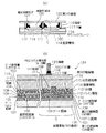
図2(a)は本発明の一実施形態に係る表示装置の一部の表示画素の断面を模式的に示す図であり、図2(b)は主に図2(a)におけるC部を拡大して示す断面図である。 FIG. 2A is a diagram schematically showing a cross section of a part of the display pixels of the display device according to the embodiment of the present invention, and FIG. It is sectional drawing expanded and shown.
図2(a)に示すように、本実施形態の表示装置は、金属基板100上に構成されたTFTバックプレーン124上の隔壁119に、第2の基板122が接合されている。隔壁119によって仕切られた各画素空間には、メモリー性を有する表示素子として、絶縁性液体120中に電気泳動粒子121を分散させてなる分散液(電気泳動表示素子)が設けられている。各画素の電気泳動表示素子は、TFTバックプレーン124上に画素ごとに設けられた画素電極114とTi層117とからなる一対の電極によって駆動される。より具体的に説明すると、本実施形態の表示装置は、画素電極114とTi層117とに正負の電圧を印加して、電気泳動粒子121を画素電極114の形成面と隔壁119の近傍との間を移動させることによって電気泳動表示素子を駆動し、表示を行う。なお、図2(a)は、電気泳動粒子121がTi層117に引き寄せられて隔壁119の近傍に移動した状態を示している。
As shown in FIG. 2A, in the display device of this embodiment, the second substrate 122 is bonded to the partition wall 119 on the TFT back
以下に、図2を参照しながら、本実施形態の表示装置の製造工程について説明する。
(1)まず、厚さ0.2mmのSUSからなる導電性基板としての金属基板100上に、CVD法によって、第1の絶縁層としてのSiN膜101を500nmの厚さに成膜する。
(2)金属基板100のうち、いわゆるショートリングが形成され製造工程後に切り離される領域(図1(b)のカットライン123の外側の領域)に設けられているSiN膜101に、ドライエッチングによって基板絶縁層コンタクトホール102を形成し、金属基板100の一部を露出させる。
(3)SiN膜101上に、Al−Ndをスパッタリングによって200nmの厚さに成膜して第1の導電層を形成し、フォトマスク(不図示)を用いてこの第1の導電層をウェットエッチングすることにより、ゲート配線106、各ゲート配線106を電気的に同電位とするためのゲートショート配線105、およびCs配線107を形成する。これと同時に、基板絶縁層コンタクトホール102を介して、ゲートショート配線105と金属基板100とを電気的に接続する。
Hereinafter, the manufacturing process of the display device of this embodiment will be described with reference to FIG.
(1) First, a
(2) Of the
(3) On the
なお、本実施形態のような電気泳動表示装置はTFT130の保持駆動を行う際の補助容量を必要とするため、ゲート配線106と同じ導電層にCs(補助容量)配線107を形成している。
(4)それらの配線105,106,107の上に、層間絶縁膜としてSiN膜108を250nmの厚さにCVDによって成膜し、さらにその上に、アモルファス半導体層としてa−Si膜109を200nmの厚さにCVDによって成膜する。
(5)金属基板100のうち、いわゆるショートリングが形成され、製造工程後に切り離される領域における絶縁層108およびアモルファス半導体層109に、ドライエッチングによってゲート絶縁層コンタクトホール103を形成する。
(6)絶縁層108およびアモルファス半導体層109上の所定の領域に、オーミック接触層として、a−Si(n+)膜110を20nmの厚さにCVDによって成膜する。
(7)オーミック接触層110の上にAl−Ndを200nmの厚さにスパッタリングによって成膜して、第2の導電層を形成する。
(8)この第2の導電層をフォトマスク(不図示)を用いてウェットエッチングすることによって、TFT部分を含むソース配線111、ドレイン電極112、および各ソース配線111群を電気的に同電位とするために互いに電気的に接続するソースショート配線104を形成する。この段階で、ソースショート配線104とゲートショート配線105とがゲート絶縁層コンタクトホール103を介して接続され、これにより、ソースショート配線104とゲートショート配線105と金属基板100とがコンタクトホール102,103を介して電気的に接続される。
Note that since the electrophoretic display device as in the present embodiment requires an auxiliary capacitor for holding and driving the TFT 130, the Cs (auxiliary capacitor)
(4) On these
(5) A gate insulating layer contact hole 103 is formed by dry etching in the insulating
(6) In a predetermined region on the insulating
(7) On the
(8) The second conductive layer is wet-etched using a photomask (not shown), so that the
引き続いて、所定のレジストパターンを用いたドライエッチングによってTFTチャネル部のa−Si(n+)層110を除去して半導体層109の一部を露出させ、上記配線104,111,112および一部が露出した半導体層109の上にパッシベーション層としてのSiN膜113を300nmの厚さに成膜する。
(9)SiN膜113に、ドライエッチングによって図2(b)のX部に示すように第3のコンタクトホールを形成し、ドレイン電極112の一部を露出させる。
(10)一部が露出したドレイン電極112およびSiN膜113の上にAl−Ndを200nmの厚さにスパッタリングによって成膜し、第3の導電層を形成する。
(11)フォトマスク(不図示)を用い、この第3の導電層をウェットエッチングによってパターニングして画素電極114を形成する。
(12)金属基板100上の上記構成の最上面上に、TiO2を含有したアクリル樹脂を4μmの厚さに塗布し、白色散乱層115を形成する。
(13)白色散乱層115の上にアクリル系の樹脂を1μmの厚さに成膜して、第3の絶縁層116を形成する。
(14)第3の絶縁層116の上に、Tiを300nmの厚さに成膜して金属層としてのTi層117を形成し、さらにその上に、第1のフォトレジスト層としてカーボンを含有したフォトレジスト層118を300nmの厚さに成膜する。
(15)次に、フォトレジスト層118の上に第2のフォトレジスト層として厚膜フォトレジスト層を15μmの厚さに形成し、厚膜フォトレジスト層が画素間の隔壁119を構成するように、この厚膜フォトレジスト層を画素間の部分を残して現像除去する。
(16)厚膜フォトレジスト層で形成された隔壁119を用いて、Ti層117とフォトレジスト層118とをエッチングし、TFTバックプレーン124を形成する。
(17)次に、パラフィン系炭化水素溶媒を主成分とする絶縁性液体120中に、カーボンブラックを含有したポリスチレン樹脂から成る黒色の電気泳動粒子120を分散させた分散液を、隔壁119で区画された空間内に充填し、透明な第2の基板122を隔壁119上に接着剤(不図示)によって固定する。
(18)最後に、金属基板100をカットライン123(図1(b))で切断し、各ゲート配線106および各ソース配線111と金属基板100とを電気的に接続しているショートリング部を金属基板100から切り離す。
Subsequently, the a-Si (n + )
(9) A third contact hole is formed in the
(10) A third conductive layer is formed by sputtering Al—Nd to a thickness of 200 nm on the
(11) A
(12) On the uppermost surface of the above configuration on the
(13) An acrylic resin film is formed to a thickness of 1 μm on the white scattering layer 115 to form the third insulating
(14) On the third insulating
(15) Next, a thick photoresist layer is formed as a second photoresist layer to a thickness of 15 μm on the
(16) Using the partition wall 119 formed of a thick photoresist layer, the
(17) Next, a dispersion liquid in which black electrophoretic particles 120 made of polystyrene resin containing carbon black are dispersed in an insulating liquid 120 containing a paraffinic hydrocarbon solvent as a main component is partitioned by partition walls 119. The transparent second substrate 122 is fixed on the partition wall 119 with an adhesive (not shown).
(18) Finally, the
以上により、本実施形態の表示装置の製造工程が完了する。 Thus, the manufacturing process of the display device of this embodiment is completed.
上述したように、本実施形態によれば、少なくともマトリクスアレイ基板の製造工程において、ソースショート配線104とゲートショート配線105と金属基板100とがコンタクトホール102,103を介して電気的に連通し、それらが略同電位に保たれている。そのため、製造工程中に生じる静電気によって基板絶縁層の静電破壊が生じて、例えば、金属基板100とゲート配線106との間でのショートや、金属基板100とソース配線111との間のショートが生じるようなことがないので、表示装置の製造工程における静電破壊に対する耐性をより向上させることが可能になり、TFTバックプレーンを導電性基板上に構成した場合においても良好な画質の表示装置を製造することができる。
As described above, according to the present embodiment, at least in the manufacturing process of the matrix array substrate, the source
なお、本実施形態では電気泳動表示装置のTFTバックプレーンの場合について説明したが、本発明を適用できるのはこれに留まらず、例えば反射型の液晶表示装置に応用することも可能である。この場合、例えば第2の基板122にITO(Indium Tin Oxide)膜のような透明な導電膜を形成してコモン電極を構成し、ドレイン電極との間に液晶を挟持し、ドレイン電極−コモン電極間に所望の電界をかけることで表示を行うことが可能である。 In this embodiment, the case of the TFT backplane of the electrophoretic display device has been described. However, the present invention can be applied to, for example, a reflective liquid crystal display device. In this case, for example, a transparent conductive film such as an ITO (Indium Tin Oxide) film is formed on the second substrate 122 to form a common electrode, and a liquid crystal is sandwiched between the drain electrode and the drain electrode-common electrode. It is possible to perform display by applying a desired electric field therebetween.
また、本実施形態ではアモルファスシリコンを用いた逆スタガー型のいわゆるボトムゲート型の構成を採用しているが、これに代えて、例えばトップゲート型の構成等を採用しても何ら問題はない。加えて、アモルファスシリコンを用いたTFTに限らず、例えば、レーザーアニールを用いたポリシリコンTFTや、単結晶TFTの転写技術を用いても良い。 In this embodiment, a reverse stagger type so-called bottom gate type configuration using amorphous silicon is employed, but there is no problem even if a top gate type configuration or the like is employed instead. In addition to the TFT using amorphous silicon, for example, a polysilicon TFT using laser annealing or a transfer technique of a single crystal TFT may be used.
また、上記の製造方法によって製造した本実施形態の電気泳動表示装置は、薄く形成することができ、また、ある程度の折り曲げに対応できるようなフレキシブルな構成になっているため、各種の情報機器用の表示装置として好適に用いられる。例えば、紙媒体に置き換えられるような用途や、情報携帯端末(PDA)のような情報端末の表示用ディスプレイとしても用いることができる。 In addition, the electrophoretic display device of the present embodiment manufactured by the above manufacturing method can be formed thin and has a flexible configuration that can cope with a certain degree of bending. It is suitably used as a display device. For example, it can be used as a display for an application such as a paper medium or an information terminal such as a personal digital assistant (PDA).
本発明は、薄型でフレキシブルな表示装置の製造方法、およびそのような製造方法を用いて製造された表示装置を有する情報機器に適用可能である。 The present invention can be applied to a method for manufacturing a thin and flexible display device, and information equipment having a display device manufactured using such a manufacturing method.
100 金属基板(SUS基板)
101 第1の絶縁層(SiN膜)
102 基板絶縁層コンタクトホール
103 ゲート絶縁層コンタクトホール
104 ソースショート配線
105 ゲートショート配線
106 ゲート配線
107 Cs配線
108 第2の絶縁層(SiN膜)
109 アモルファス半導体層(a−Si膜)
110 オーミック接触層(a−Si(n+)膜)
119 隔壁
120 絶縁性液体
121 電気泳動粒子
122 第2の基板
123 カットライン
124 TFTバックプレーン
130 TFT
100 Metal substrate (SUS substrate)
101 First insulating layer (SiN film)
102 Substrate insulating layer contact hole 103 Gate insulating
109 Amorphous semiconductor layer (a-Si film)
110 Ohmic contact layer (a-Si (n + ) film)
119 Partition 120 Insulating liquid 121 Electrophoretic particle 122 Second substrate 123
Claims (8)
少なくとも前記マトリクスアレイ基板の製造工程において、前記導電性基板と少なくとも前記第1または第2の配線のいずれかとを電気的に接続する工程を有していることを特徴とする表示装置用マトリクスアレイ基板の製造方法。 A conductive substrate having an insulating layer formed on at least one surface; a scanning electrode and an information electrode formed in a matrix on the surface of the conductive substrate on which the insulating layer is formed; and In a method of manufacturing a matrix array substrate for a display device, further comprising a first wiring connected to the scan electrode and a second wiring connected to the information electrode, further formed on the surface side,
A matrix array substrate for a display device, comprising at least a step of electrically connecting the conductive substrate and at least one of the first and second wirings in a manufacturing process of the matrix array substrate Manufacturing method.
前記導電性基板の一表面上に第1の絶縁層を形成する工程と、
該第1の絶縁層に第1のコンタクトホールを形成する工程と、
前記第1の絶縁層上および前記第1のコンタクトホール内に第1の導電層を形成し、該第1の導電層をパターニングすることによって、第1の配線を形成する工程と、
該第1の配線の上に第2の絶縁層および半導体層を形成する工程と、
前記第2の絶縁層および前記半導体層に第2のコンタクトホールを形成する工程と、
少なくとも該第2のコンタクトホールを含む領域に第2の導電層を形成し、該第2の導電層をパターンニングすることによって第2の配線を形成し、前記導電性基板と前記第1の配線と前記第2の配線とを前記第1および第2のコンタクトホールを介して電気的に接続する工程と、
を含むことを特徴とする表示装置の製造方法。 A method of manufacturing a display device having a matrix array substrate in which a plurality of active elements are formed on a conductive substrate,
Forming a first insulating layer on one surface of the conductive substrate;
Forming a first contact hole in the first insulating layer;
Forming a first conductive layer on the first insulating layer and in the first contact hole, and patterning the first conductive layer to form a first wiring;
Forming a second insulating layer and a semiconductor layer on the first wiring;
Forming a second contact hole in the second insulating layer and the semiconductor layer;
A second conductive layer is formed at least in a region including the second contact hole, and a second wiring is formed by patterning the second conductive layer, and the conductive substrate and the first wiring are formed. Electrically connecting the second wiring and the second wiring through the first and second contact holes;
A method for manufacturing a display device, comprising:
該パッシベーション層に第3のコンタクトホールを形成し、少なくとも該第3のコンタクトホールを含む領域に第3の導電層を形成し、該第3の導電層をパターンニングして画素電極を形成する工程と、
前記導電性基板上の構成の最上面上に白色散乱層を形成する工程と、
該白色散乱層上に第3の絶縁層を形成する工程と、
該第3の絶縁層上に金属層、第1のフォトレジスト層、および第2のフォトレジスト層を順に形成した後に、該金属層、該第1のフォトレジスト層、および該第2のフォトレジスト層をパターニングして隔壁を形成する工程と、
前記隔壁で仕切られた空間内に、絶縁性液体中に電気泳動粒子を分散させてなる分散液を充填する工程と、
第2の基板を前記隔壁に接触させた状態に固定する工程と、
前記導電性基板と前記第1の配線と前記第2の配線との電気的な接続を切断する工程と、
をさらに含んでいる、請求項5に記載の表示装置の製造方法。 Forming a passivation layer on the second wiring;
Forming a third contact hole in the passivation layer, forming a third conductive layer in a region including at least the third contact hole, and patterning the third conductive layer to form a pixel electrode; When,
Forming a white scattering layer on the top surface of the configuration on the conductive substrate;
Forming a third insulating layer on the white scattering layer;
A metal layer, a first photoresist layer, and a second photoresist layer are sequentially formed on the third insulating layer, and then the metal layer, the first photoresist layer, and the second photoresist layer are formed. Patterning the layer to form a partition;
Filling a dispersion formed by dispersing electrophoretic particles in an insulating liquid into the space partitioned by the partition; and
Fixing the second substrate in contact with the partition;
Cutting the electrical connection between the conductive substrate, the first wiring, and the second wiring;
The method for manufacturing a display device according to claim 5, further comprising:
Priority Applications (1)
| Application Number | Priority Date | Filing Date | Title |
|---|---|---|---|
| JP2004109095A JP2005294629A (en) | 2004-04-01 | 2004-04-01 | Manufacturing method of display device |
Applications Claiming Priority (1)
| Application Number | Priority Date | Filing Date | Title |
|---|---|---|---|
| JP2004109095A JP2005294629A (en) | 2004-04-01 | 2004-04-01 | Manufacturing method of display device |
Publications (1)
| Publication Number | Publication Date |
|---|---|
| JP2005294629A true JP2005294629A (en) | 2005-10-20 |
Family
ID=35327206
Family Applications (1)
| Application Number | Title | Priority Date | Filing Date |
|---|---|---|---|
| JP2004109095A Pending JP2005294629A (en) | 2004-04-01 | 2004-04-01 | Manufacturing method of display device |
Country Status (1)
| Country | Link |
|---|---|
| JP (1) | JP2005294629A (en) |
Cited By (11)
| Publication number | Priority date | Publication date | Assignee | Title |
|---|---|---|---|---|
| JP2007164130A (en) * | 2005-12-09 | 2007-06-28 | Samsung Sdi Co Ltd | Antistatic structure for display device and method for manufacturing antistatic structure for display device |
| JP2007226177A (en) * | 2006-02-24 | 2007-09-06 | Genta Kagi Kogyo Kofun Yugenkoshi | Thin film transistor array substrate |
| JP2007310352A (en) * | 2006-03-14 | 2007-11-29 | Seiko Epson Corp | Organic electroluminescence device and electronic device |
| JP2008033221A (en) * | 2006-07-26 | 2008-02-14 | Genta Kagi Kogyo Kofun Yugenkoshi | Electronic ink display panel |
| JP2008152225A (en) * | 2006-12-19 | 2008-07-03 | Genta Kagi Kogyo Kofun Yugenkoshi | Electronic ink display device and active device array substrate |
| JP2008268817A (en) * | 2007-04-25 | 2008-11-06 | Seiko Epson Corp | Active matrix substrate and manufacturing method thereof, electro-optical device and manufacturing method thereof, and electronic apparatus |
| JP2011209539A (en) * | 2010-03-30 | 2011-10-20 | Dainippon Printing Co Ltd | Active matrix-type driving substrate, method for manufacturing the same, and display device |
| JP2012003266A (en) * | 2010-06-21 | 2012-01-05 | Beijing Boe Optoelectronics Technology Co Ltd | Method for manufacturing mother substrate and array substrate |
| KR101244348B1 (en) | 2006-03-14 | 2013-03-18 | 세이코 엡슨 가부시키가이샤 | Organic electroluminescence device, manufacturing method thereof, and electronic apparatus |
| EP2312561A4 (en) * | 2008-07-30 | 2013-05-22 | Sumitomo Chemical Co | DISPLAY DEVICE AND METHOD FOR MANUFACTURING DISPLAY DEVICE |
| WO2013183220A1 (en) * | 2012-06-05 | 2013-12-12 | シャープ株式会社 | Method for manufacturing thin film transistor substrate |
-
2004
- 2004-04-01 JP JP2004109095A patent/JP2005294629A/en active Pending
Cited By (13)
| Publication number | Priority date | Publication date | Assignee | Title |
|---|---|---|---|---|
| JP2007164130A (en) * | 2005-12-09 | 2007-06-28 | Samsung Sdi Co Ltd | Antistatic structure for display device and method for manufacturing antistatic structure for display device |
| US7903187B2 (en) | 2005-12-09 | 2011-03-08 | Samsung Mobile Display Co., Ltd. | Static electricity preventing assembly for display device and method of manufacturing the same |
| JP2007226177A (en) * | 2006-02-24 | 2007-09-06 | Genta Kagi Kogyo Kofun Yugenkoshi | Thin film transistor array substrate |
| US7781964B2 (en) | 2006-03-14 | 2010-08-24 | Seiko Epson Corporation | Organic electroluminescent device and electronic apparatus |
| JP2007310352A (en) * | 2006-03-14 | 2007-11-29 | Seiko Epson Corp | Organic electroluminescence device and electronic device |
| KR101244348B1 (en) | 2006-03-14 | 2013-03-18 | 세이코 엡슨 가부시키가이샤 | Organic electroluminescence device, manufacturing method thereof, and electronic apparatus |
| JP2008033221A (en) * | 2006-07-26 | 2008-02-14 | Genta Kagi Kogyo Kofun Yugenkoshi | Electronic ink display panel |
| JP2008152225A (en) * | 2006-12-19 | 2008-07-03 | Genta Kagi Kogyo Kofun Yugenkoshi | Electronic ink display device and active device array substrate |
| JP2008268817A (en) * | 2007-04-25 | 2008-11-06 | Seiko Epson Corp | Active matrix substrate and manufacturing method thereof, electro-optical device and manufacturing method thereof, and electronic apparatus |
| EP2312561A4 (en) * | 2008-07-30 | 2013-05-22 | Sumitomo Chemical Co | DISPLAY DEVICE AND METHOD FOR MANUFACTURING DISPLAY DEVICE |
| JP2011209539A (en) * | 2010-03-30 | 2011-10-20 | Dainippon Printing Co Ltd | Active matrix-type driving substrate, method for manufacturing the same, and display device |
| JP2012003266A (en) * | 2010-06-21 | 2012-01-05 | Beijing Boe Optoelectronics Technology Co Ltd | Method for manufacturing mother substrate and array substrate |
| WO2013183220A1 (en) * | 2012-06-05 | 2013-12-12 | シャープ株式会社 | Method for manufacturing thin film transistor substrate |
Similar Documents
| Publication | Publication Date | Title |
|---|---|---|
| JP4336341B2 (en) | Thin film transistor liquid crystal display, multilayer storage capacitor structure and method for forming the same | |
| KR100456151B1 (en) | Thin film transistor array substrate and method of manufacturing the same | |
| EP0301571B1 (en) | Thin film transistor array | |
| CN100501540C (en) | Liquid crystal display device having bimetallic layer source electrode and drain electrode and its manufacturing method | |
| US20090224257A1 (en) | Thin film transistor panel and manufacturing method of the same | |
| US7985969B2 (en) | Transistor and display and method of driving the same | |
| CN101276103B (en) | Liquid crystal device, manufacturing method thereof, and electronic device | |
| JP2009099887A (en) | Display device | |
| CN100550399C (en) | Thin film transistor substrate, manufacturing method of thin film transistor, and display device | |
| KR20090058099A (en) | Thin film transistor substrate | |
| US6636279B2 (en) | Display device and method of manufacturing the same | |
| CN101165908A (en) | TFT substrate, manufacturing method thereof, and display device having the TFT substrate | |
| US8633069B2 (en) | Array substrate and manufacturing method thereof, active display | |
| JP2005294629A (en) | Manufacturing method of display device | |
| TW200947682A (en) | Semiconductor device, electrooptical apparatus, and electronic system | |
| CN105552028A (en) | Array substrate, fabrication method thereof, display panel and display device | |
| JP2006338008A (en) | An array substrate having an improved aperture ratio, a manufacturing method thereof, and a display device including the same. | |
| WO2016021318A1 (en) | Active matrix substrate, liquid crystal panel and method for producing active matrix substrate | |
| JP4182022B2 (en) | Display device panel and display device | |
| JP2005175381A (en) | Semiconductor device, array substrate and manufacturing method thereof | |
| JP2005123438A (en) | THIN FILM TRANSISTOR, METHOD FOR PRODUCING THIN FILM TRANSISTOR, THIN FILM TRANSISTOR ARRAY, DISPLAY DEVICE, AND SENSOR DEVICE | |
| KR100605437B1 (en) | Array substrate and flat panel display | |
| JPH11212120A (en) | Liquid crystal display device and manufacturing method thereof | |
| KR100443829B1 (en) | Array Substrate of Liquid Crystal Display Device and Fabricating Method Thereof | |
| CN106940507A (en) | Array base palte and preparation method thereof, display panel |