JP2005294579A - Jig for fixing wiring board on adhesive surface having anti-sticking coating - Google Patents
Jig for fixing wiring board on adhesive surface having anti-sticking coating Download PDFInfo
- Publication number
- JP2005294579A JP2005294579A JP2004108307A JP2004108307A JP2005294579A JP 2005294579 A JP2005294579 A JP 2005294579A JP 2004108307 A JP2004108307 A JP 2004108307A JP 2004108307 A JP2004108307 A JP 2004108307A JP 2005294579 A JP2005294579 A JP 2005294579A
- Authority
- JP
- Japan
- Prior art keywords
- jig
- adhesive
- substrate
- fixing
- carrier
- Prior art date
- Legal status (The legal status is an assumption and is not a legal conclusion. Google has not performed a legal analysis and makes no representation as to the accuracy of the status listed.)
- Pending
Links
- 239000000853 adhesive Substances 0.000 title claims abstract description 30
- 230000001070 adhesive effect Effects 0.000 title claims abstract description 29
- 239000011248 coating agent Substances 0.000 title claims abstract 5
- 238000000576 coating method Methods 0.000 title claims abstract 5
- 239000012790 adhesive layer Substances 0.000 claims abstract description 17
- 239000000758 substrate Substances 0.000 claims description 46
- 239000003973 paint Substances 0.000 claims description 11
- 238000000034 method Methods 0.000 abstract description 17
- 229910052751 metal Inorganic materials 0.000 abstract description 13
- 239000002184 metal Substances 0.000 abstract description 13
- 229910000679 solder Inorganic materials 0.000 abstract description 7
- 239000004840 adhesive resin Substances 0.000 description 8
- 229920006223 adhesive resin Polymers 0.000 description 8
- 239000010410 layer Substances 0.000 description 7
- 238000004519 manufacturing process Methods 0.000 description 7
- 229920002379 silicone rubber Polymers 0.000 description 4
- 239000004820 Pressure-sensitive adhesive Substances 0.000 description 3
- YXFVVABEGXRONW-UHFFFAOYSA-N Toluene Chemical compound CC1=CC=CC=C1 YXFVVABEGXRONW-UHFFFAOYSA-N 0.000 description 3
- 125000003342 alkenyl group Chemical group 0.000 description 3
- 239000006071 cream Substances 0.000 description 3
- 239000000203 mixture Substances 0.000 description 3
- 229920002050 silicone resin Polymers 0.000 description 3
- 239000004945 silicone rubber Substances 0.000 description 3
- 238000005476 soldering Methods 0.000 description 3
- 230000000694 effects Effects 0.000 description 2
- 229920001296 polysiloxane Polymers 0.000 description 2
- 239000007787 solid Substances 0.000 description 2
- 239000004944 Liquid Silicone Rubber Substances 0.000 description 1
- XUIMIQQOPSSXEZ-UHFFFAOYSA-N Silicon Chemical group [Si] XUIMIQQOPSSXEZ-UHFFFAOYSA-N 0.000 description 1
- 230000002411 adverse Effects 0.000 description 1
- 238000007611 bar coating method Methods 0.000 description 1
- 239000003054 catalyst Substances 0.000 description 1
- 238000005520 cutting process Methods 0.000 description 1
- 238000010438 heat treatment Methods 0.000 description 1
- 125000004435 hydrogen atom Chemical group [H]* 0.000 description 1
- 229920006136 organohydrogenpolysiloxane Polymers 0.000 description 1
- 230000000149 penetrating effect Effects 0.000 description 1
- BASFCYQUMIYNBI-UHFFFAOYSA-N platinum Chemical group [Pt] BASFCYQUMIYNBI-UHFFFAOYSA-N 0.000 description 1
- 239000002994 raw material Substances 0.000 description 1
- BPSIOYPQMFLKFR-UHFFFAOYSA-N trimethoxy-[3-(oxiran-2-ylmethoxy)propyl]silane Chemical compound CO[Si](OC)(OC)CCCOCC1CO1 BPSIOYPQMFLKFR-UHFFFAOYSA-N 0.000 description 1
Images

Landscapes
- Electric Connection Of Electric Components To Printed Circuits (AREA)
Abstract
Description
本発明は、薄いプリント配線基板や細かいプリント配線基板、例えばFPC(フレキシブルプリント配線基板)などの配線基体に電子部品などの部品を実装するための製造ラインで、配線基体を固定しておくための治具、又はそのような配線基体を搬送する場合のキャリアに関する。本明細書で配線基体とは板状でない配線基板も含めるために使用し、配線基板と同義である。 The present invention is a manufacturing line for mounting components such as electronic components on a wiring substrate such as a thin printed circuit board or a fine printed circuit board, for example, an FPC (flexible printed circuit board), and for fixing the wiring substrate. The present invention relates to a jig or a carrier for transporting such a wiring substrate. In this specification, the wiring substrate is used to include a wiring board that is not plate-shaped, and is synonymous with the wiring board.
特開平07−022795号(最終処分:拒絶査定)は、クリームハンダ印刷工程、電子部品マウント工程、リフローハンダ工程、カッティング工程などを含む、薄型基板への電子部品の装着工程において使用する固定用治具を開示しており、金属製平板上へプリント基板を耐熱性テープで貼りつける代わりに平板上に粘着性シリコーンゴム層を設けることによりFPC基板を固定することを提案しており、人手での生産でなく量産に適合させること、ハンダ・リフロー時にLSIのリード線間にブリッジが発生して回路がショートするという不具合を解決しようとしている。好ましい原料組成物として、付加硬化型液状シリコーンゴム組成物、中でも、A)1分子中にアルケニル基を平均して 0.5個以上含んでいるアルケニル基含有オルガノポリシロキサン、B)1分子中にケイ素原子に結合した水素原子を少なくとも2個含んでいるオルガノハイドロジェンポリシロキサン、およびC)白金族金属系触媒を含有し、B)成分に含まれるヒドロシリル基とA)成分に含まれるアルケニル基とのモル比が 0.1/1〜1.5/1 であるものを挙げている。具体的には、SUS 製金属平板表面にγ−グリシドキシプロピルトリメトキシシランの5重量%トルエン溶液をプライマーとして塗布し、室温で30分間風乾したあとに、上記シリコーンゴム組成物をバーコート法により膜厚 250μmとなるよう均一に塗工し、熱風乾燥機中で 150℃、30分間加熱し、シリコーンゴムを硬化させて薄型基板用固定治具を作成している。 Japanese Patent Application Laid-Open No. 07-022795 (final disposal: rejection decision) is a fixing treatment used in a mounting process of electronic components on a thin substrate including a cream solder printing process, an electronic component mounting process, a reflow soldering process, a cutting process, and the like. Have proposed to fix the FPC board by providing an adhesive silicone rubber layer on the flat plate instead of sticking the printed board on the metal flat plate with heat-resistant tape. We are trying to solve the problem of short circuits due to bridges between LSI leads during solder reflow by adapting to mass production instead of production. Preferred raw material compositions include addition-curable liquid silicone rubber compositions, in particular A) alkenyl group-containing organopolysiloxanes containing 0.5 or more alkenyl groups on average in one molecule, and B) silicon atoms in one molecule An organohydrogenpolysiloxane containing at least two hydrogen atoms bonded to C, and C) a platinum group metal-based catalyst, the moles of a hydrosilyl group contained in component B) and an alkenyl group contained in component A) The ratio is 0.1 / 1 to 1.5 / 1. Specifically, a 5% by weight toluene solution of γ-glycidoxypropyltrimethoxysilane was applied as a primer to the surface of a SUS metal flat plate, air-dried at room temperature for 30 minutes, and then the silicone rubber composition was coated with the bar coating method. The film is uniformly coated to a thickness of 250 μm and heated in a hot air dryer at 150 ° C. for 30 minutes to cure the silicone rubber and create a thin substrate fixing jig.
特開平07−074497号(最終処分:出願審査未請求による取下)は、「微粘着 ベースシート上に複数個の配置されたフレキシブルプリント配線基板(以下、FPCという)群において、該FPCを粘着させる微粘着ベースシートの所定位置に予め穿孔しておくことを特徴とする、仮接着FPC。」と、「予め穿孔された微粘着 ベースシートの穿孔に一致する凸部を持つピン治具を用いて、微粘着ベースシートに仮接着されたFPCを該シートから取り外すことを特徴とする、FPCの取扱い方法。」を開示している。 Japanese Patent Application Laid-Open No. 07-074497 (final disposal: withdrawal due to non-request for examination of application) states that “in a group of flexible printed wiring boards (hereinafter referred to as FPC) arranged on a base sheet, the FPC is adhered. Using a pin jig having a convex portion that matches the perforation of the pre-perforated fine-adhesive base sheet. The FPC handling method is characterized in that the FPC temporarily bonded to the slightly adhesive base sheet is removed from the sheet. "
特許第3328248号(特開2001−144430も参照)は、板体よりなる治具ベースの表面中央にザグリ部を形成し、このザグリ部に粘着性樹脂を塗布してプリント配線基板を剥離可能に貼着するための弱粘着性接着剤層を形成したことを特徴とするプリント配線基板実装用治具を開示している。 Japanese Patent No. 3328248 (see also Japanese Patent Application Laid-Open No. 2001-144430) forms a counterbore part at the center of the surface of a jig base made of a plate, and can apply an adhesive resin to the counterbore part to peel the printed wiring board. A jig for mounting a printed wiring board is disclosed in which a weakly adhesive layer for adhesion is formed.
粘着剤層を設けて固定する冶具に於いては、シリコーン樹脂などの弱粘着剤を必要な部分のみに塗布するパターン塗布法とボード全体を塗布するべた塗り法とがあり、上に述べたような従来の粘着剤の層を有する治具は治具の固定用表面の全体に粘着剤をべた塗りしたものではないか(べた塗りした粘着剤の不要部分のみの表面をレーザーで削って粘着性をなくす方法も実施されている)、基板が載っていない固定用表面上の粘着層は露出したままにされているかのいずれかであり、また、それ以外の方法として、粘着剤層をトッププレートで覆ったものも使用され得る。 For jigs that are provided with an adhesive layer and fixed, there are a pattern application method that applies weak adhesives such as silicone resin only to the necessary parts, and a solid application method that applies the entire board, as described above. A jig with a conventional pressure-sensitive adhesive layer is a surface where the adhesive is fixed all over the surface for fixing the jig. The adhesive layer on the fixing surface on which the substrate is not placed is either left exposed, or as another method, the adhesive layer is placed on the top plate. The ones covered with can also be used.
粘着性樹脂が薄型プリント配線基板の底面の一部のみにしか存在しないようにした場合には、粘着性樹脂の固定能力は、粘着性樹脂が薄型プリント配線基板の底面の全部に存在する場合よりも小さくなり、粘着力による固定が印刷機の通過やオーブン中の加熱等を含めた種々の操作に耐えうることが出来ずに、オーブン中に基板が落下するなどの事故、失敗が生じ得る。従って、粘着剤を基板を載せる部分のみ付けようとすると、精度の高い印刷が必要となる。しかし、インキや塗料と違って粘着剤の取り扱いの困難性のためその印刷は低コストでの製造に適しているとは言えない。即ち、治具ベース上に多数の基板を一度に固定する現実の製作方法では、粘着性樹脂を治具ベース上の個々の基板固定位置にのみに正しく局在させるには、非常に面倒な若しくは高度な操作が要求される。 When the adhesive resin is present only on a part of the bottom surface of the thin printed circuit board, the fixing ability of the adhesive resin is greater than when the adhesive resin is present on the entire bottom surface of the thin printed circuit board. The fixing due to the adhesive force cannot withstand various operations including passing through the printing press and heating in the oven, and an accident or failure such as dropping the substrate into the oven may occur. Therefore, if the adhesive is to be applied only to the portion on which the substrate is placed, highly accurate printing is required. However, unlike ink and paint, the printing is not suitable for low-cost production due to the difficulty in handling the adhesive. That is, in an actual manufacturing method in which a large number of substrates are fixed on the jig base at one time, it is very troublesome to correctly localize the adhesive resin only at the individual substrate fixing positions on the jig base. Advanced operation is required.
一方、粘着剤を治具の固定用表面の全面にべた塗りする作業は簡単であるが、粘着層が何も対処されることなく、製造ラインに於いて上に基板のない治具表面部分に露出したままにされていると、プリントハンダなどの工程に於いてメタルマスクを基板に接近させたときに治具の粘着剤がメタルマスクに付着し、精度の要求される作業に著しく悪い影響を与えてしまう。また、例えば人手で治具に基板を固定する際にも、治具表面と同じ平面に粘着性樹脂の表面があるため、薄型プリント配線基板を治具ベース表面上に接触させることが困難であり、取り扱いが面倒である。 On the other hand, it is easy to apply the adhesive to the entire fixing surface of the jig, but the adhesive layer is not dealt with at all, and it is applied to the jig surface where there is no substrate on the production line. If it is left exposed, the adhesive of the jig will adhere to the metal mask when the metal mask is brought close to the substrate in processes such as print soldering, and this will have a significant adverse effect on work that requires precision. I will give it. Also, for example, when the substrate is manually fixed to the jig, the surface of the adhesive resin is in the same plane as the jig surface, making it difficult to bring the thin printed wiring board into contact with the jig base surface. , Handling is troublesome.
更に、粘着剤層を覆う位置決め貫通部を設けた位置決めプレートを冶具の最上層として使用する場合には、配線基板の輪郭が精度を求められずに切断されていると使用できない事態が生じうる。即ち、その場合位置決めプレート以外にピンなどの位置決め手段がないと位置決めはできないか(基板が小さい場合)、又は全く粘着剤層に全く固定することすら出来ない(基板が位置決めプレートの貫通穴より大きい場合)。 Furthermore, when using a positioning plate provided with a positioning through portion that covers the adhesive layer as the uppermost layer of the jig, a situation may arise in which the outline of the wiring board cannot be used if it is cut without requiring accuracy. That is, in that case, positioning cannot be performed without positioning means such as pins other than the positioning plate (when the substrate is small) or cannot be fixed to the adhesive layer at all (the substrate is larger than the through hole of the positioning plate). If).
このような問題点を克服するために、本発明者等は種々工夫を重ね研究を行った結果、冶具又は搬送用キャリアの固定用表面の粘着力により1以上のある一定数配線基体を固定する治具又は搬送用キャリアに於いて、該治具又は搬送用キャリアの固定用表面をべた塗りされた粘着剤層とし、該治具又は搬送用キャリアの該粘着力ある固定用表面の配線基体を固定する位置以外の位置に、点状に満遍なく分散させて付けるか、又は網目若しくは格子状に付けた付着防止塗料を有していることを特徴とする治具又は搬送用キャリアにより上記の課題を解決できることを発見し、本発明を完成させた。本明細書中で「治具又は又は搬送用キャリア」を単に治具と述べる場合がある。 In order to overcome such problems, the present inventors have made various studies and conducted research. As a result, the fixed number of one or more wiring substrates is fixed by the adhesive force of the fixing surface of the jig or carrier. In the jig or transport carrier, the fixing surface of the jig or transport carrier is a solid adhesive layer, and the wiring substrate on the adhesive fixing surface of the jig or transport carrier is used. The jig or the carrier for transporting the above-mentioned problem is characterized by having an anti-adhesion paint that is distributed evenly in a dotted manner, or attached to a position other than the fixing position, or in a mesh or lattice shape. It was discovered that this could be solved, and the present invention was completed. In the present specification, “jig or carrier for conveyance” may be simply referred to as a jig.
本発明の配線基体を粘着力により保持するための治具に於いて、固定用表面にべた塗りされる粘着剤は任意の公知の粘着剤、例えば弱粘着性の粘着剤、例えばシリコーン樹脂を用いることができる。シリコーン樹脂の例を挙げれば、GE東芝シリコーン(商標名)YR3286、TSE1512が挙げられる。 In the jig for holding the wiring substrate of the present invention by adhesive force, any known adhesive, for example, a weak adhesive, for example, a silicone resin, is used as the adhesive applied to the fixing surface. be able to. Examples of the silicone resin include GE Toshiba Silicone (trade name) YR3286 and TSE1512.
一方、固定用表面にべた塗りされる粘着剤の上に付けられる付着防止塗料は、印刷への適合性が良好であるから、印刷で基板固定位置を正確に避けて、規則正しく分散した点状に、又は網目状若しくは格子状に付けることが出来る。付着防止塗料の例として、フッ素樹脂塗料が挙げられる。 On the other hand, the anti-adhesion paint applied on the adhesive that is applied to the fixing surface has good compatibility with printing. Or a mesh or grid. An example of the adhesion preventing paint is a fluororesin paint.
配線基体は、フレキシブルプリント配線基板、薄いプリント配線基板、及び微細な立方体の形をした配線基体等であり得る。 The wiring substrate may be a flexible printed wiring board, a thin printed wiring board, a wiring substrate having a fine cubic shape, or the like.
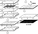
配線基板を治具又は搬送用キャリアにセットする場合は、整合させるためのピンや穴等を使用するなど、任意の公知の位置決め手段を使用して行うことが出来る。例えば図3に示すように、位置セット用ピン冶具6に設けられた基準ピン8と位置決めピン7に、基準穴9と位置決め穴10のあいたサポート板5を通してサポート板5をセット用ピン冶具6と重ね合わせ、更に実装面を下にした基板4の位置決め穴11を通して基板4をそれらと重ね合わせ、更に粘着面を下にした本発明の治具又は搬送用キャリア1の位置決め穴12を通して粘着剤層2の粘着面を基板4の上を向いた裏面にくっつける。次にセット用ピン冶具6のみをはずして、サポート板5、基板4、本発明の治具又は搬送用キャリア1を反転させ、サポート板4を剥がせば配線基板4を冶具1にセットできる。 When the wiring board is set on a jig or a carrier for conveyance, any known positioning means such as a pin or a hole for alignment can be used. For example, as shown in FIG. 3, the support plate 5 and the setting pin jig 6 are inserted into the reference pin 8 and the positioning pin 7 provided in the position setting pin jig 6 through the support plate 5 having the reference hole 9 and the positioning hole 10 therebetween. The substrate 4 is overlapped with the substrate 4 through the positioning holes 11 of the substrate 4 with the mounting surface down, and the adhesive layer through the positioning hole 12 of the jig or carrier 1 of the present invention with the adhesive surface down. The adhesive surface of 2 is attached to the back surface of the substrate 4 facing upward. Next, the wiring board 4 can be set on the jig 1 by removing only the setting pin jig 6 and inverting the support plate 5, the substrate 4, the jig of the present invention or the carrier for conveyance 1 and peeling the support plate 4.
本発明の効果として次が挙げられる。
1.付着防止塗料の存在により、プリントハンダ等に使用するメタルマスクを治具に押し付けてもメタルマスクと治具粘着層とが接触することがなく、くっつきが起こらない。
The following is mentioned as an effect of the present invention.
1. Due to the presence of the anti-adhesion paint, even if a metal mask used for print solder or the like is pressed against the jig, the metal mask does not come into contact with the jig adhesive layer, and sticking does not occur.
2.基板の底面全体を粘着剤により固定する場合には、基板全体が浮き上がり部分を生じることなくしっかりと治具に固定される。粘着性樹脂の粘着性を強くする必要もない。 2. In the case where the entire bottom surface of the substrate is fixed with an adhesive, the entire substrate is firmly fixed to the jig without causing a raised portion. There is no need to increase the adhesiveness of the adhesive resin.
3.粘着性樹脂層を治具の固定用表面全体に存在させることができる。従って、治具上に多数の基板を一度に固定する現実の製作方法では、粘着剤を個々の基板固定のための特定の位置に局在させる面倒な若しくは高度な操作は要求されない。 3. The adhesive resin layer can be present on the entire fixing surface of the jig. Therefore, in an actual manufacturing method in which a large number of substrates are fixed on a jig at once, a troublesome or advanced operation for localizing an adhesive at a specific position for fixing each substrate is not required.
4. 図4に示されるように、粘着剤層を覆う位置決め貫通部を設けた位置決めプレートを冶具の最上層として使用する場合には、配線基板の輪郭が精度を求められずに切断されていると使用できない事態が生じうるが、本発明の冶具又は搬送用キャリアに於いては、付着防止塗料の高さは低いからFPC等の薄く柔軟性のある基板であればそのような輪郭がおおまかな基板であっても、基板貼り付け予定位置と比較した場合の大小にかかわらず、粘着剤に基板底面を付けることができる。 4. As shown in FIG. 4, when a positioning plate provided with a positioning penetrating portion covering the adhesive layer is used as the uppermost layer of the jig, the outline of the wiring board is cut without requiring accuracy. However, in the jig or carrier for transportation of the present invention, the height of the anti-adhesion paint is low, so such a contour is rough if it is a thin and flexible substrate such as an FPC. Even if it is a board | substrate, a board | substrate bottom face can be attached to an adhesive regardless of the magnitude | size when compared with a board | substrate sticking plan position.
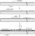
以下図面を参照して本発明を説明する。図1は本発明の治具へ基板を固定する方法の各工程を断面で表すフローチャートである。 The present invention will be described below with reference to the drawings. FIG. 1 is a flowchart showing in cross section each step of a method for fixing a substrate to a jig of the present invention.
治具1の固定用表面には粘着剤層2がある。粘着剤層2の上に、基板4を載せる場所を避けて付着防止塗料3を印刷する。基板4を粘着剤層2の粘着力によって所定位置に固定する。治具1上に基板4が固定された状態で、実装ラインに送られ、プリントハンダなどの工程でメタルマスク6が基板4に押し付けられても、付着防止塗料3が存在するため、メタルマスク6は粘着剤層2に接触しない。 There is an adhesive layer 2 on the fixing surface of the jig 1. On the pressure-sensitive adhesive layer 2, the adhesion preventing paint 3 is printed avoiding the place where the substrate 4 is placed. The substrate 4 is fixed at a predetermined position by the adhesive force of the adhesive layer 2. Even if the substrate 4 is fixed on the jig 1 and sent to the mounting line and the metal mask 6 is pressed against the substrate 4 in a process such as print solder, the metal mask 6 Does not contact the pressure-sensitive adhesive layer 2.
図2は冶具の粘着面で図1の工程を示している。図4は本発明の付着防止塗料3を用いる場合の治具が、トッププレート13を用いる冶具と比較して、基板の輪郭の精度が悪い場合でも対応でき、粘着面と基板の底とが接触出来るという、本発明の利点を示している。 FIG. 2 shows the process of FIG. 1 on the adhesive surface of the jig. FIG. 4 shows that the jig in the case of using the anti-adhesion paint 3 of the present invention can cope with the case where the accuracy of the outline of the substrate is lower than the jig using the top plate 13, and the adhesive surface and the bottom of the substrate are in contact with each other. It shows the advantage of the present invention that it can.
本発明は、治具として、又は運搬用キャリアとして産業上の利用可能性が存在する。治具としては、例えばフレキシブルプリント配線基板に電子部品を半田付けする際に、クリーム半田をメタルマスクを通して基板上にのせる際等に、基板を固定するとき利用すれば有用である。 The present invention has industrial applicability as a jig or as a carrier for transportation. As a jig, for example, when soldering an electronic component to a flexible printed wiring board, it is useful if it is used to fix the board, for example, when cream solder is placed on the board through a metal mask.
1 治具又は搬送キャリア
2 粘着剤層
3 網点状に付けられた付着防止塗料
4 薄い基板
5 クリームハンダ
6 メタルマスク
1 Jig or carrier
2 Adhesive layer
3 Anti-adhesion paint applied in a dot pattern
4 Thin substrate
5 Cream solder
6 Metal mask
Claims (1)
該治具又は搬送用キャリアの固定用表面をべた塗りされた粘着剤層とし、
該治具又は搬送用キャリアの該粘着力ある固定用表面の配線基体を固定する位置以外の位置に、点状に満遍なく分散させて付けるか、又は網目若しくは格子状に付けた付着防止塗料を有していることを特徴とする治具又は搬送用キャリア。 In a jig or carrier for fixing a certain number of wiring bases of one or more by the adhesive force of the fixing surface of the jig or carrier,
With the adhesive layer coated on the surface of the jig or the carrier for fixation,
The jig or the carrier for transportation has a non-adhesive anti-coating paint that is dispersed evenly in a dot pattern or in a mesh or grid pattern at a position other than the position where the wiring substrate on the adhesive fixing surface is fixed. A jig or a carrier for conveyance, characterized in that
Priority Applications (1)
| Application Number | Priority Date | Filing Date | Title |
|---|---|---|---|
| JP2004108307A JP2005294579A (en) | 2004-03-31 | 2004-03-31 | Jig for fixing wiring board on adhesive surface having anti-sticking coating |
Applications Claiming Priority (1)
| Application Number | Priority Date | Filing Date | Title |
|---|---|---|---|
| JP2004108307A JP2005294579A (en) | 2004-03-31 | 2004-03-31 | Jig for fixing wiring board on adhesive surface having anti-sticking coating |
Publications (1)
| Publication Number | Publication Date |
|---|---|
| JP2005294579A true JP2005294579A (en) | 2005-10-20 |
Family
ID=35327165
Family Applications (1)
| Application Number | Title | Priority Date | Filing Date |
|---|---|---|---|
| JP2004108307A Pending JP2005294579A (en) | 2004-03-31 | 2004-03-31 | Jig for fixing wiring board on adhesive surface having anti-sticking coating |
Country Status (1)
| Country | Link |
|---|---|
| JP (1) | JP2005294579A (en) |
Cited By (4)
| Publication number | Priority date | Publication date | Assignee | Title |
|---|---|---|---|---|
| JP2008221539A (en) * | 2007-03-09 | 2008-09-25 | Fuji Mach Mfg Co Ltd | Screen printing device |
| JP2009147353A (en) * | 2009-01-27 | 2009-07-02 | Suzuka Fuji Xerox Co Ltd | Carrier for transporting substrate |
| JP2011077241A (en) * | 2009-09-30 | 2011-04-14 | Suzuka Fuji Xerox Co Ltd | Method of manufacturing transfer carrier |
| CN113724600A (en) * | 2021-09-02 | 2021-11-30 | 业成科技(成都)有限公司 | Manufacturing method of display screen |
-
2004
- 2004-03-31 JP JP2004108307A patent/JP2005294579A/en active Pending
Cited By (4)
| Publication number | Priority date | Publication date | Assignee | Title |
|---|---|---|---|---|
| JP2008221539A (en) * | 2007-03-09 | 2008-09-25 | Fuji Mach Mfg Co Ltd | Screen printing device |
| JP2009147353A (en) * | 2009-01-27 | 2009-07-02 | Suzuka Fuji Xerox Co Ltd | Carrier for transporting substrate |
| JP2011077241A (en) * | 2009-09-30 | 2011-04-14 | Suzuka Fuji Xerox Co Ltd | Method of manufacturing transfer carrier |
| CN113724600A (en) * | 2021-09-02 | 2021-11-30 | 业成科技(成都)有限公司 | Manufacturing method of display screen |
Similar Documents
| Publication | Publication Date | Title |
|---|---|---|
| JP5905718B2 (en) | Conveying jig, conveying method, and conveying jig material | |
| JPWO2006038496A6 (en) | Long film circuit board, manufacturing method thereof and manufacturing apparatus thereof | |
| TW200305235A (en) | Releasing layer transfer film and laminate film | |
| JP2002374062A (en) | Fixation method for flexible printed-circuit board | |
| JP2005294579A (en) | Jig for fixing wiring board on adhesive surface having anti-sticking coating | |
| JP2005072556A (en) | Wiring substrate carrier | |
| JP2005294578A (en) | Jig with adhesive force for fixing wiring board adjusted by adhesive attached in mesh structure or in regularly arranged dot structure | |
| TWI353203B (en) | ||
| JP2002232197A5 (en) | ||
| JP2002232197A (en) | Electronic component mounting method | |
| JP2007266558A (en) | Adhesive sheet, method of manufacturing adhesive sheet, and fixture for wiring board | |
| JP4038517B2 (en) | Flexible printed wiring board for COF and method for manufacturing the same | |
| JP4330465B2 (en) | Method for manufacturing fixture for thin substrate | |
| JP4331047B2 (en) | Manufacturing method of electronic component holder | |
| JP2006210609A (en) | Jig for mounting printed circuit boards | |
| JP4075652B2 (en) | Manufacturing method of semiconductor device | |
| JP4314834B2 (en) | Circuit board manufacturing method and circuit board member | |
| JP2004363438A (en) | Circuit board holding tool | |
| JP2006080212A (en) | Electronic component holder and its manufacturing method | |
| JP2004071803A (en) | Material for circuit board, and production of circuit board | |
| JP2010129940A (en) | Substrate holder for use in soldering | |
| CN104241145A (en) | Method for Producing a Semiconductor Module by Using an Adhesion Carrier | |
| JP2024161627A (en) | Manufacturing method of adhesive holding jig | |
| JP3171894B2 (en) | Adhesive transfer method and electronic component mounting method using the same | |
| JP2007048807A (en) | Jig for holding and transferring flexible substrate, and manufacturing method therefor |
Legal Events
| Date | Code | Title | Description |
|---|---|---|---|
| A072 | Dismissal of procedure |
Free format text: JAPANESE INTERMEDIATE CODE: A073 Effective date: 20060214 |