JP2005294506A - Member for heat treatment - Google Patents
Member for heat treatment Download PDFInfo
- Publication number
- JP2005294506A JP2005294506A JP2004106931A JP2004106931A JP2005294506A JP 2005294506 A JP2005294506 A JP 2005294506A JP 2004106931 A JP2004106931 A JP 2004106931A JP 2004106931 A JP2004106931 A JP 2004106931A JP 2005294506 A JP2005294506 A JP 2005294506A
- Authority
- JP
- Japan
- Prior art keywords
- heat treatment
- film
- sic
- thickness
- hill
- Prior art date
- Legal status (The legal status is an assumption and is not a legal conclusion. Google has not performed a legal analysis and makes no representation as to the accuracy of the status listed.)
- Granted
Links
- 238000010438 heat treatment Methods 0.000 title claims abstract description 33
- 239000011248 coating agent Substances 0.000 claims abstract description 40
- 238000000576 coating method Methods 0.000 claims abstract description 40
- 239000013078 crystal Substances 0.000 claims abstract description 15
- 239000002245 particle Substances 0.000 claims description 39
- 239000000463 material Substances 0.000 claims description 11
- 230000001186 cumulative effect Effects 0.000 abstract description 7
- HBMJWWWQQXIZIP-UHFFFAOYSA-N silicon carbide Chemical compound [Si+]#[C-] HBMJWWWQQXIZIP-UHFFFAOYSA-N 0.000 description 45
- 229910010271 silicon carbide Inorganic materials 0.000 description 45
- 238000000151 deposition Methods 0.000 description 20
- 230000008021 deposition Effects 0.000 description 20
- 238000001000 micrograph Methods 0.000 description 14
- 238000004518 low pressure chemical vapour deposition Methods 0.000 description 11
- 239000000758 substrate Substances 0.000 description 10
- 208000037998 chronic venous disease Diseases 0.000 description 8
- 238000004519 manufacturing process Methods 0.000 description 7
- 230000000052 comparative effect Effects 0.000 description 6
- 230000003746 surface roughness Effects 0.000 description 6
- 229910003902 SiCl 4 Inorganic materials 0.000 description 4
- 238000005229 chemical vapour deposition Methods 0.000 description 3
- 238000004140 cleaning Methods 0.000 description 3
- 239000004065 semiconductor Substances 0.000 description 3
- ATUOYWHBWRKTHZ-UHFFFAOYSA-N Propane Chemical compound CCC ATUOYWHBWRKTHZ-UHFFFAOYSA-N 0.000 description 2
- 238000005137 deposition process Methods 0.000 description 2
- 238000005516 engineering process Methods 0.000 description 2
- 238000000034 method Methods 0.000 description 2
- 239000002994 raw material Substances 0.000 description 2
- VXEGSRKPIUDPQT-UHFFFAOYSA-N 4-[4-(4-methoxyphenyl)piperazin-1-yl]aniline Chemical compound C1=CC(OC)=CC=C1N1CCN(C=2C=CC(N)=CC=2)CC1 VXEGSRKPIUDPQT-UHFFFAOYSA-N 0.000 description 1
- OKTJSMMVPCPJKN-UHFFFAOYSA-N Carbon Chemical compound [C] OKTJSMMVPCPJKN-UHFFFAOYSA-N 0.000 description 1
- UFHFLCQGNIYNRP-UHFFFAOYSA-N Hydrogen Chemical compound [H][H] UFHFLCQGNIYNRP-UHFFFAOYSA-N 0.000 description 1
- 229910052581 Si3N4 Inorganic materials 0.000 description 1
- 239000006061 abrasive grain Substances 0.000 description 1
- 238000009825 accumulation Methods 0.000 description 1
- 229910052799 carbon Inorganic materials 0.000 description 1
- 239000012141 concentrate Substances 0.000 description 1
- 238000001816 cooling Methods 0.000 description 1
- 239000001257 hydrogen Substances 0.000 description 1
- 229910052739 hydrogen Inorganic materials 0.000 description 1
- 238000005470 impregnation Methods 0.000 description 1
- 230000001788 irregular Effects 0.000 description 1
- 238000003754 machining Methods 0.000 description 1
- 239000002184 metal Substances 0.000 description 1
- 229910003465 moissanite Inorganic materials 0.000 description 1
- 239000001294 propane Substances 0.000 description 1
- 238000005488 sandblasting Methods 0.000 description 1
- 229910052710 silicon Inorganic materials 0.000 description 1
- 239000010703 silicon Substances 0.000 description 1
- HQVNEWCFYHHQES-UHFFFAOYSA-N silicon nitride Chemical compound N12[Si]34N5[Si]62N3[Si]51N64 HQVNEWCFYHHQES-UHFFFAOYSA-N 0.000 description 1
- 239000005049 silicon tetrachloride Substances 0.000 description 1
Images


Abstract
Description
本発明は、半導体製造プロセスのうち加熱を伴う工程で使用される熱処理用部材に関する。 The present invention relates to a heat treatment member used in a process involving heating in a semiconductor manufacturing process.
半導体製造プロセスのうちで加熱を伴う工程、例えば、LP−CVD(Low Pressure-Chemical Vapor Deposition:低圧CVD)によるSi3N4(窒化ケイ素)膜デポ工程においては、基材表面が多結晶のSiC(炭化ケイ素)によりコーティングされている熱処理用部材が用いられている。 In a process involving heating in a semiconductor manufacturing process, for example, a Si 3 N 4 (silicon nitride) film deposition process by LP-CVD (Low Pressure-Chemical Vapor Deposition), the substrate surface is made of polycrystalline SiC. A heat treatment member coated with (silicon carbide) is used.
従来、この種の熱処理用部材としては、ウェーハと接触する面や高い精度が求められる箇所に機械加工を施して極めて凹凸の少ない面とした基材表面が多結晶のSiCによりコーティングされているもの、あるいは凹凸加工を施した基材表面が多結晶のSiCによりコーティングされているものが知られている。 Conventionally, as this type of heat treatment member, the surface of the substrate that has been subjected to machining on the surface that comes into contact with the wafer and where high accuracy is required to have a very uneven surface is coated with polycrystalline SiC. Alternatively, it is known that the surface of a base material subjected to uneven processing is coated with polycrystalline SiC.
しかし、従来の熱処理用部材では、半導体ウェーハへのLP−CVDによるSi3N4膜デポ工程に使用する際、基材表面が平滑な前者の場合、冷熱サイクルによりSi3N4デポ膜に多結晶のSiC膜との熱膨張係数の違いによって引張応力が発生し、堆積するSi3N4デポ膜の累積膜厚が小さいうちにクラックが発生してその剥がれやずれによるダストが半導体デバイスの歩留まりを低下させてしまう不具合がある。
かかる不具合に対処するため、デバイスメーカーでは、熱処理用部材のデポ膜除去洗浄タイミングを早めて使用しているため、製造装置の実稼働時間が比較的短い。
However, when the conventional heat treatment member is used in the deposition process of Si 3 N 4 film by LP-CVD on a semiconductor wafer, in the former case where the surface of the substrate is smooth, the Si 3 N 4 deposition film is often formed by a cooling cycle. Tensile stress is generated due to the difference in thermal expansion coefficient from the crystalline SiC film, and cracks occur while the accumulated film thickness of the deposited Si 3 N 4 deposition film is small. There is a problem that lowers.
In order to cope with such a problem, since the device manufacturer uses the deposition film removal cleaning timing of the heat treatment member in advance, the actual operation time of the manufacturing apparatus is relatively short.
一方、基材表面が凹凸である後者では、前者よりデポ膜除去洗浄タイミングを幾分遅くはできるものの、炉内パーティクルの突発により、堆積するSi3N4デポ膜の累積膜厚を9μmを超えて大きくすることは困難である。
かような炉内パーティクルの突発は、Si3N4デポ膜の累積膜厚が9μmを超えた際に、基材表面の凸部又は凹部と対応する部分のデポ膜に大きなクラックが発生し、パーティクルが非常に多くなるものである。
Such a burst of in-furnace particles, when the cumulative film thickness of the Si 3 N 4 deposition film exceeds 9 μm, a large crack occurs in the deposition film in the part corresponding to the convex part or concave part of the substrate surface, Particles are very many.
本発明は、堆積するデポ膜の累積膜厚を格段に大きくし得る熱処理用部材の提供を課題とする。 It is an object of the present invention to provide a heat treatment member that can significantly increase the accumulated film thickness of the deposited deposition film.
本発明の熱処理用部材は、基材表面が多結晶のSiCによりコーティングされている熱処理用部材であって、コーティング表面が基部の最大直径20〜100μm、1mm2当たり150〜3500個の密度で存在する丘状凸部により凹凸形状をなすように設けられていることを特徴とする。 The heat treatment member of the present invention is a heat treatment member whose base material surface is coated with polycrystalline SiC, and the coating surface has a maximum diameter of 20 to 100 μm at the base and a density of 150 to 3500 per mm 2 It is provided so that it may be uneven | corrugated by the hill-shaped convex part to make.
一方、前記コーティング膜を形成するSiC単結晶粒子が最大粒径2〜10μmであることが好ましい。 On the other hand, it is preferable that the SiC single crystal particles forming the coating film have a maximum particle size of 2 to 10 μm.
又、前記コーティング膜の厚さが30〜100μmであることが好ましい。 Moreover, it is preferable that the thickness of the said coating film is 30-100 micrometers.
本発明の熱処理用部材によれば、堆積するデポ膜の各部に発生する応力が均等に分散されるので、デポ膜の累積膜厚を格段に大きくすることができ、ひいては熱処理用部材のデポ膜除去洗浄に要する時間を低減することができる。 According to the heat treatment member of the present invention, the stress generated in each portion of the deposited deposition film is evenly distributed, so that the accumulated film thickness of the deposition film can be remarkably increased. The time required for removal cleaning can be reduced.
一方、コーティング膜を形成するSiC単結晶粒子が最大粒径2〜10μmであることにより、SiC単結晶粒子と対応する部分のデポ膜に発生する応力が集中することがないので、デポ膜の累積膜厚をより一層大きくすることができる。 On the other hand, since the SiC single crystal particles forming the coating film have a maximum particle size of 2 to 10 μm, the stress generated in the deposition film corresponding to the SiC single crystal particles does not concentrate, so the accumulation of the deposition film The film thickness can be further increased.
基材としては、Si含浸SiC焼結体(反応焼結SiC)、自焼結SiC、カーボン、その他が用いられる。
基材表面は、平滑であっても、凹凸であってもよいが、凹凸である場合、凸部の大きさは、丘状凸部の大きさの同等以下とする。
As the substrate, Si-impregnated SiC sintered body (reaction sintered SiC), self-sintered SiC, carbon, or the like is used.
The surface of the substrate may be smooth or uneven, but in the case of unevenness, the size of the convex portion is equal to or less than the size of the hill-shaped convex portion.
丘状凸部は、円錐状の多結晶SiCの表面部であって、ほぼ半球状を呈するものであり、その基部の最大直径が、20μm未満であると、許容される累積膜厚は従来技術並(<15μm)である。一方、100μmを超えると、許容される累積膜厚は15〜20μmが上限となる。
丘状凸部の基部の最大直径は、40〜70μmがより好ましい。
ここで、基部とは、丘状凸部の裾をいう。
The hill-shaped convex portion is a surface portion of conical polycrystalline SiC and has a substantially hemispherical shape. If the maximum diameter of the base portion is less than 20 μm, the allowable cumulative film thickness is the conventional technology. Average (<15 μm). On the other hand, if it exceeds 100 μm, the upper limit of the allowable accumulated film thickness is 15 to 20 μm.
As for the maximum diameter of the base part of a hill-shaped convex part, 40-70 micrometers is more preferable.
Here, the base portion refers to the skirt of the hill-shaped convex portion.
丘状凸部の1mm2当たりに存在する密度が、150個未満であると、許容される累積膜厚は従来技術並(<15μm)となる。一方、3500個を超えても許容される累積膜厚は従来技術並(<15μm)となる。
丘状凸部の1mm2当たりに存在する密度は、400〜2000個がより好ましい。
When the density existing per 1 mm 2 of the hill-shaped convex portions is less than 150, the allowable accumulated film thickness is equivalent to the conventional technology (<15 μm). On the other hand, even if the number exceeds 3,500, the allowable accumulated film thickness is the same as that in the prior art (<15 μm).
Density present in 1 mm 2 per hill shaped convex part, 400 to 2,000 pieces is more preferred.
一方、コーティング膜を形成するSiC単結晶粒子の最大粒径が、2μm未満であると、許容される累積膜厚を飛躍的に大きくすることは難しい。一方、10μmを超えると、突発的にパーティクル量が増えることがある。
コーティング膜を形成するSiC単結晶粒子の最大直径は、7〜9μmがより好ましい。
On the other hand, if the maximum particle size of the SiC single crystal particles forming the coating film is less than 2 μm, it is difficult to dramatically increase the allowable accumulated film thickness. On the other hand, if it exceeds 10 μm, the amount of particles may suddenly increase.
As for the maximum diameter of the SiC single crystal particle which forms a coating film, 7-9 micrometers is more preferable.
又、コーティング膜の厚さが、30μm未満であると、CVDSiC膜の特性が長続きしない。一方、100μmを超えても性能は更に向上することがない。
コーティング膜の厚さは、30〜80μmがより好ましい。
ここで、コーティング膜の厚さとは、基材表面が平滑な場合、(コーティング膜の凹部の厚さ+コーティング膜の凸部の厚さ)÷2をいい、基材表面に凹凸がある場合、(断面の最大厚さ+断面の最小厚さ)÷2をいう。
If the thickness of the coating film is less than 30 μm, the characteristics of the CVD SiC film do not last long. On the other hand, even if it exceeds 100 μm, the performance is not further improved.
As for the thickness of a coating film, 30-80 micrometers is more preferable.
Here, the thickness of the coating film refers to (the thickness of the concave portion of the coating film + the thickness of the convex portion of the coating film) / 2 when the surface of the base material is smooth. (Maximum thickness of the cross section + Minimum thickness of the cross section) ÷ 2.
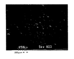
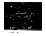
図1、図2及び図3は、それぞれ本発明に係る熱処理用部材の実施例1を示す表面の粒子構造の顕微鏡写真、図1の部分拡大顕微鏡写真及び図2の部分拡大顕微鏡写真である。 1, FIG. 2 and FIG. 3 are a micrograph of the particle structure of the surface showing Example 1 of the member for heat treatment according to the present invention, a partially magnified micrograph of FIG. 1, and a partially magnified micrograph of FIG.
この熱処理用部材は、表面粗さRaを0.1μm程度に表面を平滑にしたSi(金属シリコン)含浸SiC焼結体を基材とし、その表面が多結晶のSiCによりコーティングされているものである。
そして、コーティング表面が、前記基部の最大直径20〜100μm、1mm2当たり150〜3500個の密度(n=10での範囲、以下同じ)で存在するほぼ半球状の丘状凸部により凹凸形状をなすように設けられており、コーティング膜を形成するSiC単結晶粒子の最大粒径が2〜10μmであり、又、コーティング膜の厚さ((凹部の厚さ+凸部の厚さ)÷2)が50〜60μmであるものである。
This heat treatment member is made of a Si (metal silicon) -impregnated SiC sintered body whose surface roughness Ra is about 0.1 μm and whose surface is coated with polycrystalline SiC. is there.
The coating surface has an uneven shape due to a substantially hemispherical hill-shaped convex portion having a maximum diameter of 20 to 100 μm of the base and a density of 150 to 3500 per 1 mm 2 (range at n = 10, hereinafter the same). The maximum particle size of the SiC single crystal particles forming the coating film is 2 to 10 μm, and the thickness of the coating film ((thickness of the concave portion + thickness of the convex portion) / 2 ) Is 50 to 60 μm.
上述した熱処理用部材を製造するには、先ず、SiC仮焼体をSiと反応焼結させた後に、研削加工を施して表面が表面粗さRaが0.1μm程度の平滑なSi含浸SiC焼結体を基材とする。
次に、基材表面にCVD法により多結晶のSiCをコーティングするのであるが、CVD初期段階において、原料供給濃度を大きく(対キャリアーモル比で1.5〜5倍と)し、コーティング表面が、基部の最大直径20〜90μm、1mm2当たり200〜10000個の密度で存在するほぼ半球状の丘状凸部により凹凸形状をなすようにした後、定常の原料供給濃度に戻してCVDし、最終的なコーティング表面が、基部の最大直径20〜100μm、1mm2当たり150〜3500個の密度で存在するほぼ半球状の丘状凸部により凹凸形状をなすと共に、コーティング膜を形成するSiC単結晶粒子の最大粒径が2〜10μmであり、かつ、コーティング膜の厚さが30〜100μmであるようにする。
なお、CVD条件は、以下の通りである。
温度:1200℃
ガス(定常):SiCl4(四塩化ケイ素)+C3H8(プロパン)+H2(水素)=3+1+20slm
In order to manufacture the above-mentioned heat treatment member, first, the SiC calcined body is reacted and sintered with Si, and then subjected to grinding to obtain a smooth Si-impregnated SiC sintered body having a surface roughness Ra of about 0.1 μm. The bonded body is used as a base material.
Next, the surface of the substrate is coated with polycrystalline SiC by CVD. In the initial stage of CVD, the raw material supply concentration is increased (1.5 to 5 times the carrier molar ratio), and the coating surface is The base has a maximum diameter of 20 to 90 μm, and an irregular shape is formed by a substantially hemispherical hill-shaped convex portion present at a density of 200 to 10,000 per 1 mm 2 , and then the CVD is performed by returning to a steady raw material supply concentration. The SiC single crystal that forms a coating film while the final coating surface has an uneven shape due to a substantially hemispherical hill-shaped convex portion having a maximum diameter of 20 to 100 μm at the base and a density of 150 to 3500 per mm 2 The maximum particle size of the particles is 2 to 10 μm, and the thickness of the coating film is 30 to 100 μm.
The CVD conditions are as follows.
Temperature: 1200 ° C
Gas (stationary): SiCl 4 (silicon tetrachloride) + C 3 H 8 (propane) + H 2 (hydrogen) = 3 + 1 + 20 slm
ここで、上述した熱処理用部材を用いて、LP−CVDによるSi3N4膜デポ工程を行ったところ、Si3N4デポ膜の許容累積膜厚は、表1に示すように、20μm以上となり、又、LP−CVDの炉内におけるSi3N4パーティクル量は、表1に示すように、少なかった。 Here, when the Si 3 N 4 film deposition step by LP-CVD was performed using the heat treatment member described above, the allowable cumulative film thickness of the Si 3 N 4 deposition film was 20 μm or more as shown in Table 1. As shown in Table 1, the amount of Si 3 N 4 particles in the LP-CVD furnace was small.

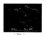
図4及び図5は、それぞれ本発明に係る熱処理用部材の実施例2を示す表面の粒子構造の顕微鏡写真及び図4の部分拡大顕微鏡写真である。 4 and 5 are a micrograph of a particle structure on the surface and a partially enlarged micrograph of FIG. 4, respectively, showing Example 2 of the member for heat treatment according to the present invention.
この熱処理用部材は、前記基部の最大直径10〜100μm、1mm2当たり100〜1000個の密度で存在する丘状凸部により表面が凹凸形状をなすように設けられたSi含浸SiC焼結体を基材とし、その表面が多結晶のSiCによりコーティングされているものである。
そして、コーティング表面が、基部の最大直径70〜80μm、1mm2当たり200〜1000個の密度で存在するほぼ半球状の丘状凸部により凹凸形状をなすように設けられており、コーティング膜を形成するSiC単結晶粒子の最大粒径が9〜10μmであり、又、コーティング膜の厚さ(断面の最大厚さ+断面の最小厚さ)が、40〜50μmであるものである。
This heat-treating member is a Si-impregnated SiC sintered body provided such that the surface has a concavo-convex shape by hill-shaped convex portions having a maximum diameter of 10 to 100 μm of the base and a density of 100 to 1000 per 1 mm 2. The substrate is a substrate whose surface is coated with polycrystalline SiC.
And the coating surface is provided so as to form an uneven shape by a substantially hemispherical hill-shaped convex portion having a maximum diameter of 70 to 80 μm at the base and a density of 200 to 1000 per 1 mm 2 to form a coating film The maximum grain size of the SiC single crystal particles is 9 to 10 μm, and the thickness of the coating film (the maximum thickness of the cross section + the minimum thickness of the cross section) is 40 to 50 μm.
上述した熱処理用部材を製造するには、先ず、SiC仮焼体にSiを含浸した後、染み出したSiをグラインダーで除去し、しかる後に、その表面を、#1800のSiC砥粒を用い、1kgf/cm2の圧力で全面サンドブラスト処理し、表面が、基部の最大直径10〜100μm、1mm2当たり100〜1000個の密度で存在するほぼ半球状の丘状凸部により凹凸形状をなすSi含浸SiC焼結体を基材とする。
次に、基材表面にCVD法により多結晶のSiCをコーティングし、コーティング表面が、基部の最大直径20〜100μm、1mm2当たり200〜2500個の密度で存在するほぼ半球状の丘状凸部により凹凸形状をなすと共に、コーティング膜を形成するSiC単結晶粒子の最大粒径が2〜10μmで、かつ、コーティング膜の厚さが30〜100μmであるようにする。
なお、CVD条件は、以下の通りである。
温度:1250℃
ガス:SiCl4+C3H8+H2=3+1+20slm
To manufacture the above-mentioned heat treatment member, first, after impregnating the SiC calcined body with Si, the exuded Si was removed with a grinder, and then the surface was used with # 1800 SiC abrasive grains. Si impregnation is performed by sandblasting the entire surface at a pressure of 1 kgf / cm 2 , and the surface is formed into an uneven shape by a substantially hemispherical hill-shaped convex portion having a maximum diameter of 10 to 100 μm at the base and a density of 100 to 1000 per mm 2 A SiC sintered body is used as a base material.
Next, the surface of the base material is coated with polycrystalline SiC by a CVD method, and the coating surface has a maximum hemispherical hill-shaped convex portion having a maximum diameter of 20 to 100 μm and a density of 200 to 2500 per mm 2. The SiC single crystal particles forming the coating film have a maximum particle diameter of 2 to 10 μm, and the coating film thickness is 30 to 100 μm.
The CVD conditions are as follows.
Temperature: 1250 ° C
Gas: SiCl 4 + C 3 H 8 + H 2 = 3 + 1 + 20 slm
ここで、上述した熱処理用部材を用いて、LP−CVDによるSi3N4膜デポ工程を行ったところ、Si3N4デポ膜の許容累積膜厚は、表1に示すように、20μmを超え、又、LP−CVDの炉内におけるSi3N4パーティクル量は、表1に示すように、少なかった。
(比較例1)
Here, when the Si 3 N 4 film deposition step by LP-CVD was performed using the heat treatment member described above, the allowable accumulated film thickness of the Si 3 N 4 deposition film was 20 μm as shown in Table 1. Further, as shown in Table 1, the amount of Si 3 N 4 particles in the LP-CVD furnace was small.
(Comparative Example 1)
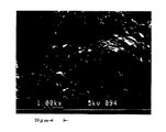
図6及び図7は、比較のための熱処理用部材の比較例1を示す表面の粒子構造の顕微鏡写真及び図6の部分拡大顕微鏡写真である。 6 and 7 are a micrograph of a particle structure on the surface and a partially enlarged micrograph of FIG. 6 showing Comparative Example 1 of a heat treatment member for comparison.
この熱処理用部材は、表面粗さRaが0.1μm程度に表面を平滑にしたSi含浸SiC焼結体を基材とし、その表面が多結晶のSiCによりコーティングされているものである。
そして、コーティング表面が、基部の最大直径90〜140μm、1mm2当たり2〜5個の密度で存在するほぼ半球状の丘状凸部によりまばらな凸形状をなすように設けられており、コーティング膜を形成するSiC単結晶粒子の最大粒径が1〜5μmであり、又、コーティング膜の厚さ(丘状凸部を除く部分の厚さ)が、40〜60μmであるものである。
This heat treatment member uses a Si-impregnated SiC sintered body having a surface roughness Ra of about 0.1 μm as a base, and the surface thereof is coated with polycrystalline SiC.
The coating surface is provided so as to form a sparse convex shape by a substantially hemispherical hill-shaped convex portion having a maximum diameter of 90 to 140 μm at the base and a density of 2 to 5 per 1 mm 2 , and a coating film The maximum particle size of the SiC single crystal particles forming the film is 1 to 5 μm, and the thickness of the coating film (the thickness of the portion excluding the hill-shaped convex portion) is 40 to 60 μm.
上述した熱処理用部材を製造するには、先ず、実施例1と同様に、SiC仮焼体にSiを含浸した後、染み出したSiをグラインダーで除去し、しかる後に、研削加工を施して表面が表面粗さRaが0.1μm程度の平滑なSi含浸SiC焼結体を基材とする。
次に、基材表面にCVD法により多結晶のSiCをコーティングし、コーティング表面が、基部の最大直径90〜140μm、1mm2当たり50〜130個の密度で存在するほぼ半球状の丘状凸部によりまばらな凸形状をなすと共に、コーティング膜を形成するSiC単結晶粒子の最大粒径が15〜20μmで、かつ、丘状凸部の部分を除くコーティング膜の厚さが60〜70μmであるようにする。
なお、CVD条件は、以下の通りである。
温度:1250℃
ガス:SiCl4+C3H8+H2=3+1+20slm
In order to manufacture the above-described heat treatment member, first, as in Example 1, after the SiC calcined body was impregnated with Si, the exuded Si was removed with a grinder, and then grinding was applied to the surface. The base material is a smooth Si-impregnated SiC sintered body having a surface roughness Ra of about 0.1 μm.
Next, the surface of the base material is coated with polycrystalline SiC by the CVD method, and the coating surface has a maximum hemispherical hill-shaped convex portion having a maximum diameter of 90 to 140 μm and a density of 50 to 130 per mm 2. The maximum grain size of the SiC single crystal particles forming the coating film is 15 to 20 μm, and the thickness of the coating film excluding the hill-shaped convex part is 60 to 70 μm. To.
The CVD conditions are as follows.
Temperature: 1250 ° C
Gas: SiCl 4 + C 3 H 8 + H 2 = 3 + 1 + 20 slm
ここで、上述した熱処理用部材を用いて、LP−CVDによるSi3N4膜デポ工程を行ったところ、Si3N4デポ膜の許容累積膜厚は、表1に示すように、15〜20μmとなり、又、LP−CVDの炉内におけるSi3N4パーティクル量は、表1に示すように、少なかった。
(比較例2)
Here, when the Si 3 N 4 film deposition step by LP-CVD was performed using the heat treatment member described above, the allowable cumulative film thickness of the Si 3 N 4 deposition film was 15 to 15 as shown in Table 1. As shown in Table 1, the amount of Si 3 N 4 particles in the LP-CVD furnace was small.
(Comparative Example 2)
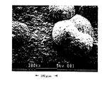
図8及び図9は、比較のための熱処理用部材の比較例2を示す表面の粒子構造の顕微鏡写真及び図8の部分拡大顕微鏡写真である。 8 and 9 are a micrograph of a particle structure on the surface and a partially enlarged micrograph of FIG. 8 showing Comparative Example 2 of a heat treatment member for comparison.
この熱処理用部材は、表面粗さRaが0.1μm程度に表面を平滑にしたSi含浸SiC焼結体を基材とし、その表面が多結晶のSiCによりコーティングされているものである。
そして、コーティング表面が、基部の最大直径10〜20μm、1mm2当たり50〜120個の密度で存在するほぼ半球状の丘状凸部により凹凸形状をなすように設けられており、コーティング膜を形成するSiC単結晶粒子の最大粒径が8〜20μmであり、又、コーティング膜の厚さ((凹部の厚さ+凸部の厚さ)÷2)が50〜60μmであるものである。
This heat treatment member uses a Si-impregnated SiC sintered body having a surface roughness Ra of about 0.1 μm as a base, and the surface thereof is coated with polycrystalline SiC.
And the coating surface is provided so as to form an uneven shape by a substantially hemispherical hill-shaped convex portion having a maximum diameter of 10 to 20 μm at the base and a density of 50 to 120 per 1 mm 2 , thereby forming a coating film The maximum particle diameter of the SiC single crystal particles to be formed is 8 to 20 μm, and the thickness of the coating film ((thickness of the concave portion + thickness of the convex portion) / 2) is 50 to 60 μm.
上述した熱処理用部材を製造するには、先ず、実施例1と同様に、SiC仮焼体にSiを含浸した後、染み出したSiをグラインダーで除去し、しかる後に、研削加工を施して表面が表面粗さRaが0.1μm程度の平滑なSi含浸SiC焼結体を基材とする。
次に、基材表面にCVD法により多結晶のSiCをコーティングし、コーティング表面が、基部の最大直径10〜20μm、1mm2当たり3500〜12000個の密度で存在するほぼ半球状の丘状凸部により凹凸形状をなすと共に、コーティング膜を形成するSiC単結晶粒子の最大直径が8〜20μmであり、かつ、コーティング膜の厚さが40〜50μmであるようにする。
なお、CVD条件は、以下の通りである。
温度:1200℃
ガス:SiCl4+C3H8+H2=3+1.1+20slm
In order to manufacture the above-described heat treatment member, first, as in Example 1, after the SiC calcined body was impregnated with Si, the exuded Si was removed with a grinder, and then grinding was applied to the surface. The base material is a smooth Si-impregnated SiC sintered body having a surface roughness Ra of about 0.1 μm.
Next, the surface of the base material is coated with polycrystalline SiC by a CVD method, and the coating surface has a maximum hemispherical hill-shaped convex portion having a maximum diameter of 10 to 20 μm and a density of 3500 to 12000 per mm 2. The SiC single crystal particles forming the coating film have a maximum diameter of 8 to 20 μm, and the thickness of the coating film is 40 to 50 μm.
The CVD conditions are as follows.
Temperature: 1200 ° C
Gas: SiCl 4 + C 3 H 8 + H 2 = 3 + 1.1 + 20 slm
ここで、上述した熱処理用部材を用いて、LP−CVDによるSi3N4膜デポ工程を行ったところ、Si3N4デポ膜の許容累積膜厚は、表1に示すように、15μm未満となり、又、LP−CVDの炉内におけるSi3N4パーティクル量は、表1に示すように、多かった。 Here, when the Si 3 N 4 film deposition step by LP-CVD was performed using the heat treatment member described above, the allowable cumulative film thickness of the Si 3 N 4 deposition film was less than 15 μm as shown in Table 1. As shown in Table 1, the amount of Si 3 N 4 particles in the LP-CVD furnace was large.
Claims (3)
The heat-treating member according to claim 1 or 2, wherein the coating film has a thickness of 30 to 100 µm.
Priority Applications (1)
| Application Number | Priority Date | Filing Date | Title |
|---|---|---|---|
| JP2004106931A JP4255019B2 (en) | 2004-03-31 | 2004-03-31 | Material for heat treatment |
Applications Claiming Priority (1)
| Application Number | Priority Date | Filing Date | Title |
|---|---|---|---|
| JP2004106931A JP4255019B2 (en) | 2004-03-31 | 2004-03-31 | Material for heat treatment |
Publications (2)
| Publication Number | Publication Date |
|---|---|
| JP2005294506A true JP2005294506A (en) | 2005-10-20 |
| JP4255019B2 JP4255019B2 (en) | 2009-04-15 |
Family
ID=35327105
Family Applications (1)
| Application Number | Title | Priority Date | Filing Date |
|---|---|---|---|
| JP2004106931A Expired - Lifetime JP4255019B2 (en) | 2004-03-31 | 2004-03-31 | Material for heat treatment |
Country Status (1)
| Country | Link |
|---|---|
| JP (1) | JP4255019B2 (en) |
Cited By (1)
| Publication number | Priority date | Publication date | Assignee | Title |
|---|---|---|---|---|
| JP2016204737A (en) * | 2015-04-28 | 2016-12-08 | イビデン株式会社 | Ceramic structure and method for manufacturing ceramic structure |
-
2004
- 2004-03-31 JP JP2004106931A patent/JP4255019B2/en not_active Expired - Lifetime
Cited By (1)
| Publication number | Priority date | Publication date | Assignee | Title |
|---|---|---|---|---|
| JP2016204737A (en) * | 2015-04-28 | 2016-12-08 | イビデン株式会社 | Ceramic structure and method for manufacturing ceramic structure |
Also Published As
| Publication number | Publication date |
|---|---|
| JP4255019B2 (en) | 2009-04-15 |
Similar Documents
| Publication | Publication Date | Title |
|---|---|---|
| JP5024382B2 (en) | Susceptor and silicon epitaxial wafer manufacturing method | |
| JP5051909B2 (en) | Vertical wafer boat | |
| JP5063797B2 (en) | Adsorption member, adsorption device, and adsorption method | |
| KR102046811B1 (en) | Epitaxial growth device, method of manufacturing epitaxial wafer, and lift pin for epitaxial growth device | |
| JPH0758041A (en) | Susceptor | |
| JP4782744B2 (en) | Adsorption member, adsorption device, and adsorption method | |
| JP2006086534A (en) | Rough side susceptor for high-temperature substrate processing | |
| WO2004009515A1 (en) | Carbon composite material | |
| JP6219238B2 (en) | Susceptor and manufacturing method thereof | |
| JPH08188468A (en) | Formed silicon carbide produced by chemical vapor deposition and its production | |
| JPH08188408A (en) | Silicon carbide molded product by chemical vapor deposition and its production | |
| JP2008174841A (en) | Susceptor for vapor deposition, and method for producing the same | |
| JP2004200436A (en) | Susceptor and its manufacturing method | |
| JP4255019B2 (en) | Material for heat treatment | |
| JP3811540B2 (en) | Method for producing silicon carbide molded body | |
| JPWO2018207942A1 (en) | Susceptor, method for manufacturing epitaxial substrate, and epitaxial substrate | |
| JP2011100844A (en) | Device having electrostatic chucking function and method of manufacturing the same | |
| JP6460659B2 (en) | Ceramic material | |
| JP6451508B2 (en) | Epitaxial growth apparatus, epitaxial wafer manufacturing method, and lift pin for epitaxial growth apparatus | |
| JP2008007350A (en) | Yttria ceramic sintered compact | |
| JP4619036B2 (en) | Carbon composite material | |
| JP5087375B2 (en) | Method for manufacturing silicon carbide semiconductor device | |
| JP2018104737A (en) | Method of manufacturing vertical wafer boat | |
| US20230026485A1 (en) | Diamond Structures For Tooling | |
| JP7413768B2 (en) | Method for manufacturing polycrystalline substrate |
Legal Events
| Date | Code | Title | Description |
|---|---|---|---|
| A621 | Written request for application examination |
Free format text: JAPANESE INTERMEDIATE CODE: A621 Effective date: 20060907 |
|
| A711 | Notification of change in applicant |
Free format text: JAPANESE INTERMEDIATE CODE: A712 Effective date: 20070711 |
|
| A977 | Report on retrieval |
Free format text: JAPANESE INTERMEDIATE CODE: A971007 Effective date: 20081031 |
|
| A131 | Notification of reasons for refusal |
Free format text: JAPANESE INTERMEDIATE CODE: A131 Effective date: 20081105 |
|
| A521 | Request for written amendment filed |
Free format text: JAPANESE INTERMEDIATE CODE: A523 Effective date: 20081225 |
|
| TRDD | Decision of grant or rejection written | ||
| A01 | Written decision to grant a patent or to grant a registration (utility model) |
Free format text: JAPANESE INTERMEDIATE CODE: A01 Effective date: 20090122 |
|
| A01 | Written decision to grant a patent or to grant a registration (utility model) |
Free format text: JAPANESE INTERMEDIATE CODE: A01 |
|
| A61 | First payment of annual fees (during grant procedure) |
Free format text: JAPANESE INTERMEDIATE CODE: A61 Effective date: 20090122 |
|
| FPAY | Renewal fee payment (event date is renewal date of database) |
Free format text: PAYMENT UNTIL: 20120206 Year of fee payment: 3 |
|
| R150 | Certificate of patent or registration of utility model |
Ref document number: 4255019 Country of ref document: JP Free format text: JAPANESE INTERMEDIATE CODE: R150 Free format text: JAPANESE INTERMEDIATE CODE: R150 |
|
| FPAY | Renewal fee payment (event date is renewal date of database) |
Free format text: PAYMENT UNTIL: 20120206 Year of fee payment: 3 |
|
| FPAY | Renewal fee payment (event date is renewal date of database) |
Free format text: PAYMENT UNTIL: 20130206 Year of fee payment: 4 |
|
| R250 | Receipt of annual fees |
Free format text: JAPANESE INTERMEDIATE CODE: R250 |
|
| FPAY | Renewal fee payment (event date is renewal date of database) |
Free format text: PAYMENT UNTIL: 20140206 Year of fee payment: 5 |
|
| R250 | Receipt of annual fees |
Free format text: JAPANESE INTERMEDIATE CODE: R250 |
|
| R250 | Receipt of annual fees |
Free format text: JAPANESE INTERMEDIATE CODE: R250 |
|
| R250 | Receipt of annual fees |
Free format text: JAPANESE INTERMEDIATE CODE: R250 |
|
| S531 | Written request for registration of change of domicile |
Free format text: JAPANESE INTERMEDIATE CODE: R313531 |
|
| S533 | Written request for registration of change of name |
Free format text: JAPANESE INTERMEDIATE CODE: R313533 |
|
| R350 | Written notification of registration of transfer |
Free format text: JAPANESE INTERMEDIATE CODE: R350 |
|
| R250 | Receipt of annual fees |
Free format text: JAPANESE INTERMEDIATE CODE: R250 |
|
| R250 | Receipt of annual fees |
Free format text: JAPANESE INTERMEDIATE CODE: R250 |
|
| R250 | Receipt of annual fees |
Free format text: JAPANESE INTERMEDIATE CODE: R250 |
|
| R250 | Receipt of annual fees |
Free format text: JAPANESE INTERMEDIATE CODE: R250 |
|
| R250 | Receipt of annual fees |
Free format text: JAPANESE INTERMEDIATE CODE: R250 |
|
| R250 | Receipt of annual fees |
Free format text: JAPANESE INTERMEDIATE CODE: R250 |
|
| R250 | Receipt of annual fees |
Free format text: JAPANESE INTERMEDIATE CODE: R250 |
|
| R250 | Receipt of annual fees |
Free format text: JAPANESE INTERMEDIATE CODE: R250 |
|
| S533 | Written request for registration of change of name |
Free format text: JAPANESE INTERMEDIATE CODE: R313533 |
|
| R350 | Written notification of registration of transfer |
Free format text: JAPANESE INTERMEDIATE CODE: R350 |