JP2005294482A - Electronic component and electronic device - Google Patents
Electronic component and electronic device Download PDFInfo
- Publication number
- JP2005294482A JP2005294482A JP2004106614A JP2004106614A JP2005294482A JP 2005294482 A JP2005294482 A JP 2005294482A JP 2004106614 A JP2004106614 A JP 2004106614A JP 2004106614 A JP2004106614 A JP 2004106614A JP 2005294482 A JP2005294482 A JP 2005294482A
- Authority
- JP
- Japan
- Prior art keywords
- solder bump
- conductive
- convex portion
- solder
- substrate
- Prior art date
- Legal status (The legal status is an assumption and is not a legal conclusion. Google has not performed a legal analysis and makes no representation as to the accuracy of the status listed.)
- Pending
Links
Images


Classifications
-
- H—ELECTRICITY
- H10—SEMICONDUCTOR DEVICES; ELECTRIC SOLID-STATE DEVICES NOT OTHERWISE PROVIDED FOR
- H10W—GENERIC PACKAGES, INTERCONNECTIONS, CONNECTORS OR OTHER CONSTRUCTIONAL DETAILS OF DEVICES COVERED BY CLASS H10
- H10W72/00—Interconnections or connectors in packages
- H10W72/01—Manufacture or treatment
- H10W72/012—Manufacture or treatment of bump connectors, dummy bumps or thermal bumps
Landscapes
- Wire Bonding (AREA)
Abstract
【課題】 半田バンプの強度向上を図ることにより、半田バンプのくびれ部におけるクラックの発生を抑制し、かつ、クラックが発生しても断線不良を起こさず、半田バンプの破壊を防止できる電子部品及び電子装置の提供する。
【解決手段】 本発明に係る電子部品は、第一基板と第二基板が対向して配置され、第一基板の絶縁性を有する一面(第一絶縁部10)側に配された複数個の第一導電部11aと、第二基板の電気絶縁性を有する一面(第三絶縁部30)側に配された複数個の第二導電部32との間に、個別に半田バンプ13を設けてなる。少なくとも1つの半田バンプにおいては、第一導電部11aにおいて半田バンプ13と接する側の一面は、絶縁層(第二絶縁部)12で被覆された外周部と、第一導電部11aと接して配される凸部14を備えた内周部とから構成され、凸部は半田バンプより大きな強度をもつ部材からなる。
【選択図】 図2
PROBLEM TO BE SOLVED: To suppress the occurrence of a crack in a constricted portion of a solder bump by improving the strength of the solder bump, and to prevent the breakage of the solder bump without causing a disconnection defect even if the crack occurs. Provided by electronic device.
In an electronic component according to the present invention, a first substrate and a second substrate are arranged to face each other, and a plurality of layers disposed on one surface (first insulating portion 10) side having insulation properties of the first substrate. Solder bumps 13 are individually provided between the first conductive portion 11a and the plurality of second conductive portions 32 disposed on the one surface (third insulating portion 30) side having electrical insulation of the second substrate. Become. In at least one solder bump, one surface of the first conductive portion 11a on the side in contact with the solder bump 13 is arranged in contact with the outer peripheral portion covered with the insulating layer (second insulating portion) 12 and the first conductive portion 11a. The convex portion 14 is formed of a member having a strength higher than that of the solder bump.
[Selection] Figure 2
Description
本発明は、配線基板(インタポーザ)を使用しないウェハレベルCSP(Chip Size/Scale Package)等の半導体パッケージや、LSIチップを裏返して回路基板に接合する実装方法であるフリップチップに代表される、半田バンプを介して基板間の電気的接続が図られる電子部品及びこのような電子部品を含む電子装置に関する。 The present invention relates to a semiconductor package such as a wafer level CSP (Chip Size / Scale Package) that does not use a wiring substrate (interposer), and a flip chip that is a mounting method in which an LSI chip is turned over and bonded to a circuit substrate. The present invention relates to an electronic component in which electrical connection between substrates is achieved through bumps and an electronic device including such an electronic component.
従来、電子部品で用いられる半導体パッケージ構造として、たとえば半導体チップを樹脂により封止したパッケージ(いわゆるDual Inline PackageやQuad Flat Package)では、樹脂パッケージ周辺の側面に金属リード線を配置する周辺端子配置型が主流であった。 Conventionally, as a semiconductor package structure used in electronic components, for example, a package in which a semiconductor chip is sealed with resin (so-called Dual Inline Package or Quad Flat Package), a peripheral terminal arrangement type in which metal lead wires are arranged on the side surface around the resin package Was the mainstream.
これに対し、近年急速に普及している半導体パッケージ構造として、例えばチップスケールパッケージ(CSP:Chip Scale Package)とよばれ、パッケージの平坦な表面に電極を平面状に配置した、いわゆるボールグリッドアレイ(BGA:Ball Grid Array )技術の採用により、同一電極端子数を持つ同一投影面積の半導体チップを、従来よりも小さい面積で電子回路基板に高密度実装することを可能にしたパッケージ構造がある。 On the other hand, as a semiconductor package structure that has been rapidly spread in recent years, for example, called a chip scale package (CSP: Chip Scale Package), a so-called ball grid array in which electrodes are arranged in a plane on a flat surface of the package ( By adopting BGA (Ball Grid Array) technology, there is a package structure that enables high-density mounting of a semiconductor chip having the same number of electrode terminals and having the same projected area on an electronic circuit board with a smaller area than conventional ones.
BGAタイプの半導体パッケージにおいては、パッケージの面積が半導体チップの面積にほぼ等しいCSP構造が、前述のBGA電極配置構造とともに開発され、電子機器の小型軽量化に大きく貢献している。CSPは、回路を形成した例えばシリコンからなるウエハを切断し、個々の半導体チップに対して個別にパッケージ工程を施し、パッケージを完成するものである。 In the BGA type semiconductor package, a CSP structure in which the area of the package is almost equal to the area of the semiconductor chip has been developed together with the BGA electrode arrangement structure described above, and greatly contributes to the reduction in size and weight of electronic devices. The CSP cuts a wafer made of, for example, silicon on which a circuit is formed, and performs a packaging process on each individual semiconductor chip to complete a package.
これに対し、一般的に「ウエハレベルCSP」とよばれる製法においては、このウエハ上に、絶縁層、再配線層、封止層等を形成し、半田バンプを形成する。そして最終工程においてウエハを所定のチップ寸法に切断することでパッケージ構造を具備した半導体チップを得ることができる。 On the other hand, in a manufacturing method generally called “wafer level CSP”, an insulating layer, a rewiring layer, a sealing layer, and the like are formed on this wafer, and solder bumps are formed. A semiconductor chip having a package structure can be obtained by cutting the wafer into a predetermined chip size in the final process.
ウエハ前面にこれらの回路を積層し、最終工程においてウエハをダイシングすることから、切断したチップそのものの大きさが、パッケージの施された半導体チップとなり、実装基板に対して最小投影面積を有する半導体チップを得ることが可能になる。 Since these circuits are stacked on the front surface of the wafer and the wafer is diced in the final process, the size of the cut chip itself becomes a packaged semiconductor chip, which has a minimum projected area with respect to the mounting substrate. Can be obtained.
ウエハレベルCSPの製造方法における特徴は、パッケージを構成する部材を、すべてウエハの形状において加工することにある。すなわち、絶縁層、導電層(再配線層)、封止樹脂層、半田バンプ等は、すべてウエハをハンドリングすることで形成される。これは、例えば半田バンプの形成においても同じことである。 A feature of the wafer level CSP manufacturing method is that all members constituting the package are processed in the shape of the wafer. That is, the insulating layer, conductive layer (redistribution layer), sealing resin layer, solder bump, and the like are all formed by handling the wafer. This also applies to the formation of solder bumps, for example.
従来のウエハレベルCSPの製造工程では、半田バンプを形成する際にウエハの一方の平面の多数の電極を配置する所定位置に、半田材料を必要量設け、リフロー工程と呼ばれる半田融点以上の温度での加熱溶融、また、半田融点以下での冷却凝固を経ることにより、その形状が球状に近い半田バンプを得る。 In the conventional wafer level CSP manufacturing process, when forming solder bumps, a necessary amount of solder material is provided at a predetermined position where a large number of electrodes on one plane of the wafer are arranged, and at a temperature equal to or higher than the solder melting point called a reflow process. A solder bump having a nearly spherical shape is obtained by heating and melting and cooling and solidifying below the solder melting point.
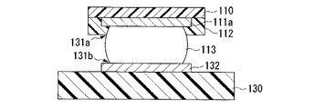
図17は従来のCSP等の電子部品(以下、半導体装置とも呼ぶ)の構造を例示する断面図であり、半導体装置において半田バンプを設ける部分を拡大して示すものである。
図17において、110は第一絶縁部であり、不図示の回路を一方の面上に設けたウエハからなる半導体基板(以下、半導体チップとも呼ぶ)の表層部に配置されている。111は第一導電部であり、この回路に導通し、半導体基板の第一絶縁部110の表面に形成されている。112は第二絶縁部であり、第一導電部111の外周部と第一絶縁部110を覆うように形成されている。113は半田バンプであり、露出された第一導電部111を覆うように設けられている。従来の半導体装置において半田バンプを設ける部分は、上述した第一絶縁部110、第一導電部111、第二絶縁部112、半田バンプ113から構成されている。
FIG. 17 is a cross-sectional view illustrating the structure of a conventional electronic component such as a CSP (hereinafter also referred to as a semiconductor device), and shows an enlarged portion where a solder bump is provided in the semiconductor device.
In FIG. 17,
図17に示すような半球状の半田バンプ113は、第一導電部111上に半田材料を形成した後、加熱処理(以下、リフロー処理とも呼ぶ)を施すことにより得られる。
第一導電部111上にまず半田を設ける方法としては、例えば(イ)電解半田めっき法、(ロ)半田ボール搭載法、(ハ)半田ペースト印刷法、(ニ)半田ペーストディスペンス法、(ホ)半田蒸着法などの製法が一般に使用されている。いずれの製法も、ウエハ全面の電極配置位置に、半田バンプ下部が所定の形状となるように形成された、半田と濡れ性の良い表面性状とした第一導電部111上に、所定の面積および高さを持つ半田材料を形成するものである。
A
For example, (a) electrolytic solder plating method, (b) solder ball mounting method, (c) solder paste printing method, (d) solder paste dispensing method, (ho) ) Manufacturing methods such as solder vapor deposition are generally used. In any of the manufacturing methods, on the first
各製法ごとに異なる半田材料が使用される。製法(イ)では半田成分を含有するめっき層が、製法(ロ)では予め所定のバンプ径に近い形状に分粒された半田ボールが、それぞれ用いられる。製法(ハ)や製法(ニ)では所定のバンプ径に比較して微細な半田粒子をフラックス成分に混合した印刷用のペースト状の半田を用いる。製法(ホ)では真空中で蒸着法により形成された半田成分を含有する金属蒸着膜を使用する。 Different solder materials are used for each manufacturing method. In the manufacturing method (a), a plating layer containing a solder component is used, and in the manufacturing method (b), solder balls that are sized in advance to a shape close to a predetermined bump diameter are used. In the manufacturing method (c) or manufacturing method (d), a paste solder for printing in which fine solder particles are mixed with a flux component in comparison with a predetermined bump diameter is used. In the manufacturing method (e), a metal vapor deposition film containing a solder component formed by a vapor deposition method in a vacuum is used.
いずれの製法により形成された半田であっても、リフロー処理時に半田を融点以上の温度に到達させることによって、半田は溶融し、溶融した半田は表面張力により凝集する。その形状は、下地をなす第一導電部111の周縁における金属の濡れ性、溶融した半田の表面張力、溶融した半田自体の重さによる変形、第一導電部111の外周部を覆う第二絶縁部112の端部形状など等により決定される。溶融した半田は、リフロー処理の後半において、半田の融点より低い温度で冷却処理を施すことにより固体となる。その結果、いわゆる半田バンプと呼ばれる球状に近い形状の半田塊が得られる。
Regardless of the solder formed by any of the manufacturing methods, when the solder reaches a temperature equal to or higher than the melting point during the reflow process, the solder is melted and the melted solder is agglomerated by the surface tension. The shape is the metal wettability at the periphery of the first
このような半田バンプを有する半導体装置では、その性能向上のために種々の改良が提案されている(例えば、特許文献1参照)。 In the semiconductor device having such a solder bump, various improvements have been proposed to improve its performance (see, for example, Patent Document 1).
図18は、従来の電子部品の実装時、半田バンプにくびれが生じた状態を示す断面図であり、図17に示した半導体装置を例とした場合である。ここで、半導体装置から半田バンプ113を除いた部分を半導体パッケージと呼ぶことにする。
FIG. 18 is a cross-sectional view showing a state in which a solder bump is constricted when a conventional electronic component is mounted, and is a case where the semiconductor device shown in FIG. 17 is taken as an example. Here, the part excluding the
図18は、半田バンプ113を回路基板(第二基板とも呼ぶ)の表層部に配置されている第二絶縁部130上の第二導通部132(電極パッドとも呼ぶ)に押し付けることにより、半導体装置(以下では、半導体チップとも呼ぶ)が回路基板に実装される様子を示している。なお、図17及び図18には半田バンプ113を突出させた状態で導電層を覆うように第二絶縁部(封止層とも呼ぶ)112を設けた例を示しているが、封止層は必須要件ではない。
FIG. 18 shows a semiconductor device in which a
つまり、上述した半田バンプ113は、半導体基板の第一導電部111と回路基板の第二導電部132との電気的な導通を図るための電極端子として機能するとともに、両者の熱変形や反りによって発生する応力を緩和、吸収する役割も担う。
That is, the above-described
しかしながら、図17に示すように、従来の半田バンプはその側面方向から見て半球状に近い。また、従来の半田バンプ113は第一導電部111に載置された状態では、半田バンプ113が第一導電部111と接してなる面は円形をなす傾向がある。特に、回路基板に実装した半導体パッケージでは、主に半導体チップと回路基板との熱膨張率の違いにより発生する応力を、回路基板から半導体チップが受ける。
However, as shown in FIG. 17, the conventional solder bump is nearly hemispherical when viewed from the side. In addition, when the
このため、半田バンプ113は、第一導電部111や第二導電部132と接触する接合部に応力の集中が発生しやすい。より具体的には、半田バンプ113はその外周面が、束縛された状態から解放された状態に変わる領域(くびれ部とも呼ぶ)131a、131bに応力が加わると、図17に示すように、例えば半田バンプ113の中にクラック(亀裂とも呼ぶ)115が外側から内側の方向に発生する傾向にあった。このようなクラック115の発生は断線不良を招き、ひいては半田バンプ113の破壊をもたらす恐れがあることから、半導体パッケージの信頼性を著しく低下させる原因の一つとして挙げられている。そこで、半田バンプの強度を上げることにより、半田バンプのくびれ部におけるクラックの発生を抑制するとともに、たとえクラックが発生したとしても断線不良には至ることのない構成を備えた電子部品及び電子装置の開発が期待されていた。
本発明は上記事情に鑑みてなされたもので、半田バンプの強度を向上させることにより、半田バンプのくびれ部におけるクラックの発生を抑制することが可能であり、かつ、半田バンプのくびれ部においてクラックが発生しても断線不良を起こさず、半田バンプの破壊を防止できる電子部品及び電子装置の提供を目的とする。 The present invention has been made in view of the above circumstances, and by improving the strength of the solder bumps, it is possible to suppress the occurrence of cracks in the constricted portions of the solder bumps, and cracks in the constricted portions of the solder bumps. An object of the present invention is to provide an electronic component and an electronic device that can prevent breakage of solder bumps without causing a disconnection failure even if the occurrence of the above occurs.
本発明に係る電子部品は、第一基板と第二基板が対向して配置され、前記第一基板の絶縁性を有する一面側に配された複数個の第一導電部と、前記第二基板の電気絶縁性を有する一面側に配された複数個の第二導電部との間に、個別に半田バンプを設けてなる電子部品であって、少なくとも1つの半田バンプにおいては、前記第一導電部において前記半田バンプと接する側の一面は、絶縁層で被覆された外周部と、前記第一導電部と接して配される凸部を備えた内周部とから構成されており、前記凸部は、前記半田バンプより大きな強度をもつ部材からなり、前記凸部の上面は、前記第一導電部から半田バンプの高さ方向において、半田バンプのくびれ部より突出した位置にあると共に、前記凸部の側面は第一導電部の一面と略垂直をなしており、前記半田バンプは少なくとも前記凸部の一部と前記内周部とを覆うように配設されていることを特徴としている。 An electronic component according to the present invention includes a first substrate and a second substrate facing each other, a plurality of first conductive portions disposed on one surface side having insulating properties of the first substrate, and the second substrate An electronic component in which solder bumps are individually provided between a plurality of second conductive portions disposed on one surface side having electrical insulation, wherein at least one solder bump has the first conductive One surface of the portion in contact with the solder bump is composed of an outer peripheral portion covered with an insulating layer and an inner peripheral portion provided with a convex portion arranged in contact with the first conductive portion. The portion is made of a member having a strength higher than that of the solder bump, and the upper surface of the convex portion is in a position protruding from the constricted portion of the solder bump in the height direction of the solder bump from the first conductive portion, and The side surface of the convex part is substantially perpendicular to one surface of the first conductive part. Ri, the solder bump is characterized by being arranged to cover at least the portion between the inner peripheral portion of the convex portion.
従来の半田バンプは、第一導電部の内周部と接して配される凸部を持たないか、あるいは凸部を有してもその凸部は台形状をなしていたため、第一基板や第二基板に外力が加わると、半田バンプがこれらの基板と接合されている部分あるいはその近傍に応力が集中し、クラック発生などが発生し、そのクラックは半田バンプの中を横断する方向に延びやすく、その結果、断線不良を生じたり、あるいは半田バンプの破壊を招いていた。 The conventional solder bump does not have a convex portion arranged in contact with the inner peripheral portion of the first conductive portion, or even if it has a convex portion, the convex portion has a trapezoidal shape. When an external force is applied to the second board, stress concentrates at or near the part where the solder bumps are bonded to these boards, and cracks occur. The cracks extend in a direction transverse to the solder bumps. As a result, disconnection failure occurred or solder bumps were destroyed.
これに対し、本発明に係る電子部品を構成する少なくとも1つの半田バンプは、その内部に凸部を備え、かつ、その凸部は、前記半田バンプより大きな強度をもつ部材から構成されており、半田バンプにより包み込まれた状態にある。このように内包された半田バンプより大きな強度をもつ部材からなる凸部は、半田バンプにおいてコア(核とも呼ぶ)として機能する。つまり、このようにコアを設けた半田バンプはそれ自体より強度の大きな芯を備えることになるので、半田バンプに外力が加わった際、半田バンプの外力に対抗する能力の向上が図れる。ゆえに、半田バンプのくびれ部におけるクラックの発生を抑制することが可能な電子部品が得られる。なお、上記大きな強度とは、凸部をなす部材が、実仕様温度域(−40℃〜125℃)において半田よりも降伏応力が大きく、かつ、ヤング率が大きいことを意味する。 On the other hand, at least one solder bump constituting the electronic component according to the present invention has a convex portion therein, and the convex portion is composed of a member having a strength higher than that of the solder bump, It is in a state of being encased by solder bumps. The convex portion made of a member having a strength higher than that of the encapsulated solder bump functions as a core (also referred to as a nucleus) in the solder bump. That is, since the solder bump provided with the core as described above has a core having a higher strength than the core itself, when the external force is applied to the solder bump, the ability to counter the external force of the solder bump can be improved. Therefore, an electronic component capable of suppressing the occurrence of cracks at the constricted portion of the solder bump is obtained. In addition, the said big intensity | strength means that the member which makes a convex part has a yield stress larger than a solder in a real specification temperature range (-40 degreeC-125 degreeC), and its Young's modulus is large.
また、半田バンプより大きな強度をもつ部材からなるコアの場合、コアのサイズを変更することにより、そのコアを内包してなる半田バンプの外力に対する強度を向上させつつ、強度の大きさを制御することも可能となる。強度の大きさを制御する手法としては、例えばコアの面積や高さを調整する方法が好適に用いられる。 Also, in the case of a core made of a member having a strength higher than that of the solder bump, by changing the size of the core, the strength against the external force of the solder bump including the core is improved and the magnitude of the strength is controlled. It is also possible. As a method for controlling the magnitude of the strength, for example, a method of adjusting the area and height of the core is preferably used.
さらに、前記凸部の上面は、前記第一導電部から半田バンプの高さ方向において、半田バンプのくびれ部より突出した位置にあると共に、前記凸部の側面は第一導電部の一面と略垂直をなしていることから、基板との接合部から半田バンプの中を横断する方向にクラックが延びてきた場合、そのクラックの先頭部は凸部の側面にほぼ垂直に衝突するので、凸部を越えてクラックが延びるのを確実に防止できる。ゆえに、本発明によれば、実装後に半田バンプのくびれ部においてクラックが発生しても断線不良を起こさず、半田バンプの破壊を防止できる電子部品が得られる。なお、上記略垂直とは、凸部の側面と第一導電部の一面とがなす角度が45度〜135度の範囲内にあることを指す。45度より狭い角度ではクラック進展を阻止する能力に乏しい。135度を超えるものは作製が極めて困難である。よって、45度以上135度以下のとき、上述したクラック進展阻止の作用が得られる。 Furthermore, the upper surface of the convex portion is located at a position protruding from the constricted portion of the solder bump in the height direction of the solder bump from the first conductive portion, and the side surface of the convex portion is substantially the same as one surface of the first conductive portion. Since cracks extend in the direction transverse to the inside of the solder bumps from the joints with the board because they are vertical, the tops of the cracks collide almost perpendicularly with the side surfaces of the protrusions. It is possible to reliably prevent the cracks from extending beyond. Therefore, according to the present invention, it is possible to obtain an electronic component capable of preventing breakage of the solder bump without causing disconnection failure even if a crack occurs in the constricted portion of the solder bump after mounting. The term “substantially perpendicular” means that the angle formed between the side surface of the convex portion and one surface of the first conductive portion is within a range of 45 degrees to 135 degrees. At an angle narrower than 45 degrees, the ability to prevent crack growth is poor. Those exceeding 135 degrees are extremely difficult to produce. Therefore, when the angle is not less than 45 degrees and not more than 135 degrees, the above-described action of preventing crack growth is obtained.
さらにまた、本発明に係る半田バンプはその内部に少なくとも前記凸部の一部を備えているので、上述した半田バンプが凸部を内包する構成とした際に得られる作用が働く。
したがって、かかる構成の半田バンプを備えてなる電子部品は、基板間の安定した導通を長期に亘って維持できる
Furthermore, since the solder bump according to the present invention has at least a part of the convex portion therein, the action obtained when the above-described solder bump includes the convex portion is effective.
Therefore, the electronic component including the solder bump having such a configuration can maintain stable conduction between the substrates over a long period of time.
かかる構成からなる電子部品において、凸部は、導電性部材、絶縁性部材の何れであってもよい。導電性部材を用いた場合は、半田バンプ内に導通の障害となる部分が存在しないので、従来と同様の導通特性が確保されるので好ましい。絶縁部材を用いた場合は、例えば半田バンプと弾性特性が大きく異なる部材が採用できるので、半田バンプのくびれ部におけるクラックが発生が抑制され、クラックが発生し半田バンプ内に延びてきても、そのクラックの先端部を弾力的な凸部が緩衝体となり確実に受け止めることができるので望ましい。 In the electronic component having such a configuration, the convex portion may be either a conductive member or an insulating member. The use of a conductive member is preferable because there is no portion that hinders conduction in the solder bump, and the same conduction characteristics as in the conventional case are ensured. In the case of using an insulating member, for example, a member having a greatly different elastic property from that of a solder bump can be adopted, so that the occurrence of a crack in the constricted portion of the solder bump is suppressed, and even if the crack occurs and extends into the solder bump, It is desirable because the elastic convex portion can be a buffer body and can reliably receive the tip of the crack.
本発明に係る電子部品において、凸部は、第一導電部の一面に接して配される形態A、
第一基板と第一導電部との間に設けられ、第一基板の一面と接して配される形態B、あるいは第一導電部を貫通するとともに、前記第一基板の一面と接して配される形態C、の何れであっても構わない。
In the electronic component according to the present invention, the convex portion is arranged in contact with one surface of the first conductive portion A,
Form B provided between the first substrate and the first conductive portion and arranged in contact with one surface of the first substrate, or penetrating the first conductive portion and disposed in contact with the one surface of the first substrate. Either form C may be used.
形態Aとした場合は、凸部が導電性部材と絶縁性部材の何れであっても、凸部と半田バンプは両方とも必ず第一導電部の一面に接して設けられる。この構成によれば、凸部の高さを精密に制御できることから、設計および製造が容易になるので好ましい。特に、凸部として金属からなる導電性部材を採用した場合は、凸部と第一導電部との界面を金属−金属接合とすることが可能なので、コアと下地との密着力を向上も図れるという長所を併せ持つことができる。凸部として絶縁性部材を採用した場合は、コアが強度に加えて異質の柔軟性も併せ持つことができる。 In the case of Form A, regardless of whether the convex portion is a conductive member or an insulating member, both the convex portion and the solder bump are always provided in contact with one surface of the first conductive portion. According to this configuration, since the height of the convex portion can be precisely controlled, it is preferable because design and manufacture are facilitated. In particular, when a conductive member made of metal is used as the convex portion, the interface between the convex portion and the first conductive portion can be made a metal-metal bond, so that the adhesion between the core and the base can be improved. You can also have the advantage of. When an insulating member is employed as the convex portion, the core can have a different kind of flexibility in addition to the strength.
形態Bとした場合は、凸部が第一基板と第一導電部との間に設けられ、第一基板の一面と接して配される。この構成によれば、半田との密着性を考慮しなくても良いので、凸部をなす部材の選択の幅が広くなる。凸部が導電性部材でなくても、良好な電気特性が確保される。特に、凸部が絶縁性部材の場合は、その上に第一導電部が配され、半田バンプとの電気的接合に寄与する面積が広がることになるので、第一導電部を設けなかった場合に比べて電気抵抗を小さくできる。 In the case of Form B, the convex portion is provided between the first substrate and the first conductive portion, and is arranged in contact with one surface of the first substrate. According to this configuration, it is not necessary to consider the adhesiveness to the solder, so that the range of selection of the member forming the convex portion is widened. Even if the convex portion is not a conductive member, good electrical characteristics are ensured. In particular, when the convex part is an insulating member, the first conductive part is arranged on the convex part, and the area contributing to the electrical bonding with the solder bumps is expanded. The electrical resistance can be reduced compared to.
形態Cとした場合は、凸部が第一導電部を貫通するとともに、電気絶縁性を有する第一基板の一面と接して設けられる。この構成によれば、凸部が導電性部材と絶縁性部材の何れであっても、凸部のうち一部(第一基板の一面と接する部分)が第一導電部内部に埋設されているので、凸部はその足下が強固に保持された状態となる。ゆえに、このような凸部を内包する半田バンプは、外力に対する抗力の向上が図れる。凸部が絶縁性部材の場合は、凸部と第一基板との界面を絶縁体−絶縁体接合とすることが可能なので、コアと下地との密着力を向上できる。凸部として絶縁性部材を採用した場合は、コアが強度に加えて異質の柔軟性も併せ持つことができるので好ましい。凸部が導電性部材の場合、凸部自体が第一導電部としても働くことから、良好な電気抵抗が維持される。 In the case of Form C, the convex portion penetrates the first conductive portion and is provided in contact with one surface of the first substrate having electrical insulation. According to this structure, even if a convex part is any of an electroconductive member and an insulating member, a part (part which contact | connects one surface of a 1st board | substrate) among convex parts is embed | buried in the inside of a 1st conductive part. Therefore, the convex portion is in a state where its feet are firmly held. Therefore, the solder bump including such a convex portion can improve the resistance against an external force. When the convex portion is an insulating member, the interface between the convex portion and the first substrate can be an insulator-insulator bond, so that the adhesion between the core and the base can be improved. When an insulating member is adopted as the convex portion, it is preferable because the core can have a different flexibility in addition to the strength. In the case where the convex portion is a conductive member, the convex portion itself also functions as the first conductive portion, so that good electrical resistance is maintained.
また、本発明に係る電子部品において、半田バンプは、前記凸部を全て被覆する形態Dであってもよいし、前記凸部の中央部のみを被覆する形態Eであっても構わない。
形態Dとした場合は、半田バンプ内に凸部は内包されるので、半田バンプを複数配する際に、半田バンプ同士の間隔に凸部は影響を与えることなく、半田バンプの外力に対する抗力を改善できる。
形態Eとした場合は、半田バンプのサイズに制限されることなく、大型の凸部(面積や高さ、体積という観点から)を配することができる。大型の凸部は作製が容易であり、かつ、外力を受けやすい方向に大きな側面をなど特殊な形状を採ることも可能である。
Moreover, in the electronic component according to the present invention, the solder bump may be in a form D that covers all the convex portions or in a form E that covers only the central portion of the convex portions.
In the case of Form D, since the convex part is included in the solder bump, when arranging a plurality of solder bumps, the convex part does not affect the distance between the solder bumps, and the resistance against the external force of the solder bump is exerted. Can improve.
In the case of Form E, a large convex portion (in terms of area, height, and volume) can be disposed without being limited by the size of the solder bump. Large protrusions can be easily manufactured, and can take a special shape such as a large side surface in a direction in which external forces are easily received.
さらに、本発明に係る電子部品において、前記第一導電部は、凸部ごとに第一導電部を一つ配した形態Fであってもよいし、凸部ごとに第一導電部を複数個配した形態Gであっても構わない。
形態Fとした場合は、凸部を設ける第一導電部が、第一基板のどの様な場所に位置するのかを考慮して、半田バンプが好ましい強度を有するように、凸部を構成する部材を選択配置できる。
形態Gとした場合は、凸部が接する第一導電部を複数に分断することで、半田バンプ内を進行するクラック(亀裂)は、この分断された箇所においてその進行が阻まれる。ゆえに、第一導電部を複数に分断してなる構成は、クラック(亀裂)の進展を止めることができる。
Furthermore, in the electronic component according to the present invention, the first conductive portion may be in a form F in which one first conductive portion is arranged for each convex portion, or a plurality of first conductive portions are provided for each convex portion. The arranged form G may be used.
In the case of Form F, in consideration of where the first conductive portion for providing the convex portion is located on the first substrate, the member constituting the convex portion so that the solder bump has a preferable strength Can be selected and placed.
In the case of Form G, by dividing the first conductive portion in contact with the convex portion into a plurality, cracks that progress in the solder bumps are prevented from progressing at the divided locations. Therefore, the structure which divides | segments the 1st electroconductive part into plurality can stop progress of a crack (crack).
本発明に係る電子装置は、上述した構成の電子部品を含むことを特徴としている。上述した構成の電子部品は、実装後に断線不良や半田バンプの破壊を防止する構造を具備したことにより、基板間の安定した導通を長期に亘って維持できるので、長期信頼性に優れた電子部品の提供が可能となる。 An electronic device according to the present invention includes the electronic component having the above-described configuration. The electronic component having the above-described structure has a structure that prevents disconnection failure and solder bump destruction after mounting, so that stable conduction between substrates can be maintained over a long period of time, so that the electronic component has excellent long-term reliability. Can be provided.
以上説明したように、本発明に係る電子部品を構成する半田バンプは少なくともその内部に凸部を備え、この凸部は半田バンプより大きな強度をもつ部材から構成され、この凸部の上面は半田バンプのくびれ部より突出した位置にあると共に、前記凸部の側面は第一導電部の一面と略垂直をなす構成を有する。したがって、外力や熱の影響を受けた場合に半田バンプの付け根に相当する導電部との接合付近(くびれ部)への応力集中が発生した際に、これに起因して、基板との接合部から半田バンプの中を横断する方向にクラックが発生するのを抑え
るとともに、たとえクラックが発生しても上記凸部がクラックの進行を阻止するように機能する。
As described above, the solder bump constituting the electronic component according to the present invention has at least a convex portion therein, and the convex portion is formed of a member having a strength higher than that of the solder bump, and the upper surface of the convex portion is soldered. The bumps are in a position protruding from the constricted portion of the bump, and the side surface of the convex portion is configured to be substantially perpendicular to one surface of the first conductive portion. Therefore, when stress concentration occurs near the joint (constriction) with the conductive part corresponding to the base of the solder bump when affected by external force or heat, the joint with the board is caused by this. Thus, the occurrence of cracks in the direction transverse to the solder bumps is suppressed, and even if a crack occurs, the protrusion functions to prevent the crack from proceeding.
ゆえに、本発明は、実装後に断線不良や半田バンプの破壊を防止できる電子部品をもたらす。換言すると、本発明は、実装後に半田バンプにクラックが発生した場合に生じていた電気的接続に関する不具合を防止できるので、長期信頼性の高い電子部品の提供に寄与するとともに、電気的接続の信頼性も向上させる。 Therefore, the present invention provides an electronic component that can prevent disconnection failure and solder bump destruction after mounting. In other words, the present invention can prevent a failure related to electrical connection that has occurred when a solder bump cracks after mounting, thereby contributing to the provision of electronic components with high long-term reliability and reliability of electrical connection. Improves performance.
以下では、本発明に係る電子部品の一実施形態を図面に基づいて説明する。図1〜図8は絶縁性の凸部を用いた場合を、図9〜図14は導電性の凸部を用いた場合を、それぞれ表している。
なお、以下では、第一基板の少なくとも1つの第一導電部に凸部がある場合について詳細に説明するが、これに代えて、第二基板の少なくとも1つの第二導電部に凸部を設けた形態としても同様の作用・効果が得られることは言うまでもない。
Below, one Embodiment of the electronic component which concerns on this invention is described based on drawing. 1 to 8 show cases where insulating convex portions are used, and FIGS. 9 to 14 show cases where conductive convex portions are used.
In the following, the case where the at least one first conductive portion of the first substrate has a convex portion will be described in detail, but instead, at least one second conductive portion of the second substrate is provided with a convex portion. It goes without saying that the same action and effect can be obtained even in the case of a different form.
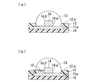
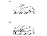
図1は、本発明に係る電子部品の作製に用いる第一基板の一例を示す部分断面図であり、一つの第一導電部11a上に導電性の凸部14が配され、これらを覆うように半田13を設けた場合である。この半田13は、第一基板を第二基板に実装した際に、第一基板と第二基板で挟まれることによりバンプとして機能することから、以下では半田バンプとも呼ぶ。
FIG. 1 is a partial cross-sectional view showing an example of a first substrate used for manufacturing an electronic component according to the present invention. A conductive
図1において、(a)は半田バンプに外力が印加されていない状態を、(b)は半田バンプに外力が印加され、半田バンプにクラックが発生した状態を、それぞれ表している。その際、導電性の凸部14としては、半田バンプより大きな強度をもつ部材が用いられる。例えば、スズや鉛、銀、銅等の材料からなる半田バンプに対しては、導電性の凸部14をなす部材としては、銅やニッケル、亜鉛、スズ、鉛、クロム、銀、金等が好適に用いられる。
1A shows a state where no external force is applied to the solder bump, and FIG. 1B shows a state where an external force is applied to the solder bump and a crack is generated in the solder bump. At this time, a member having a strength higher than that of the solder bump is used as the conductive
図1において、10は第一絶縁部であり、不図示の回路を一方の面上に設けたウエハからなる半導体基板(以下、半導体チップとも呼ぶ)の表層部に配置されている。11aは第一導電部であり、この回路に導通し、半導体基板の第一絶縁部10の表面に形成されている。12は第二絶縁部であり、第一導電部11の外周部と第一絶縁部10を覆うように形成されている。13は半田バンプであり、露出された第一導電部11を覆うように設けられている。
In FIG. 1,
半田バンプ13の内部には、凸部14が次に述べるような位置に配されている。
すなわち、第一導電部11において半田バンプ13と接する側の一面は、第二絶縁部12からなる第二絶縁部12をなす絶縁層で被覆された外周部と、第一導電部11と接して配される凸部14を備えた内周部とから構成されている。そして、この凸部14は、第一導電部11aの一面と略垂直をなす側面14αと前記絶縁層(第二絶縁部)の表面12αより突出した位置にある上面14βとを有しており、半田バンプ13は少なくとも凸部14の一部と前記内周部とを覆うように配設されている。
Inside the solder bumps 13,
That is, one surface of the first conductive portion 11 that is in contact with the
かかる構成によれば、半田バンプ13の内部に設けられた凸部14は、第一導電部11の一面と略垂直をなす側面14aと前記絶縁層の表面12αより突出した位置にある上面14βとを有しているので、たとえば図1(b)に示すように、基板との接合部から半田バンプの中を横断する方向にクラック15が延びてきた場合であっても、そのクラック15の先頭部は凸部14の側面14αにほぼ垂直に衝突するので、凸部14を越えてクラック15が延びるのを確実に防止できる。その結果、実装後に断線不良や半田バンプの破壊を確実に防止することが可能となる。特に、図1に示した例においては、凸部14が導電性の部材から構成されているので、凸部14の存在自体が上下基板間における電気的導通を阻害する要因とはなりにくい。
According to such a configuration, the
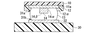
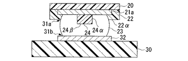
図2は本発明に係る電子部品の部分断面図であり、第一基板を第二基板に実装した状態を示している。図2において、30は第三絶縁部であり、第二基板(以下、回路基板とも呼ぶ)の表層部に配置されている。32は第二導電部であり、第三絶縁部30の表面に形成されており、半田バンプ13を介して第一基板の第一導電部11aと電気的な接続を図るために用いられる。
FIG. 2 is a partial cross-sectional view of the electronic component according to the present invention, and shows a state where the first substrate is mounted on the second substrate. In FIG. 2,
図2に示すように、第一基板を第二基板に実装すると、対向する一組の導電部11a、32間に半田バンプ13が挟まれた状態となる。その結果、半田バンプ13の各導電部11a、32と接合部(いわゆる、付け根)の外周にはくびれ部31a、31bが形成される。前述したクラック15は、このくびれ部31a、31bから半田バンプ13の内部に進行するように発生する傾向にある。
ところが、本発明に係る電子部品では、導電性の部材からなる凸部14が半田バンプ13の中に設けてあるので、半田バンプ13の外力に対する強度的な改善が図れることから、クラック15の発生を抑制できる。また、本発明に係る電子部品では、上記形態の凸部14を半田バンプ13内に予め設けてあるので、くびれ部31a、31bから半田バンプ内へクラック15が進行しても、凸部14がその進行を阻害する構造物として機能するので、クラック15が凸部14を越えてさらに進行し、半田バンプ13の破壊をもたらす恐れはない。
As shown in FIG. 2, when the first substrate is mounted on the second substrate, the solder bumps 13 are sandwiched between the pair of
However, in the electronic component according to the present invention, since the
図3は、本発明に係る電子部品の作製に用いる第一基板の他の一例を示す部分断面図であり、半導体基板の第一絶縁部10と一つの第一導電部11bとの間に導電性の凸部14が配され、第一導電部11bを覆うように半田バンプ13を設けた場合である。
この構成によれば、凸部には強度を確保する働きをもたせると共に、第一導電部には電気抵抗を小さくする働きをもたせるように、機能分離させた構造を採用できる。その際、導電性の凸部14としては、半田バンプより大きな強度をもつ部材が用いられる。例えば、スズ、銀、銅、リン、ニッケル等の材料からなる半田バンプに対しては、導電性の凸部14をなす部材としては、導電性セラミックス、導電性樹脂等が、第一導電部11bをなす部材としては、銅、金、ニッケル、アルミニウム等が好適に用いられる。
FIG. 3 is a partial cross-sectional view showing another example of the first substrate used for the production of the electronic component according to the present invention. The first
According to this configuration, it is possible to employ a function-separated structure so that the convex portion has a function of ensuring strength and the first conductive portion has a function of reducing electrical resistance. At this time, a member having a strength higher than that of the solder bump is used as the conductive
図4は、本発明に係る電子部品の作製に用いる第一基板の他の一例を示す部分断面図であり、一つの第一導電部11cを貫通して半導体基板の第一絶縁部10上に導電性の凸部14が配され、第一導電部11cと凸部14とを覆うように半田13を設けた場合である。
この構成によれば、凸部14のうち一部(第一基板10の一面と接する部分)が第一導電部11c内部に埋設されているので、凸部14はその足下が強固に保持された状態となる。ゆえに、このような凸部14を内包する半田バンプ13は、外力に対する抗力の向上が図れる。また、凸部14が導電性部材からなるので、第一導電部11cのうち凸部14を埋設するため欠落した部分も導電性を有することが可能なので、良好な電気抵抗が維持される。その際、導電性の凸部14としては、半田バンプより大きな強度をもつ部材が用いられる。例えば、スズ、亜鉛、ビスマス等の材料からなる半田バンプに対しては、導電性の凸部14をなす部材としては、銅、金、ニッケル、モリブデン等が、第一導電部11cをなす部材としては、ニッケル、アルミニクム、銅、金等が好適に用いられる。
FIG. 4 is a partial cross-sectional view showing another example of the first substrate used for manufacturing the electronic component according to the present invention, penetrating through one first
According to this configuration, a portion of the convex portion 14 (a portion in contact with one surface of the first substrate 10) is embedded in the first
図5は、本発明に係る電子部品の作製に用いる第一基板を構成する半田を上方から見た平面図であり、半田13の中に正方形をなす導電性の凸部14aが全て内包されるように設けた場合である。
この構成によれば、半田バンプ13内に凸部14aは内包されるので、第一基板(不図示)の上に半田バンプ13を複数配置したり、サイズの小さな半田バンプ13に対応させる場合などにおいて、半田バンプ同士の間隔に凸部は影響を与えることなく、半田バンプの外力に対する抗力を改善できる。また、凸部14aが、第一基板(不図示)のどの様な場所に位置するのかを考慮して、半田バンプ13が好ましい強度を有するように、凸部14aを構成する部材を選択配置できる。図5には凸部14aが上方(半田バンプ側)から見て正方形をなす例を示したが、その形状は限定されるものではない。例えば、円形や楕円形等でもよいし、長方形や多角形等など各種の矩形であっても構わない。その際、導電性の凸部14aとしては、半田バンプより大きな強度をもつ部材が用いられる。例えば、スズ、インジウム、アンチモン等の材料からなる半田バンプに対しては、導電性の凸部14aをなす部材としては、チタン、タングステン、シリコン、ゲルマニウム等が好適に用いられる。
FIG. 5 is a plan view of the solder constituting the first substrate used for manufacturing the electronic component according to the present invention as viewed from above. The
According to this configuration, since the
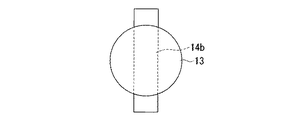
図6は、本発明に係る電子部品の作製に用いる第一基板を構成する半田を上方から見た平面図であり、半田13の中を貫通し、その両端部が半田13の外部に突き出るように、長方形をなす導電性の凸部14bを設けた場合である。
この構成によれば、半田バンプ13のサイズに制限されることなく、大型の凸部14b(面積や高さ、体積という観点から)を配することができる。大型の凸部14bは作製が容易であり、かつ、外力を受けやすい方向に大きな側面をなど特殊な形状を採ることも可能である。また、大型の凸部14bを設ける半田バンプ13が、第一基板(不図示)のどの様な場所に位置するのかを考慮して、半田バンプ13が好ましい強度を有するように、凸部14bを構成する部材を選択配置することもできる。その際、導電性の凸部14bとしては、半田バンプより大きな強度をもつ部材が用いられる。例えば、スズ、鉛、アルミニウム等の材料からなる半田バンプに対しては、導電性の凸部14bをなす部材としては、スズ、アモルファス炭素、金等が好適に用いられる。
FIG. 6 is a plan view of the solder constituting the first substrate used for manufacturing the electronic component according to the present invention as viewed from above, and penetrates through the
According to this configuration, the large
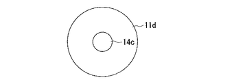
図7は、本発明に係る電子部品の作製に用いる第一基板を構成する第一導電部11dと導電性の凸部14cとを上方から見た平面図であり、凸部あたり一つの第一導電部11dを設けた場合である。
この構成によれば、凸部14cを設ける第一導電部11dが、第一基板(不図示)のどの様な場所に位置するのかを考慮して、半田バンプ(不図示)が好ましい強度を有するように、凸部14cを構成する部材を選択配置できる。図7には凸部14cが上方(半田バンプ側)から見て円形をなす例を示したが、その形状は限定されるものではない。例えば、円形の他に楕円形等でもよいし、正方形や長方形、多角形等など各種の矩形であっても構わない。その際、導電性の凸部14cとしては、半田バンプより大きな強度をもつ部材が用いられる。例えば、スズ、銀、ニッケル、コバルト等の材料からなる半田バンプに対しては、導電性の凸部14cをなす部材としては、アルミニウム、銀、モリブデン等が、第一導電部11dとしては、銅、クロム、チタン、タングステン等が好適に用いられる。
FIG. 7 is a plan view of the first
According to this configuration, the solder bump (not shown) has a preferable strength in consideration of where the first
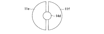
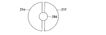
図8は、本発明に係る電子部品の作製に用いる第一基板を構成する第一導電部11e、11fと導電性の凸部14dとを上方から見た平面図であり、凸部あたり複数個の第一導電部11e、11fを設けた場合(図8は第一導電部が二つの場合を表す)である。
これは、凸部が接する第一導電部を複数に分断する構成であり、図8は2つに分断された第一導電部11e、11fを示した例である。この構成によれば、半田バンプ(不図示)内を進行するクラック(亀裂)は、この分断された箇所においてその進行が阻まれる。ゆえに、第一導電部を複数に分断してなる構成は、クラック(亀裂)の進展を止めることができる。図8には第一導電部を2つに分断した例を示したが、3つ以上に分断しても上述した作用は得られるので、第一導電部を分断する数は2つに限定されるものではない。その際、導電性の凸部14dとしては、半田バンプより大きな強度をもつ部材が用いられる。例えば、スズ、鉛、アンチモン等の材料からなる半田バンプに対しては、導電性の凸部14dをなす部材としては、チタン、タングステン、シリコン、ゲルマニウム等が、分断されてなる第一導電部11e、11fとしては、アルミニウム、シリコン−アルミニウム、ニッケル等が好適に用いられる。
FIG. 8 is a plan view of the first
This is a configuration in which the first conductive portion in contact with the convex portion is divided into a plurality of parts, and FIG. 8 is an example showing the first
図9は、本発明に係る電子部品の作製に用いる第一基板の他の一例を示す部分断面図であり、一つの第一導電部21a上に絶縁性の凸部24が配され、これらを覆うように半田23を設けた場合である。(a)は半田バンプに外力が印加されていない状態を、(b)は半田バンプに外力が印加され、半田バンプにクラックが発生した状態を、それぞれ表している。その際、絶縁性の凸部24としては、半田バンプより大きな強度をもつセラミック部材が用いられる。例えば、スズ、銅、鉛、アルミニウム等の材料からなる半田バンプに対しては、絶縁性の凸部24をなすセラミック部材としては、アルミナ、ジルコニア、シリカ、ジルコン、チタン酸アルミニウム、スピネル、窒化珪素、ダイヤモンド等が好適に用いられる。
FIG. 9 is a partial cross-sectional view showing another example of the first substrate used for manufacturing the electronic component according to the present invention. Insulating
図9において、20は第一絶縁部であり、不図示の回路を一方の面上に設けたウエハからなる半導体基板(以下、半導体チップとも呼ぶ)の表層部に配置されている。21aは第一導電部であり、この回路に導通し、半導体基板の第一絶縁部20の表面に形成されている。22は第二絶縁部であり、第一導電部21aの外周部と第一絶縁部20を覆うように形成されている。23は半田バンプであり、露出された第一導電部21を覆うように設けられている。
In FIG. 9,
半田バンプ23の内部には、凸部24が次に述べるような位置に配されている。
すなわち、第一導電部21aにおいて半田バンプ23と接する側の一面は、第二絶縁部22からなる第二絶縁部22をなす絶縁層で被覆された外周部と、第一導電部21aと接して配される凸部24を備えた内周部とから構成されている。そして、この凸部24は、第一導電部11aの一面と略垂直をなす側面24αと前記絶縁層(第二絶縁部)の表面22αより突出した位置にある上面24βとを有しており、半田バンプ23は少なくとも凸部24の一部と前記内周部とを覆うように配設されている。
Inside the solder bumps 23,
That is, one surface of the first
かかる構成によれば、半田バンプ23の内部に設けられた凸部24は、第一導電部21aの一面と略垂直をなす側面24αと前記絶縁層の表面22αより突出した位置にある上面24βとを有しているので、図9(b)に示すように、基板との接合部から半田バンプの中を横断する方向にクラック25が延びてきた場合、そのクラック25の先頭部は凸部24の側面24αにほぼ垂直に衝突するので、凸部24を越えてクラック25が延びるのを確実に防止できる。その結果、実装後に断線不良や半田バンプの破壊を確実に防止することが可能となる。特に、図9に示した例においては、凸部24が絶縁性の部材から構成されているので、導電性の半田バンプ23は、それ自体とは大きく物性の異なるセラミックからなる凸部24を内包した構成なので、半田バンプ23が外力を受けた際に、半田バンプ23内における力の伝搬が緩和される。
According to such a configuration, the
図10は本発明に係る電子部品の部分断面図であり、第一基板を第二基板に実装した状態を示している。図10において、30は第三絶縁部であり、第二基板(以下、回路基板とも呼ぶ)の表層部に配置されている。32は第二導電部であり、第三絶縁部30の表面に形成されており、半田バンプ23を介して第一基板の第一導電部21aと電気的な接続を図るために用いられる。
FIG. 10 is a partial cross-sectional view of the electronic component according to the present invention, and shows a state where the first substrate is mounted on the second substrate. In FIG. 10, 30 is a 3rd insulation part, and is arrange | positioned at the surface layer part of the 2nd board | substrate (henceforth a circuit board).
図10に示すように、第一基板を第二基板に実装すると、対向する一組の導電部21a、32間に半田バンプ23が挟まれた状態となる。その結果、半田バンプ23の各導電部21a、32と接合部(いわゆる、付け根)の外周にはくびれ部31a、31bが形成される。前述したクラック25は、このくびれ部31a、31bから半田バンプ23の内部に進行するように発生する傾向にある。
ところが、本発明に係る電子部品では、絶縁性の部材からなる凸部24が半田バンプ23の中に設けてあるので、半田バンプ23の外力に対する強度的な改善が図れることから、クラック25の発生を抑制できる。また、本発明に係る電子部品では、上記形態の凸部24を半田バンプ23内に予め設けてあるので、くびれ部31a、31bから半田バンプ内へクラック25が進行しても、凸部24がその進行を阻害する構造物として機能するので、クラック25が凸部24を越えてさらに進行し、半田バンプ23の破壊をもたらす恐れはない。
As shown in FIG. 10, when the first substrate is mounted on the second substrate, the solder bumps 23 are sandwiched between the pair of
However, in the electronic component according to the present invention, since the
図11は、本発明に係る電子部品の作製に用いる第一基板の他の一例を示す部分断面図であり、半導体基板の第一絶縁部20と一つの第一導電部21bとの間に絶縁性の凸部24が配され、第一導電部21bを覆うように半田バンプ23を設けた場合である。
この構成によれば、凸部24には強度を確保する働きをもたせると共に、第一導電部21bには電気抵抗を小さくする働きをもたせるように、機能分離させた構造を採用できる。その際、導電性の凸部24としては、半田バンプ23より大きな強度をもつ部材が用いられる。例えば、スズ、ビスマス、銅、銀等の材料からなる半田バンプ23に対しては、絶縁性の凸部24をなす絶縁部材としては、マグネシア、ベリリア、酸化トリウムフェライト、チタン酸バリウム等からなるセラミックが、第一導電部11bをなす部材としては、ニッケル、アルミニウム、銅等が好適に用いられる。
FIG. 11 is a partial cross-sectional view showing another example of the first substrate used for the production of the electronic component according to the present invention, in which insulation is provided between the first insulating
According to this configuration, the function-separated structure can be employed so that the
図12は、本発明に係る電子部品の作製に用いる第一基板の他の一例を示す部分断面図であり、一つの第一導電部21cを貫通して半導体基板の第一絶縁部20上に絶縁性の凸部24が配され、第一導電部21cと凸部24とを覆うように半田23を設けた場合である。
この構成によれば、凸部24のうち一部(第一基板20の一面と接する部分)が第一導電部21c内部に埋設されているので、凸部24はその足下が強固に保持された状態となる。ゆえに、このような凸部24を内包する半田バンプ23は、外力に対する抗力の向上が図れる。その際、絶縁性の凸部24としては、半田バンプより大きな強度をもつ絶縁部材が用いられる。例えば、スズ、銀、ビスマス、インジウム等の材料からなる半田バンプに対しては、絶縁性の凸部24をなす絶縁部材としては、ソーダガラス、石英ガラス、ホウケイ酸ガラス等が、第一導電部11cをなす部材としては、ニッケル、金、銅等が好適に用いられる。
FIG. 12 is a partial cross-sectional view showing another example of the first substrate used for manufacturing the electronic component according to the present invention, penetrating one first
According to this configuration, a portion of the convex portion 24 (a portion in contact with one surface of the first substrate 20) is embedded in the first
図13は、本発明に係る電子部品の作製に用いる第一基板を構成する半田を上方から見た平面図であり、半田23の中に正方形をなす絶縁性の凸部24aが全て内包されるように設けた場合である。
この構成によれば、半田バンプ23内に凸部24aは内包されるので、第一基板(不図示)の上に半田バンプ23を複数配置したり、サイズの小さな半田バンプ23に対応させる場合などにおいて、半田バンプ同士の間隔に凸部は影響を与えることなく、半田バンプの外力に対する抗力を改善できる。また、凸部24aが、第一基板(不図示)のどの様な場所に位置するのかを考慮して、半田バンプ23が好ましい強度を有するように、凸部24aを構成する部材を選択配置できる。図13には凸部24aが上方(半田バンプ側)から見て正方形をなす例を示したが、その形状は限定されるものではない。例えば、円形や楕円形等でもよいし、長方形や多角形等など各種の矩形であっても構わない。その際、絶縁性の凸部24aとしては、半田バンプより大きな強度をもつ絶縁部材が用いられる。例えば、スズ、亜鉛、アルミニウム等の材料からなる半田バンプに対しては、絶縁性の凸部24aをなす絶縁部材としては、窒化珪素、窒化アルミニウム、窒化チタン等からなるセラミックが好適に用いられる。
FIG. 13 is a plan view of the solder constituting the first substrate used for manufacturing the electronic component according to the present invention as viewed from above, and the insulating
According to this configuration, since the
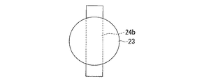
図14は、本発明に係る電子部品の作製に用いる第一基板を構成する半田を上方から見た平面図であり、半田23の中を貫通し、その両端部が半田23の外部に突き出るように、長方形をなす絶縁性の凸部24bを設けた場合である。
この構成によれば、半田バンプ23のサイズに制限されることなく、大型の凸部24b(面積や高さ、体積という観点から)を配することができる。大型の凸部24bは作製が容易であり、かつ、外力を受けやすい方向に大きな側面をなど特殊な形状を採ることも可能である。また、大型の凸部24bを設ける半田バンプ23が、第一基板(不図示)のどの様な場所に位置するのかを考慮して、半田バンプ23が好ましい強度を有するように、凸部24bを構成する部材を選択配置することもできる。その際、絶縁性の凸部24bとしては、半田バンプより大きな強度をもつ絶縁部材が用いられる。例えば、スズ、銀、銅ゲルマニウム等の材料からなる半田バンプに対しては、絶縁性の凸部24bをなす絶縁部材としては、炭化珪素、炭化硼素、炭化タングステン等からなるセラミックが好適に用いられる。
FIG. 14 is a plan view of the solder constituting the first substrate used for manufacturing the electronic component according to the present invention as viewed from above, and penetrates through the
According to this configuration, the large
図15は、本発明に係る電子部品の作製に用いる第一基板を構成する第一導電部21dと絶縁性の凸部24cとを上方から見た平面図であり、凸部あたり一つの第一導電部11dを設けた場合である。
この構成によれば、凸部24cを設ける第一導電部11dが、第一基板(不図示)のどの様な場所に位置するのかを考慮して、半田バンプ(不図示)が好ましい強度を有するように、凸部24cを構成する部材を選択配置できる。図15は凸部24cが上方(半田バンプ側)から見て円形をなす例を示したが、その形状は限定されるものではない。例えば、円形の他に楕円形等でもよいし、正方形や長方形、多角形等など各種の矩形であっても構わない。その際、絶縁性の凸部24cとしては、半田バンプより大きな強度をもつ部材が用いられる。例えば、スズ、亜鉛、アルミニウム、チタン等の材料からなる半田バンプに対しては、絶縁性の凸部24cをなす部材としては、ポリアミドイミドやポリエーテルエーテルケトン等の耐熱温度が半田の融点以上のプラスチック等が、第一導電部21dとしては、銅、チタン、タングステン、アルミニウム等が好適に用いられる。
FIG. 15 is a plan view of the first
According to this configuration, the solder bump (not shown) has a preferable strength in consideration of where the first
図16は、本発明に係る電子部品の作製に用いる第一基板を構成する第一導電部21e、21fと絶縁性の凸部24dとを上方から見た平面図であり、凸部あたり複数個の第一導電部21e、21fを設けた場合(図16は第一導電部が二つの場合を表す)である。
これは、凸部が接する第一導電部を複数に分断する構成であり、図16は2つに分断された第一導電部11e、11fを示した例である。この構成によれば、半田バンプ(不図示)内を進行するクラック(亀裂)は、この分断された箇所においてその進行が阻まれる。ゆえに、第一導電部を複数に分断してなる構成は、クラック(亀裂)の進展を止めることができる。図8には第一導電部を2つに分断した例を示したが、3つ以上に分断しても上述した作用は得られるので、第一導電部を分断する数は2つに限定されるものではない。その際、絶縁性の凸部24dとしては、半田バンプより大きな強度をもつ絶縁部材が用いられる。例えば、スズ、銀、亜鉛、銅、鉛等の材料からなる半田バンプに対しては、絶縁性の凸部24dをなす絶縁部材としては、ホウ化ジルコニウム、硫化カドミウム、酸化珪素等が、分断されてなる第一導電部11e、11fとしては、銀、アモルファス炭素、銅等が好適に用いられる。
FIG. 16 is a plan view of the first
This is a configuration in which the first conductive portion in contact with the convex portion is divided into a plurality of parts, and FIG. 16 is an example showing the first
本発明によれば、実装後における優れた耐久性と高い信頼性とを兼ね備えた電子部品及び電子装置を提供することができる。ゆえに、本発明は、外部からの衝撃などを受けやすい商品、例えば携帯電話やビデオカメラにおいて、耐衝撃性の改善や長期信頼性の向上をもたらす。 ADVANTAGE OF THE INVENTION According to this invention, the electronic component and electronic device which have the outstanding durability after mounting, and high reliability can be provided. Therefore, the present invention brings about improvement in impact resistance and long-term reliability in products that are susceptible to external impacts, such as mobile phones and video cameras.
10、20 第一絶縁部、11a〜11f、21a〜21f 第一導電部、12 22 第二絶縁部、13、23 半田(半田バンプ)、14 導電性の凸部、24 絶縁性の凸部、30 第三絶縁部、31a、31b くびれ部、32 第二導電部。
10, 20 1st insulation part, 11a-11f, 21a-21f 1st conductive part, 12 22 2nd insulation part, 13, 23 Solder (solder bump), 14 Conductive convex part, 24 Insulating convex part, 30 3rd insulation part, 31a, 31b Constriction part, 32 2nd electroconductive part.
Claims (11)
少なくとも1つの半田バンプにおいては、
前記第一導電部において前記半田バンプと接する側の一面は、絶縁層で被覆された外周部と、前記第一導電部と接して配される凸部を備えた内周部とから構成されており、
前記凸部は前記半田バンプより大きな強度をもつ部材からなり、
前記凸部の上面は、前記第一導電部から半田バンプの高さ方向において、半田バンプのくびれ部より突出した位置にあると共に、前記凸部の側面は第一導電部の一面と略垂直をなしており、
前記半田バンプは少なくとも前記凸部の一部と前記内周部とを覆うように配設されていることを特徴とする電子部品。 A first substrate and a second substrate are arranged to face each other, and a plurality of first conductive portions disposed on one surface side having insulation properties of the first substrate, and one surface side having electrical insulation properties of the second substrate. An electronic component in which solder bumps are individually provided between a plurality of second conductive portions arranged in
At least one solder bump
One surface of the first conductive portion on the side in contact with the solder bump is composed of an outer peripheral portion covered with an insulating layer and an inner peripheral portion provided with a convex portion arranged in contact with the first conductive portion. And
The convex portion is made of a member having a greater strength than the solder bump,
The upper surface of the convex portion is in a position protruding from the constricted portion of the solder bump in the height direction of the solder bump from the first conductive portion, and the side surface of the convex portion is substantially perpendicular to one surface of the first conductive portion. And
2. The electronic component according to claim 1, wherein the solder bump is disposed so as to cover at least a part of the convex portion and the inner peripheral portion.
An electronic device comprising the electronic component according to claim 1.
Priority Applications (1)
| Application Number | Priority Date | Filing Date | Title |
|---|---|---|---|
| JP2004106614A JP2005294482A (en) | 2004-03-31 | 2004-03-31 | Electronic component and electronic device |
Applications Claiming Priority (1)
| Application Number | Priority Date | Filing Date | Title |
|---|---|---|---|
| JP2004106614A JP2005294482A (en) | 2004-03-31 | 2004-03-31 | Electronic component and electronic device |
Publications (1)
| Publication Number | Publication Date |
|---|---|
| JP2005294482A true JP2005294482A (en) | 2005-10-20 |
Family
ID=35327084
Family Applications (1)
| Application Number | Title | Priority Date | Filing Date |
|---|---|---|---|
| JP2004106614A Pending JP2005294482A (en) | 2004-03-31 | 2004-03-31 | Electronic component and electronic device |
Country Status (1)
| Country | Link |
|---|---|
| JP (1) | JP2005294482A (en) |
Cited By (5)
| Publication number | Priority date | Publication date | Assignee | Title |
|---|---|---|---|---|
| WO2012127614A1 (en) * | 2011-03-22 | 2012-09-27 | ルネサスエレクトロニクス株式会社 | Semiconductor device |
| JP2014107427A (en) * | 2012-11-28 | 2014-06-09 | Shinko Electric Ind Co Ltd | Wiring board, semiconductor device and wiring board manufacturing method |
| WO2015098460A1 (en) * | 2013-12-27 | 2015-07-02 | 三菱マテリアル株式会社 | Solder bump having cored structure and production method therefor |
| JP2015126159A (en) * | 2013-12-27 | 2015-07-06 | 三菱マテリアル株式会社 | Core paste for forming sintered cores of solder bumps |
| US11631649B2 (en) | 2018-12-14 | 2023-04-18 | Olympus Corporation | Bonded body and manufacturing method of bonded body |
-
2004
- 2004-03-31 JP JP2004106614A patent/JP2005294482A/en active Pending
Cited By (12)
| Publication number | Priority date | Publication date | Assignee | Title |
|---|---|---|---|---|
| WO2012127614A1 (en) * | 2011-03-22 | 2012-09-27 | ルネサスエレクトロニクス株式会社 | Semiconductor device |
| JP5767695B2 (en) * | 2011-03-22 | 2015-08-19 | ルネサスエレクトロニクス株式会社 | Semiconductor device |
| US9293405B2 (en) | 2011-03-22 | 2016-03-22 | Renesas Electronics Corporation | Semiconductor device |
| JP2014107427A (en) * | 2012-11-28 | 2014-06-09 | Shinko Electric Ind Co Ltd | Wiring board, semiconductor device and wiring board manufacturing method |
| WO2015098460A1 (en) * | 2013-12-27 | 2015-07-02 | 三菱マテリアル株式会社 | Solder bump having cored structure and production method therefor |
| JP2015126158A (en) * | 2013-12-27 | 2015-07-06 | 三菱マテリアル株式会社 | Core structure solder bump and method of manufacturing the same |
| JP2015126159A (en) * | 2013-12-27 | 2015-07-06 | 三菱マテリアル株式会社 | Core paste for forming sintered cores of solder bumps |
| CN105593980A (en) * | 2013-12-27 | 2016-05-18 | 三菱综合材料株式会社 | Solder bump having cored structure and production method therefor |
| KR20160102150A (en) * | 2013-12-27 | 2016-08-29 | 미쓰비시 마테리알 가부시키가이샤 | Solder bump having cored structure and production method therefor |
| CN105593980B (en) * | 2013-12-27 | 2019-03-19 | 三菱综合材料株式会社 | Solder bump with core structure and method of making the same |
| KR102122631B1 (en) | 2013-12-27 | 2020-06-12 | 미쓰비시 마테리알 가부시키가이샤 | Solder bump having cored structure and production method therefor |
| US11631649B2 (en) | 2018-12-14 | 2023-04-18 | Olympus Corporation | Bonded body and manufacturing method of bonded body |
Similar Documents
| Publication | Publication Date | Title |
|---|---|---|
| JP4034107B2 (en) | Semiconductor device | |
| JP3233535B2 (en) | Semiconductor device and manufacturing method thereof | |
| KR101151542B1 (en) | Semiconductor device | |
| JP2003051568A (en) | Semiconductor device | |
| JP2007103737A (en) | Semiconductor device | |
| JP2000269369A (en) | Semiconductor device | |
| CN1983581A (en) | Semiconductor device | |
| JP4509673B2 (en) | Electronic component, method for manufacturing the same, and electronic device | |
| JP2008218629A (en) | Semiconductor packages and electronic components | |
| CN106463427B (en) | Semiconductor device and method for manufacturing the same | |
| JP2005294482A (en) | Electronic component and electronic device | |
| JP2004165511A (en) | Csp connection method | |
| JP2005294483A (en) | Electronic component and electronic device | |
| JP2021034600A (en) | Semiconductor device | |
| JP4267549B2 (en) | SEMICONDUCTOR DEVICE, ITS MANUFACTURING METHOD, AND ELECTRONIC DEVICE | |
| JP2006339595A (en) | Semiconductor device | |
| JP5333220B2 (en) | Semiconductor device mounting structure and semiconductor device mounting method | |
| JP2006351950A (en) | Semiconductor device and manufacturing method of semiconductor device | |
| JP2006093406A (en) | Electronic component and electronic device | |
| JP5161847B2 (en) | Semiconductor device | |
| JP4331179B2 (en) | Semiconductor device | |
| JP2004207368A (en) | Semiconductor device, method for manufacturing the same, and electronic device | |
| JP5434306B2 (en) | Semiconductor device and manufacturing method of semiconductor device | |
| JP4762536B2 (en) | Semiconductor parts and semiconductor packages | |
| JP4402102B2 (en) | Semiconductor device |
Legal Events
| Date | Code | Title | Description |
|---|---|---|---|
| A621 | Written request for application examination |
Free format text: JAPANESE INTERMEDIATE CODE: A621 Effective date: 20061128 |
|
| A977 | Report on retrieval |
Free format text: JAPANESE INTERMEDIATE CODE: A971007 Effective date: 20081201 |
|
| A131 | Notification of reasons for refusal |
Free format text: JAPANESE INTERMEDIATE CODE: A131 Effective date: 20081209 |
|
| A02 | Decision of refusal |
Free format text: JAPANESE INTERMEDIATE CODE: A02 Effective date: 20090407 |