JP2005294474A - Position measuring device, position measuring method and aligner - Google Patents
Position measuring device, position measuring method and aligner Download PDFInfo
- Publication number
- JP2005294474A JP2005294474A JP2004106361A JP2004106361A JP2005294474A JP 2005294474 A JP2005294474 A JP 2005294474A JP 2004106361 A JP2004106361 A JP 2004106361A JP 2004106361 A JP2004106361 A JP 2004106361A JP 2005294474 A JP2005294474 A JP 2005294474A
- Authority
- JP
- Japan
- Prior art keywords
- variation
- imaging
- mark
- light
- image data
- Prior art date
- Legal status (The legal status is an assumption and is not a legal conclusion. Google has not performed a legal analysis and makes no representation as to the accuracy of the status listed.)
- Granted
Links
Images


Classifications
-
- G—PHYSICS
- G03—PHOTOGRAPHY; CINEMATOGRAPHY; ANALOGOUS TECHNIQUES USING WAVES OTHER THAN OPTICAL WAVES; ELECTROGRAPHY; HOLOGRAPHY
- G03F—PHOTOMECHANICAL PRODUCTION OF TEXTURED OR PATTERNED SURFACES, e.g. FOR PRINTING, FOR PROCESSING OF SEMICONDUCTOR DEVICES; MATERIALS THEREFOR; ORIGINALS THEREFOR; APPARATUS SPECIALLY ADAPTED THEREFOR
- G03F9/00—Registration or positioning of originals, masks, frames, photographic sheets or textured or patterned surfaces, e.g. automatically
- G03F9/70—Registration or positioning of originals, masks, frames, photographic sheets or textured or patterned surfaces, e.g. automatically for microlithography
- G03F9/7088—Alignment mark detection, e.g. TTR, TTL, off-axis detection, array detector, video detection
-
- G—PHYSICS
- G03—PHOTOGRAPHY; CINEMATOGRAPHY; ANALOGOUS TECHNIQUES USING WAVES OTHER THAN OPTICAL WAVES; ELECTROGRAPHY; HOLOGRAPHY
- G03F—PHOTOMECHANICAL PRODUCTION OF TEXTURED OR PATTERNED SURFACES, e.g. FOR PRINTING, FOR PROCESSING OF SEMICONDUCTOR DEVICES; MATERIALS THEREFOR; ORIGINALS THEREFOR; APPARATUS SPECIALLY ADAPTED THEREFOR
- G03F7/00—Photomechanical, e.g. photolithographic, production of textured or patterned surfaces, e.g. printing surfaces; Materials therefor, e.g. comprising photoresists; Apparatus specially adapted therefor
- G03F7/70—Microphotolithographic exposure; Apparatus therefor
- G03F7/70691—Handling of masks or workpieces
- G03F7/70775—Position control, e.g. interferometers or encoders for determining the stage position
Landscapes
- Physics & Mathematics (AREA)
- General Physics & Mathematics (AREA)
- Engineering & Computer Science (AREA)
- Multimedia (AREA)
- Exposure And Positioning Against Photoresist Photosensitive Materials (AREA)
- Length Measuring Devices By Optical Means (AREA)
- Exposure Of Semiconductors, Excluding Electron Or Ion Beam Exposure (AREA)
Abstract
【課題】 アライメントにおける計測精度と信頼性の向上を図る。
【解決手段】 精度劣化を抑制した高精度の位置計測技術を提供するマークの位置を計測する位置計測装置は、撮像手段と、撮像手段により得られた画像データのばらつきを求める演算手段と、異なる受光量で撮像手段により得られた複数の画像データに関し前記演算手段によりそれぞれ求めたばらつきに基づき、前記撮像手段の受光量に関するパラメータを設定する設定手段とを備える。
【選択図】 図1APROBLEM TO BE SOLVED: To improve measurement accuracy and reliability in alignment.
A position measurement device that measures a mark position that provides a highly accurate position measurement technique that suppresses accuracy degradation is different from an imaging unit and a calculation unit that obtains variation in image data obtained by the imaging unit. Setting means for setting a parameter relating to the amount of received light of the imaging means based on the variation respectively obtained by the calculating means for a plurality of image data obtained by the imaging means with respect to the amount of received light.
[Selection] Figure 1A
Description
本発明は、マーク等の位置を計測する位置計測技術に関するものである。 The present invention relates to a position measurement technique for measuring the position of a mark or the like.
半導体製造等のための露光装置において、ウエハの各被露光領域の位置を計測する方法として、位置合わせ用の光学系を用いて、所定の波長の光を照射してアライメントマークの反射光を光電変換した結果を利用するものがある。以下、この技術を用いた半導体製造用露光装置の従来例を簡単に説明する。 In an exposure apparatus for semiconductor manufacturing, etc., as a method of measuring the position of each exposed region of a wafer, an alignment optical system is used to irradiate light of a predetermined wavelength and photoelectrically reflect reflected light of an alignment mark. Some use the converted result. A conventional example of a semiconductor manufacturing exposure apparatus using this technique will be briefly described below.
図5において示される露光装置において、Rは電子回路パターンが形成されている原版(以下、「レチクル」ともいう。)、Wは露光基板であるウエハ、そして1は投影光学系である。また、Sは位置合わせ用光学系を示し、2は位置合わせ照明装置、3はビームスプリッタ、4と5は結像光学系、6は撮像手段である。7はA/D変換手段であり、8は積算装置、9は位置検出手段である。10は波長切り替え手段であり、11は2次元に移動可能なXYステージであり、13はステージ制御手段である。ステージ制御手段13は、位置検出手段9の検出結果に基づきXYステージを所定の位置に位置決めすることができる。14は露光照明光源であり、レチクルRを照明する。ここで図5においてはX方向の位置を検出する位置合わせ用光学系Sのみを示しているが、同様にY方向(紙面に垂直方向)の位置を検出するための位置合わせ用光学系も露光装置に搭載されているものとする。図5に示した半導体の製造に用いられる露光装置はレチクルRとウエハWの相対的な位置合わせをした後に、露光照明光源14から露光光を照射して、レチクルR上に形成されている電子回路パターンを投影光学系1を介してXYステージ11上に搭載されているウエハWに投影露光する。
In the exposure apparatus shown in FIG. 5, R is an original plate (hereinafter also referred to as “reticle”) on which an electronic circuit pattern is formed, W is a wafer as an exposure substrate, and 1 is a projection optical system. S denotes an alignment optical system, 2 denotes an alignment illumination device, 3 denotes a beam splitter, 4 and 5 denote an imaging optical system, and 6 denotes an imaging unit. 7 is an A / D conversion means, 8 is an integrating device, and 9 is a position detection means.
次に、上述の露光装置における位置計測方法について説明する。まず、最初に、ウエハW上のアライメントマークWMを撮像手段6の撮像画面内で観察できるようにXYステージ11の位置を調整する。続いて位置合わせ照明装置2から非露光光を照射し、波長切り替え手段10により波長が切り替えられる。波長か切り替えられた光束は結像光学系4、ビームスプリッタ3を介して、アライメントマークWMを照明する。照明されたアライメントマークWMから反射した光束は、ビームスプリッタ3、結像光学系5を介して撮像装置6の撮像面上の観察範囲(WP)に反射により得られたアライメントマークの像を形成する(図2(e))。撮像装置6はアライメントマークWMの像を光電変換する。
Next, a position measurement method in the above exposure apparatus will be described. First, the position of the
その後、撮像装置6からの出力は、A/D変換装置7において、2次元のデジタル信号列に変換される。積算装置8はA/D変換装置7の出力である2次元信号を1次元のデジタル信号列S1(x)に変換する。1次元のデジタル信号列に変換後、位置計測手段9にてアライメントマークWMの位置を検出する。
Thereafter, the output from the
ここで積算装置8による1次元のデジタル信号列S1(x)の作成においては、(1)撮像手段6における光電変換およびA/D変換手段7におけるA/D変換は、それぞれのダイナミックレンジ内で行われること、そして、(2)撮像手段6においてアライメントマークWMの位置計測に十分な受光量が確保されること、が必要であり、この2つの条件が満たされていればアライメントマーク位置の計測を正確に行うことが可能になる。
Here, in the generation of the one-dimensional digital signal sequence S1 (x) by the integrating
ここで、撮像光量が所定の範囲に入っているか否かを判定するとともに、当該判定結果に基づき適切な光量でマークを撮像できるようにした位置計測技術として、特許文献1に開示されているものがある。
しかしながら、近年、DRAMに代表される半導体の集積度はますます高くなっており、アライメントマークの位置計測においても要求される計測精度も高くなってきている。撮像手段6の受光量を調節するためには、位置合わせ照明装置2の照明強度を不図示のNDフィルタ等により調節する方法と、撮像手段6の受光時間(CCD等の光電変換装置における電荷蓄積時間等)を調節する方法とがある。しかしながら、撮像手段6による光電変換の結果をA/D変換した後、1次元のデジタル信号列S(x)を生成し、当該S(x)のS/N比を求める場合、位置合わせ照明装置2の光源のちらつきによる光学ノイズや、撮像手段6やA/D変換手段7の電気ノイズ等の影響により、同じ受光量になるように調整しても、当該受光量、または照明強度と受光時間との組み合わせによっては、1次元デジタル信号列S1(x)のS/N比が異なったものとなってしまう。このことは、同じ受光量でもアライメントマークの位置検出精度が変動することを意味し、よって、場合によりアライメントマークの位置計測精度が悪化してしまうことが懸念され、単に所定トレランス内の受光量となるように制御するだけでは不十分な場合があり得ることになる。
However, in recent years, the degree of integration of semiconductors represented by DRAMs has been increasing, and the measurement accuracy required for alignment mark position measurement has also increased. In order to adjust the amount of light received by the image pickup means 6, a method of adjusting the illumination intensity of the
本発明は、上述のような精度劣化を抑制した高精度の位置計測技術を提供することを目的とするものである。 An object of the present invention is to provide a highly accurate position measurement technique that suppresses the deterioration of accuracy as described above.
上記目的を達成する本発明にかかるマークの位置を計測する位置計測装置は、
撮像手段と、
前記撮像手段により得られた画像データのばらつきを求める演算手段と、
異なる受光量で前記撮像手段により得られた複数の画像データに関し前記演算手段によりそれぞれ求めたばらつきに基づき、前記撮像手段の受光量に関するパラメータを設定する設定手段とを備えたことを特徴とする。
A position measuring device that measures the position of a mark according to the present invention that achieves the above-described object,
Imaging means;
Arithmetic means for obtaining variations in image data obtained by the imaging means;
And setting means for setting a parameter relating to the amount of received light of the imaging means based on variations respectively obtained by the calculating means for a plurality of image data obtained by the imaging means with different amounts of received light.
あるいは、本発明にかかる基板にパターンを露光する露光装置は、
上記の位置計測装置を備えたことを特徴とする。
Or the exposure apparatus which exposes a pattern to the board | substrate concerning this invention,
The position measuring apparatus is provided.
あるいは、本発明にかかるマークの位置を計測する位置計測方法は、
撮像手段により撮像する撮像工程と、
撮像工程において得られた画像データのばらつきを求める演算工程と、
前記撮像工程において異なる受光量で得られた複数の画像データに関し前記演算工程においてそれぞれ求めたばらつきに基づき、前記撮像手段の受光量に関するパラメータを設定する設定工程とを備えたことを特徴とする。
Alternatively, the position measuring method for measuring the position of the mark according to the present invention is as follows.
An imaging step of imaging by imaging means;
A calculation step for obtaining variations in image data obtained in the imaging step;
And a setting step for setting a parameter relating to the amount of received light of the imaging unit based on variations obtained in the calculation step for a plurality of image data obtained with different amounts of received light in the imaging step.
本発明によれば、上述のような精度劣化を抑制した高精度の位置計測技術を提供することができる。 ADVANTAGE OF THE INVENTION According to this invention, the highly accurate position measurement technique which suppressed the above precision degradation can be provided.
以下、図面を参照しつつ本発明の好適な実施形態を説明する。 Hereinafter, preferred embodiments of the present invention will be described with reference to the drawings.
<実施形態1>
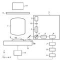
本発明にかかる位置検出方法を露光装置に適用した実施形態を説明する。図1Aは、第1実施形態にかかる露光装置の構成を示す図である。同図において、Rは電子回路パターンが形成されているレチクルであり、Wは露光基板であるウエハ、1は投影光学系である。この投影光学系1は、照明光源14より照射された投影光に基づきレチクルRの電子回路パターン像をウエハWに投影する。
<Embodiment 1>
An embodiment in which the position detection method according to the present invention is applied to an exposure apparatus will be described. FIG. 1A is a view showing the arrangement of an exposure apparatus according to the first embodiment. In the figure, R is a reticle on which an electronic circuit pattern is formed, W is a wafer as an exposure substrate, and 1 is a projection optical system. The projection optical system 1 projects an electronic circuit pattern image of the reticle R onto the wafer W based on the projection light emitted from the
Sは位置合わせ用光学系であり、照明装置、ビームスプリッタ、結像光学系、撮像手段、制御ユニットを含む。2は位置検出用の照明光を照射する位置合わせ用の照明装置であり、3はビームスプリッタ、4及び5は結像光学系である。60は照明装置2から照明された光の反射光を受光する受光時間(蓄積時間)の調節が可能な撮像手段である。16は制御ユニットであり、照明装置2が照射する光束の強度を制御したり、撮像手段60が受光する光束の受光時間を撮像評価手段12で評価した結果に基づき撮像手段60に設定したりする。撮像手段60は設定された受光時間に従って照明装置2から照明された光の反射光を受光する。
Reference numeral S denotes an alignment optical system, which includes an illumination device, a beam splitter, an imaging optical system, an imaging unit, and a control unit.
7は撮像手段60で処理された結果をデジタル信号に変換するためのA/D変換手段、8はA/D変換手段7と接続し、デジタル信号の演算が可能な積算手段であり、9はデジタル信号に基づき検出対象の位置を検出する位置検出手段である。10は照明装置2から照射された照明光の波長を切り換えるための波長切り替え手段であり、検出対象の位置計測において、位置計測用の照明光を位置検出対象に照射するにあたり、種々の波長の照明光に切り換えることが可能である。波長の切り替えは、制御ユニット16により制御することが可能である。11は2次元に移動可能なXYステージであり、13はステージ制御手段である。XYステージ11は、ウエハWの露光時において、ステージ制御手段13の制御の下に、ウエハWの被露光領域を露光するためにウエハWを移動して位置決めし、位置計測時においては、XYステージ上に載置されたウエハWの各被露光領域の位置を撮像手段60により計測するために必要なXYステージ上に設けられている基準マークSMを、撮像手段60が観察可能な範囲(WP)に位置決めすることができる。
7 is an A / D conversion means for converting the result processed by the imaging means 60 into a digital signal, 8 is an integration means which is connected to the A / D conversion means 7 and can calculate a digital signal, 9 It is a position detection means for detecting the position of the detection target based on the digital signal.
12は撮像評価手段であり、積算手段8による演算結果のばらつきを計測し、標準偏差やレンジ等の統計的な演算処理や最小二乗演算等の誤差評価に関する演算処理を行うことができる。15は位置検出手段9、撮像評価手段12において検出、評価された結果を保存するためのデータベースであり、メモリに格納された状態で書き込み、読み出しが可能である。
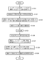
図1Bは第1実施形態における位置計測処理の流れを説明するフローチャートである。まず、ステップS101において、XYステージ11上の基準マークSMを撮像手段60の撮像画面内(WP)で観察できるように、ステージ制御手段13によりXYステージ11を駆動させて位置調整を行う。ここで、XYステージ11に設けられている基準マークSMは、ステージ上のXY平面内に図2(b)のような矩形のマークを複数配置したものである。WPは撮像手段60における撮像画面を示す観察範囲であり、ステップS101において、XYステージ11の基準マーク(SM)が撮像手段60の観察範囲(WP)内に入り、4本の基準マークを観察することができる位置に調整ができたら、処理をステップS102に進め、位置合わせ用の照明装置2から照明光を照射する。
FIG. 1B is a flowchart for explaining the flow of position measurement processing in the first embodiment. First, in step S101, the
ステップS103において、波長切り替え手段10により選択した波長の光束により、結像光学系4、ビームスプリッタ3を介して、XYステージ上の基準マークSMを照明する。基準マークSMから反射した光束は、再びビームスプリッタ3に戻り、結像光学系5を介して撮像装置60の観察範囲(WP)内に基準マークSMの像を形成する。
In step S <b> 103, the reference mark SM on the XY stage is illuminated by the light beam having the wavelength selected by the
ステップS104において、撮像装置60は基準マークSMの像を光電変換し、その後、撮像装置60からの出力は、A/D変換装置7に入力され、A/D変換装置7は光電変換の結果を2次元のデジタル信号列に変換する(S105)。撮像装置60が行う受光時間の調節により、受光量(照明光量=光束の強度×受光時間)を調節することができる。
In step S104, the
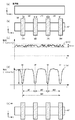
ステップS106において、積算装置8はA/D変換装置7の出力である2次元信号をY方向またはX方向に積算処理をして1次元のデジタル信号列S1(x)またはS1(y)に変換する(図2(d)はY方向に積算処理して得られたX方向のデジタル信号列の例を示す図である。)。1次元のデジタル信号列は、例えば、図2(d)に示すように基準マークSMに対応した1次元のデジタル信号列S1(x)であり、この信号列S1(x)のコントラストに基づき(例えば、当該コントラストが最大となることを条件として)撮像手段60と基準マークSMとを互いに共役な位置関係とすることができる(尚、この共役位置関係は、位置合わせ用光学系内の光学要素、撮像手段60または基準マークSMの移動等により可能である)。コントラストを求める処理は、位置検出手段9により実行させることができる。また、位置検出手段9は、積算手段8により求められた1次元のデジタル信号列S1(x)を、撮像手段60の観察範囲(WP)における位置(x)に関して微分することにより1次元のデジタル信号列S1(x)の傾きやその分布を求めたり、撮像手段60が受光した光束の強度(Intensity)の最大値や、受光した光束の強度の分布を求めたりすることができる。図2(d)において、基準マークSM1〜SM4(図2(b))の位置に対応して、信号レベルにピークが発生する(M1〜M4)。強度ピークの間隔dM1〜dM3と、基準マークの正規の配置間隔LM1〜LM3(図2(b))とを合わせることで、撮像手段60と基準マークSMとを共役位置関係にすることができる。すなわち、、撮像手段60における受光時間を変化させながら、ピーク位置M1〜M4の正規位置に対するずれのばらつき(標準偏差等)がもっとも小さくなる受光時間を求め、その受光時間で撮像手段60により撮像を行ない、得られた撮像画像のコントラストに基づき、基準マークSMと撮像手段60とを共役位置関係とすることができる。
In step S106, the
次に、位置計測用として選択した波長毎の照射光によるちらつきや電気的なノイズの影響を求める。まず、ステップS107において、基準マークやパターンのない計測用の領域を位置計測用の照明により照射するために、図2(a)のように観察できる領域(基準マークSMが存在していないXYステージ上の計測領域(以下、「基準面」ともいう。))を、撮像手段60の撮像画面(WP)内で観察できるように位置調整する。そして、この基準面に対して、先に説明した基準マークSMに対する処理と同様に、選択した波長の光束で照射し、その反射光をビームスプリッタ3、結像光学系5を介して撮像手段60で受光して、基準面からの反射像に関する光電変換を行う。そして、撮像手段60による光電変換の結果は、その後、A/D変換器7によりA/D変換され、基準面に対する1次元のデジタル信号列が求められる。このようにして、撮像手段60における受光時間tc毎に、基準マークSMに関する1次元のデジタル信号列と、基準面に関する1次元のデジタル信号列との相対的な関係(S/N比)を求めることができる。
Next, the influence of the flicker and electrical noise caused by the irradiation light for each wavelength selected for position measurement is obtained. First, in step S107, in order to irradiate a measurement area without a reference mark or pattern with illumination for position measurement, an area that can be observed as shown in FIG. 2A (an XY stage in which no reference mark SM is present). The position of the upper measurement region (hereinafter also referred to as “reference plane”) is adjusted so that it can be observed in the imaging screen (WP) of the imaging means 60. Then, similar to the processing for the reference mark SM described above, the reference surface is irradiated with a light beam having a selected wavelength, and the reflected light is imaged through the
ここで、図2(c)は、1次元のデジタル信号列として、X方向における1次元のデジタル信号列So(x)を例示する図である。So(x)の分布より、パターンや基準マークのない基準面を観測した場合、位置合わせ用の照明装置2の光源のちらつきや撮像装置の電気的特性により、デジタル信号列は一様ではなく、図2(c)のようにばらついていることがわかる。そこで、このばらつき(例えば標準偏差)を撮像評価手段12で求め、このばらつきに基づき最適な受光時間を決定する(S109)。ここで決定された受光時間は、制御ユニット16が撮像手段60に設定する。
Here, FIG. 2C is a diagram illustrating a one-dimensional digital signal sequence So (x) in the X direction as the one-dimensional digital signal sequence. When a reference plane having no pattern or reference mark is observed from the distribution of So (x), the digital signal sequence is not uniform due to the flickering of the light source of the
ここで、最適な受光時間を決定する具体的な処理としては、例えば、図3Aのように横軸に撮像手段60における受光時間tciをとり、縦軸に基準面での反射光に基づく1次元デジタル信号列のばらつき(標準偏差やレンジなど、撮像評価手段12により得られたばらつきの指標となる値)をとり(図3Aでは縦軸に標準偏差をとった例を示している。)、両者の関係から1次元デジタル信号列のばらつきがもっとも小さくなるような受光時間tciminを求めるものである。受光時間tciminは、図3Aに示すように受光時間を変化させながら標準偏差を求め、標準偏差の値がもっとも小さくなる受光時間として特定することができる。この受光時間tciminは位置計測用の照明装置2の光源のちらつきや撮像手段60の電気的特性によるばらつきの影響を最も小さくすることを可能にする受光時間であり、撮像手段60によりこの受光時間でアライメントマークを撮像すれば、S/N比を最も高くすることができる。
Here, as a specific process for determining the optimum light reception time, for example, as shown in FIG. 3A, the horizontal axis represents the light reception time tci in the imaging means 60, and the vertical axis represents one-dimensional based on the reflected light on the reference plane. Variations of the digital signal sequence (standard deviation, range, and other values used as an index of variation obtained by the imaging evaluation means 12) are taken (in FIG. 3A, the vertical axis shows the standard deviation), and both. From this relationship, the light reception time tcimin that minimizes the variation in the one-dimensional digital signal sequence is obtained. As shown in FIG. 3A, the light reception time tcimin can be specified as the light reception time in which the standard deviation is obtained by obtaining the standard deviation while changing the light reception time. This light reception time tcimin is a light reception time that makes it possible to minimize the influence of the flickering of the light source of the
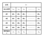
以上の処理を波長切り替え手段10で切り換えることが可能な照明光の波長λiすべてに関して実行し、基準面1次元デジタル信号列のばらつきが最も小さくなるような受光時間tciminを波長λi毎に求める。図3Bは波長切り換え手段10により切り換えられる照明光の各波長λiと、受光時間tciminとの関係を示す図である。選択した波長に応じて、受光時間tciminを切り換えることで、照明光のちらつき等の影響を低減することができ、撮像手段60の受光光量をS/N比が最も高くなるように調整することができる。
The above processing is executed for all wavelengths λi of illumination light that can be switched by the wavelength switching means 10, and a light reception time tcimin that minimizes the variation in the reference plane one-dimensional digital signal sequence is obtained for each wavelength λi. FIG. 3B is a diagram showing the relationship between each wavelength λi of the illumination light switched by the wavelength switching means 10 and the light reception time tcimin. By switching the light reception time tcimin according to the selected wavelength, the influence of flickering of illumination light and the like can be reduced, and the amount of light received by the
図3Bの波長と受光時間との関係は、例えば、メモリ内のデータベース15にルックアップテーブル(LUT)として格納され、露光装置によるウエハWに対するアライメント計測の際、このLUTを参照することにより、選択した波長に応じた受光時間で位置計測を実行することができる。
The relationship between the wavelength and the light reception time in FIG. 3B is selected by referring to this LUT when the alignment measurement is performed on the wafer W by the exposure apparatus, for example, stored as a look-up table (LUT) in the
尚、本実施形態において、図2(c)、(d)で示した1次元のデジタル信号列はX軸方向に関するものであったが、Y軸方向のデジタル信号列を用いてももよく、また、当該方向ごとにまたは両方向の信号列のデータに基づき受光時間(tcimin)を決定するようにしてもよい。 In this embodiment, the one-dimensional digital signal sequence shown in FIGS. 2C and 2D is related to the X-axis direction, but a digital signal sequence in the Y-axis direction may be used. In addition, the light reception time (tcimin) may be determined for each direction or based on data of signal strings in both directions.
<実施形態2>
第1実施形態では最適な受光時間tcを求めるために、XYステージ11に設けられた基準マークSMと、基準マークのない面(基準面)とを観察したときの1次元のデジタル信号列のデータに基づいて最小の受光時間(tcimin)を決定していたが、本実施形態では、基準マークSMの位置計測結果のみを指標に最適な受光時間を求める。本実施形態において、XYステージ11における基準マークSMに対する1次元のデジタル信号列に基づいて撮像手段60と基準マークSMとを共役位置関係に調整する処理(図1BのステップS101〜S106)は、第1実施形態と同様に行うものとする。
<
In the first embodiment, in order to obtain an optimum light receiving time tc, data of a one-dimensional digital signal sequence when a reference mark SM provided on the
図1Cは、図1BのステップS106に後続する第2実施形態の具体的な処理の流れを説明するフローチャートである。まず、ステップS201において、位置計測手段9を用いて図2(d)に示す基準マークSMの信号に基づき各矩形マークの位置M1〜M4を計測し、ステップS202において、各矩形マーク間の距離(スパン)dM1〜dM4を求める。ここで、各矩形マーク間のスパンdM1(=M2−M1)〜dM4(=M4−M1)のばらつきは、照明装置2の光源のちらつきや撮像装置60の電気的特性などの要因で起こるものである。撮像手段60における受光時間を変化させながら、基準マークSMにおける矩形マーク間のスパンdM1〜dM4を計測し、計測結果に基づきスパンのばらつきを撮像評価手段12が逐次演算する。図3Cは、ある波長λ1の光束に関し、受光時間をtc1、tc2、tc3、・・・tcmと変化させた場合のスパンdM1〜dM4の計測結果をデータテーブルとしてまとめた図であり、各受光時間毎にスパンdM1〜dM4の標準偏差(σ)が求められる。また、図2(b)に示すように矩形マーク間の規範長さとしてLM1〜LM4が既知な量として定められている場合には、この規範長さ(LMi)と、計測したマークスパン(dMi)との差分に関して標準偏差等を求めてもよい(ステップS203)。尚、統計的な指標としては、標準偏差の他、計測値の最大値と最小値の幅としてのレンジや最小二乗法を用いて求めた規範長さ(LMi)と計測値(dMi)との関係(例えば、当該関係を示す近似直線の傾き等のパラメータ)であってもよい。これらの統計的指標を撮像手段60が反射光を受光する受光時間を変化させながら求める。そして、ステップS204において、ステップS203で求めた統計的指標に基づいて(例えば、マークスパンdM1〜dM4に関する標準偏差やレンジ等を最小にする受光時間を最適なものとして)受光時間を決定する。そして、ここで決定された受光時間は、制御ユニット16が撮像手段60に設定する。
FIG. 1C is a flowchart for explaining a specific processing flow of the second embodiment subsequent to step S106 of FIG. 1B. First, in step S201, the position measuring means 9 is used to measure the positions M1 to M4 of each rectangular mark based on the signal of the reference mark SM shown in FIG. 2D, and in step S202, the distance between the rectangular marks ( Span) dM1 to dM4 are obtained. Here, variations in spans dM1 (= M2-M1) to dM4 (= M4-M1) between the rectangular marks are caused by factors such as flickering of the light source of the
最適な受光時間を決定するには、たとえば、第1実施形態で説明した図3Aのように、横軸に撮像手段60における受光時間tciをとり、縦軸にマークスパンdM1〜dM4に関する標準偏差やレンジなど、撮像評価手段12により得られた1次元デジタル信号列のばらつきを示すデータをとり、1次元デジタル信号列のばらつきがもっとも小さくなるような受光時間tciminを求めればよい。このようにして得られた受光時間tciminは、位置計測用の照明装置2の光源のちらつきや撮像装置の電気的特性によるばらつきの影響を最も小さくする受光時間である。尚、位置計測手段9により、位置検出用に切り換えられる光束の波長毎に、受光時間tciminを求めるようにする。また、波長と受光時間との関係は、第1実施形態において説明したLUT(図3B)と同様に、アライメント計測時において参照可能な状態でメモリ内のデータベース15に格納される。
In order to determine the optimum light reception time, for example, as shown in FIG. 3A described in the first embodiment, the horizontal axis represents the light reception time tci in the
実際にアライメントマークを計測するときは、計測時の照明波長にあわせて受光時間tciminを変更し、アライメントマークを撮像する。選択した波長に応じて、受光時間tciminを切り換えることで、照明光のちらつき等の影響を排除することができ、また、撮像手段60の受光光量に関し、S/N比を最も高くするように調整することができる。よって、位置計測用の照明光の波長を切り換えた場合でも、波長または波長に対応した光源によらずS/N比の良好な画像ことができる。 When actually measuring the alignment mark, the light reception time tcimin is changed in accordance with the illumination wavelength at the time of measurement, and the alignment mark is imaged. By switching the light reception time tcimin according to the selected wavelength, it is possible to eliminate the influence of flickering of illumination light and the like, and the S / N ratio is adjusted to be the highest with respect to the amount of light received by the imaging means 60. can do. Therefore, even when the wavelength of the illumination light for position measurement is switched, an image with a good S / N ratio can be obtained regardless of the wavelength or the light source corresponding to the wavelength.
本実施形態では、基準マークSMの撮像信号における各矩形マークの間隔(スパン)の「ばらつき」を最小にする受光時間を決定したが、撮像の対象は、XYステージ11上の基準マークSMに限定されず、例えば、露光の対象となるウエハW上に設けられたウエハマークWM(図1A)であってもよい。ウエハマークWMを照明装置2により照明し得られた撮像結果に基づき、ウエハマークWMの間隔のばらつきを最小にするものとして受光時間tciminを決定することも可能である。ウエハW上のマークWMを計測に使用するとともに、本実施形態の処理をウエハW枚葉に適用すれば、ウエハ毎にウエハ表面状態やマーク形状がばらついていても、それぞれのウエハにおいて最適な受光時間tciminを決定することが可能になる。
In the present embodiment, the light receiving time that minimizes the “variation” of the interval (span) between the rectangular marks in the imaging signal of the reference mark SM is determined. However, the imaging target is limited to the reference mark SM on the
ウエハマークWMを基準とする場合、計測対象マークすべてに関して最適な受光時間tciminを求めてもよいが、その場合処理に長時間を要することになるので、例えば、代表的なウエハマークWM(例えば、1つのサンプルショットに対応して設けられたウエハマーク)に関して最適な受光時間を求め、他のウエハマークに関しては代表的なウエハマークで求めた受光時間で撮像するようにして、受光時間を求める処理時間を短縮することも可能である。また、ロット内でウエハ表面状態やウエハマークの形状が安定している場合は、ロット内の第1ウエハで求めた最適な受光時間tciminを、以降の同一ロット内のウエハで使用することも可能である。 When the wafer mark WM is used as a reference, the optimum light receiving time tcimin may be obtained for all the measurement target marks. In this case, however, the processing takes a long time. For example, a representative wafer mark WM (for example, A process for obtaining a light reception time by obtaining an optimum light reception time for a wafer mark provided corresponding to one sample shot and imaging for the other wafer marks with a light reception time obtained by a typical wafer mark. It is also possible to shorten the time. In addition, when the wafer surface condition and wafer mark shape are stable in the lot, the optimum light receiving time tcimin obtained for the first wafer in the lot can be used for the subsequent wafers in the same lot. It is.
以上のように、波長切り換え手段10により切り換えられた照明波長に最適な受光時間とすることにより、より高精度なアライメントマークの位置計測が可能となる。また、ウエハW上のマークの撮像データを指標として受光時間を決定することにより、実際のウエハに最適な受光時間を決定することができる。 As described above, it is possible to measure the position of the alignment mark with higher accuracy by setting the light reception time optimal for the illumination wavelength switched by the wavelength switching means 10. In addition, by determining the light reception time using the imaging data of the mark on the wafer W as an index, it is possible to determine the optimal light reception time for an actual wafer.
<実施形態3>
第2実施形態では、最適な受光時間を求めるために、基準マークSMまたはウエハマークWMの撮像信号におけるマークスパンのばらつきを指標としていたが、本実施形態ではXYステージに設けられた基準マークSMの計測位置のばらつきを指標として最適な受光量(受光時間)を決定する。本実施形態において、撮像手段60と基準マークSMとを共役位置関係に調整する処理(図1BのステップS101〜S106)は、第1実施形態と同様に実行される。
<
In the second embodiment, in order to obtain the optimum light receiving time, the mark span variation in the imaging signal of the reference mark SM or the wafer mark WM is used as an index. However, in this embodiment, the reference mark SM provided on the XY stage is used as an index. The optimum amount of received light (light reception time) is determined using the variation in measurement position as an index. In the present embodiment, the process (steps S101 to S106 in FIG. 1B) for adjusting the
図1Dは、図1BのステップS106に後続する第3実施形態の具体的な処理の流れを説明するフローチャートである。まず、ステップS301において、位置計測手段9を用いて、図2(d)に示す基準マークSMの撮像信号に基づき、各矩形マークの中央位置に対応するピークの位置M1〜M4を計測する。ここで、位置M1〜M4の各基準位置(各矩形マークの設計上または実際の位置)に対するばらつきは照明光源のちらつきや撮像手段60の電気的特性、さらにはステージやステージの位置を計測する干渉計などの要因で起こるものである。ピークの位置M1〜M4は、基準マークSMを撮像した際に得られる1次元のデジタル信号列S1(x)において、例えば、図2(d)のピークの位置として求めることができる。 FIG. 1D is a flowchart for explaining a specific processing flow of the third embodiment subsequent to step S106 of FIG. 1B. First, in step S301, the position measuring means 9 is used to measure the peak positions M1 to M4 corresponding to the center position of each rectangular mark based on the imaging signal of the reference mark SM shown in FIG. Here, the variation of each of the positions M1 to M4 with respect to each reference position (designed or actual position of each rectangular mark) is flickering of the illumination light source, electrical characteristics of the imaging means 60, and interference for measuring the stage and the position of the stage. This is caused by factors such as totals. The peak positions M1 to M4 can be obtained, for example, as the peak positions in FIG. 2D in the one-dimensional digital signal sequence S1 (x) obtained when the reference mark SM is imaged.
ステップS302において、撮像手段60における受光時間を変えながら、計測位置M1〜M4のばらつき(標準偏差等)を求める。尚、ばらつきの統計的な指標としては、第2実施形態と同様に、標準偏差の他、最大値と最小値との差としてのレンジ等を使用してもよい。
In step S302, the variation (standard deviation or the like) of the measurement positions M1 to M4 is obtained while changing the light reception time in the
そして、ステップ303において、ステップS302で求めた位置M1〜M4のばらつき(標準偏差やレンジ等)に基づき、(標準偏差等のばらつきの指標を最小にするものとして)受光時間を決定する。ここで決定された受光時間は、制御ユニット16が撮像手段60に設定する。
In step 303, based on the variation (standard deviation, range, etc.) of the positions M1 to M4 obtained in step S302, the light reception time is determined (assuming that the variation index such as standard deviation is minimized). The light receiving time determined here is set in the imaging means 60 by the
最適な受光時間を決定するには、たとえば、第1実施形態で説明した図3Aのように、横軸に撮像手段60における受光時間tciをとり、縦軸に計測値M1〜M4に関する標準偏差やレンジなど、撮像評価手段12により得られたばらつきの指標をとり、計測値M1〜M4のばらつきがもっとも小さくなるような受光時間tciminを求めればよい。この受光時間tciminは位置計測用の照明装置2の光源のちらつきや撮像装置の電気的特性等によるばらつきの影響を最も小さくする受光時間である。また、位置計測手段9により、位置検出用に切り換えられる光束の波長毎に、受光時間tciminを求めるようにする。波長と受光時間の関係は、第1実施形態において説明したLUT(図3B)のように、アライメント計測時において参照可能な状態でメモリ内のデータベース15に格納される。
In order to determine the optimum light receiving time, for example, as shown in FIG. 3A described in the first embodiment, the horizontal axis represents the light receiving time tci in the imaging means 60, and the vertical axis represents the standard deviation regarding the measured values M1 to M4. The light reception time tcimin that minimizes the variation of the measured values M1 to M4 may be obtained by taking the variation index obtained by the
実際にアライメントマークを計測するときは、計測時の照明波長にあわせて受光時間tciminを変更し、アライメントマークを撮像する。選択した波長に応じて、受光時間tciminを切り換えることで、照明光のちらつき等の影響を排除することができ、撮像手段60の受光光量に関し、S/N比を最も高くするように調整することができる。よって、波長または波長に対応した光源によらずにS/N比の良好な画像を得ることができる。 When actually measuring the alignment mark, the light reception time tcimin is changed in accordance with the illumination wavelength at the time of measurement, and the alignment mark is imaged. By switching the light reception time tcimin according to the selected wavelength, the influence of flickering of illumination light and the like can be eliminated, and the S / N ratio is adjusted to be the highest with respect to the amount of light received by the imaging means 60. Can do. Therefore, an image having a good S / N ratio can be obtained regardless of the wavelength or the light source corresponding to the wavelength.
本実施形態では、基準マークSMの撮像信号における各矩形マークの位置の「ばらつき」を最小にする受光時間を決定したが、撮像の対象は、XYステージ11上の基準マークSMに限定されず、例えば、露光の対象となるウエハW上に設けられたウエハマークWM(図1A)であってもよい。ウエハマークWMを計測に使用にするとともに、ウエハWに対し枚葉で本実施形態の処理を適用することにより、ウエハ毎にウエハ表面状態やマーク形状がばらついていても、それぞれのウエハにおいて最適な受光時間tciminを決定することが可能になる。
In this embodiment, the light receiving time that minimizes the “variation” of the position of each rectangular mark in the imaging signal of the reference mark SM is determined, but the imaging target is not limited to the reference mark SM on the
また、ウエハ上の計測マークすべてに関し最適な受光時間tciminを求めてもよいが、個別に受光時間を求める場合は処理に長時間を要することになるので、例えば、代表的な1つのウエハマークWM(例えば、1つのサンプルショットに対応して設けられたウエハマーク)に関して最適な受光時間を求め、他のウエハマークに関しては代表的なウエハマークWMで求めた受光時間で撮像するようにして、受光時間を決める処理時間を短縮することも可能である。また、ロット内でウエハ表面状態やウエハマークの形状が安定している場合は、ロット内の第1ウエハで求めた最適な受光時間tciminを、以降の同一ロット内のウエハに適用することも可能である。 Further, the optimum light receiving time tcimin may be obtained for all the measurement marks on the wafer. However, when the light receiving time is obtained individually, it takes a long time to process, for example, one representative wafer mark WM. For example, an optimum light receiving time is obtained with respect to (for example, a wafer mark provided corresponding to one sample shot), and the other wafer marks are picked up with a light receiving time obtained with a representative wafer mark WM. It is also possible to shorten the processing time for determining the time. In addition, when the wafer surface condition and the shape of the wafer mark are stable in the lot, the optimum light receiving time tcimin obtained for the first wafer in the lot can be applied to the subsequent wafers in the same lot. It is.
以上のように、波長切り換え手段10により切り換えられた照明波長に最適な受光時間とすることにより、より高精度なアライメントマークの位置計測が可能となる。また、ウエハW上のマークの撮像信号に基づいて受光時間を決定することにより、実際のウエハに最適な受光時間を決定することができる。 As described above, it is possible to measure the position of the alignment mark with higher accuracy by setting the light reception time optimal for the illumination wavelength switched by the wavelength switching means 10. Further, by determining the light reception time based on the image pickup signal of the mark on the wafer W, it is possible to determine the optimal light reception time for the actual wafer.
また、上述の受光時間の決定において、ステージの振動や、干渉計の計測誤差の影響も加味してマークの位置を評価する(例えば、受光時間中の複数のステージ位置データに基づき(例えば、ステージ位置を当該複数の位置の平均的な位置として)マーク位置を求める)ことにより、光源のちらつきや撮像手段60の電気的特性・ノイズのみならず、XYステージ11の振動や、レーザ干渉計(不図示)の計測誤差の影響をも排除することが可能になる。
Further, in the determination of the light reception time described above, the position of the mark is evaluated in consideration of the stage vibration and the measurement error of the interferometer (for example, based on a plurality of stage position data during the light reception time (for example, the stage By calculating the mark position (with the position as an average position of the plurality of positions), not only the flickering of the light source and the electrical characteristics / noise of the imaging means 60 but also the vibration of the
<実施形態4>
上述の第2、第3実施形態では、基準マークSMを構成する矩形マークの間隔(スパン)や矩形マークの計測位置から最適な受光時間を求めたが、計測精度を確保できる光量トレランスを求めることも可能である。
<
In the second and third embodiments described above, the optimum light reception time is obtained from the interval (span) of the rectangular marks constituting the reference mark SM and the measurement position of the rectangular marks. However, the light amount tolerance that can ensure the measurement accuracy is obtained. Is also possible.
光量トレランスとは、基準マークSMやウエハマークWMの撮像において、撮像手段60の受光量が計測に適したレベルであるかどうかの判定基準である。光量トレランスを設定し基準マーク等の位置計測時に受光量がこの光量トレランスの範囲内になるように受光時間や照明強度の調整を行うことにより、受光時間を調整するための時間の短縮が可能になる。以下、光量トレランスを求めるための手順を説明する。
The light amount tolerance is a criterion for determining whether or not the amount of light received by the
本実施形態において、撮像手段60と基準マークSMとを共役位置関係に調整する処理(図1BのステップS101〜S106)は、第1実施形態と同様に実行される。
In the present embodiment, the process (steps S101 to S106 in FIG. 1B) for adjusting the
図1Eは、図1BのステップS106に後続する第4実施形態の具体的な処理の流れを説明するフローチャートである。まず、ステップS401において、位置計測手段9を用いて、図2(d)に示す基準マークSMの撮像信号における各矩形マークの位置M1〜M4を計測し、ステップS402において、当該計測結果に基づいて、各矩形マーク間のスパンdM1(=M2−M1)、dM2(=M3−M2)、dM3(=M4−M3)、dM4(=M4−M1)を求める。 FIG. 1E is a flowchart for explaining a specific processing flow of the fourth embodiment subsequent to step S106 of FIG. 1B. First, in step S401, the position measuring means 9 is used to measure the positions M1 to M4 of each rectangular mark in the image signal of the reference mark SM shown in FIG. 2D, and in step S402, based on the measurement result. The spans dM1 (= M2-M1), dM2 (= M3-M2), dM3 (= M4-M3), and dM4 (= M4-M1) between the rectangular marks are obtained.
ここで、各矩形マーク間のスパンdM1〜dM4のばらつきは、先の実施形態でも説明したとおり、照明装置2の光源のちらつきや撮像装置60の電気的特性などの要因で起こるものである。
Here, the variations in the spans dM1 to dM4 between the rectangular marks are caused by factors such as flickering of the light source of the
ステップS403において、求めたスパンdM1〜dM4のばらつき(標準偏差等)を、光束の波長、撮像手段60の受光時間、照明強度を変化させながら、撮像評価手段12により逐次演算させる。この結果は第2実施形態で説明したように、例えば,図4Bのようなデータテーブルにまとめられ、データベース15に格納される。図4Bは、位置計測に用いられる光束の波長をλiとし、受光量Hi(照明強度I、撮像手段60の受光時間Tcにより決まる)を変えた場合のマークスパンdM1〜dM4の計測結果と、そのときの標準偏差との関係をテーブル形式にまとめた図である。ここで、波長λi毎に許容標準偏差σaiを定めている。この許容標準偏差σaiは、許容されるばらつきの最大値を示すデータである。
In step S403, the
ステップS404において、ステップS403の演算結果に基づいて最適な光量トレランスを決定する。最適な光量トレランスを決定する具体的な処理としては、たとえば、図4Aに示すように、横軸に受光量、縦軸にマークスパンの標準偏差をとり、許容標準偏差σaiを与える受光量を光量トレランスの下限とする。図4Aにおいて、斜線で示す部分は、許容標準偏差σai以下のばらつきを与える受光量の範囲となる。この範囲が光量トレランスである。一般的に受光量は撮像手段60やA/D変換手段7のダイナミックレンジ内でできるだけ大きなほうがよいが、矩形マークの位置計測精度に悪影響を与えない範囲内(光量トレランス内)ならば小さくてもかまわない。 In step S404, an optimum light amount tolerance is determined based on the calculation result of step S403. As a specific process for determining the optimum light amount tolerance, for example, as shown in FIG. 4A, the received light amount giving the allowable standard deviation σai with the received light amount on the horizontal axis and the standard deviation of the mark span on the vertical axis. The lower limit of tolerance. In FIG. 4A, the hatched portion is a range of received light amount that gives a variation of the allowable standard deviation σai or less. This range is the light amount tolerance. In general, the received light amount should be as large as possible within the dynamic range of the image pickup means 60 and the A / D conversion means 7, but may be small if it is within a range that does not adversely affect the position measurement accuracy of the rectangular mark (within the light amount tolerance). It doesn't matter.
図4Aは所定の波長λiに関して標準偏差と受光量の関係を示す図であり、上述の処理を波長切り替え手段10で設定可能な照明波長のそれぞれに関して実行し、照明波長毎にマークスパンdM1〜dM4の標準偏差が所定の許容標準偏差以下になることを条件として光量トレランスを求める(S401〜S404)。 FIG. 4A is a diagram showing the relationship between the standard deviation and the amount of received light with respect to a predetermined wavelength λi. The above processing is executed for each of the illumination wavelengths that can be set by the wavelength switching means 10, and the mark spans dM1 to dM4 for each illumination wavelength. The light quantity tolerance is obtained on the condition that the standard deviation of the light becomes equal to or smaller than a predetermined allowable standard deviation (S401 to S404).
実際にアライメントマークを計測するときは、計測時の照明波長λiに応じて、上述のようにしてに求めた光量トレランス内の受光量Hiに切り換えることにより、照明光のちらつき等の影響を排除することができ、撮像手段60の受光光量に関し、許容できるS/N比を確保できるように調整することができる。よって、波長または波長に対応した光源によらずS/N比の良好な画像を得ることができる。尚、受光量は、照射する光束の強度と撮像手段60の受光時間とにより決まるため、制御ユニット16は、そのどちらか一方あるいは両方のパラメータを調整することにより、上述の光量トレランスの条件を満たすように、照明手段2および/または撮像手段60を制御する。
When the alignment mark is actually measured, the influence of flickering of illumination light and the like is eliminated by switching to the received light amount Hi within the light amount tolerance obtained as described above according to the illumination wavelength λi at the time of measurement. The amount of light received by the imaging means 60 can be adjusted to ensure an acceptable S / N ratio. Therefore, an image having a good S / N ratio can be obtained regardless of the wavelength or the light source corresponding to the wavelength. Since the amount of received light is determined by the intensity of the irradiated light beam and the light receiving time of the image pickup means 60, the
また、本実施形態では基準マークSMの矩形マークのスパンのばらつきに基づき光量トレランスを決定したが、ウエハ上のマークWMの矩形マークのスパンに基づき光量トレランスを決定することも可能である。この場合、ウエハ上のマークWMを使用するとともに、ウエハWに対し枚葉で本実施形態の処理を適用することにより、ウエハ毎にウエハ表面状態やマーク形状がばらついていても、それぞれのウエハに応じた光量トレランスを決定することが可能になる。ウエハ上のマーク毎に光量トレランスを求めてもよいが、ウエハ上の代表的なマーク(例えば、1つのサンプルショット領域に対応して設けられたマーク)により光量トレランスを求め、他のマークに関しては上記代表マークに関し求めた光量トレランスを使用すれば、光量トレランスを求める処理時間を短縮することができる。また、ロット内の第1ウエハに関して求めた光量トレランスを以降の同一ロット内のウエハに関して使用することも可能である。 In this embodiment, the light amount tolerance is determined based on the variation of the span of the rectangular mark of the reference mark SM. However, the light amount tolerance can also be determined based on the span of the rectangular mark of the mark WM on the wafer. In this case, by using the mark WM on the wafer and applying the processing of the present embodiment to the wafer W as a single wafer, even if the wafer surface state and the mark shape vary from wafer to wafer, It becomes possible to determine the light amount tolerance according to the above. The light amount tolerance may be obtained for each mark on the wafer, but the light amount tolerance is obtained from a representative mark on the wafer (for example, a mark provided corresponding to one sample shot area), and other marks are related. If the light quantity tolerance obtained for the representative mark is used, the processing time for obtaining the light quantity tolerance can be shortened. It is also possible to use the light amount tolerance obtained for the first wafer in the lot for the subsequent wafers in the same lot.
このように照明波長毎に予め求めた光量トレランスの条件を満たすように受光量を制御することにより、より高精度なアライメントマークの位置計測が可能となる。また、また、ウエハW上のマークの撮像データに基づいて光量トレランスを決定することにより、実際のウエハに最適な光量トレランスを決定することができる。 In this way, by controlling the amount of received light so as to satisfy the light amount tolerance obtained in advance for each illumination wavelength, the position of the alignment mark can be measured with higher accuracy. Further, by determining the light amount tolerance based on the imaging data of the mark on the wafer W, it is possible to determine the optimum light amount tolerance for the actual wafer.
<デバイス製造方法の実施形態>
次に上記の露光装置を利用した半導体デバイスの製造プロセスを説明する。図6は、半導体デバイスの全体的な製造プロセスのフローを示す図である。ステップ1(回路設計)では半導体デバイスの回路設計を行なう。ステップ2(マスク作製)では設計した回路パターンに基づいてマスクを作製する。一方、ステップ3(ウエハ製造)ではシリコン等の材料を用いてウエハを製造する。ステップ4(ウエハプロセス)は前工程と呼ばれ、上記のマスクとウエハを用いて、リソグラフィ技術によってウエハ上に実際の回路を形成する。次のステップ5(組み立て)は後工程と呼ばれ、ステップ4によって作製されたウエハを用いて半導体チップ化する工程であり、アッセンブリ工程(ダイシング、ボンディング)、パッケージング工程(チップ封入)等の組み立て工程を含む。ステップ6(検査)ではステップ5で作製された半導体デバイスの動作確認テスト、耐久性テスト等の検査を行なう。こうした工程を経て半導体デバイスが完成し、これを出荷(ステップ7)する。
<Embodiment of Device Manufacturing Method>
Next, a semiconductor device manufacturing process using the above exposure apparatus will be described. FIG. 6 is a diagram showing a flow of an entire manufacturing process of a semiconductor device. In step 1 (circuit design), a semiconductor device circuit is designed. In step 2 (mask fabrication), a mask is fabricated based on the designed circuit pattern. On the other hand, in step 3 (wafer manufacture), a wafer is manufactured using a material such as silicon. Step 4 (wafer process) is called a pre-process, and an actual circuit is formed on the wafer by lithography using the mask and wafer. The next step 5 (assembly) is called a post-process, and is a process for forming a semiconductor chip using the wafer produced in
図7は、上記ウエハプロセスの詳細なフローを示す図である。ステップ11(酸化)ではウエハの表面を酸化させる。ステップ12(CVD)ではウエハ表面に絶縁膜を成膜する。ステップ13(電極形成)ではウエハ上に電極を蒸着によって形成する。ステップ14(イオン打込み)ではウエハにイオンを打ち込む。ステップ15(レジスト処理)ではウエハに感光剤を塗布する。ステップ16(露光)では上記の露光装置によって回路パターンをウエハに転写する。ステップ17(現像)では露光したウエハを現像する。ステップ18(エッチング)では現像したレジスト像以外の部分を削り取る。ステップ19(レジスト剥離)ではエッチングが済んで不要となったレジストを取り除く。これらのステップを繰り返し行なうことによって、ウエハ上に多重に回路パターンを形成する。 FIG. 7 shows a detailed flow of the wafer process. In step 11 (oxidation), the wafer surface is oxidized. In step 12 (CVD), an insulating film is formed on the wafer surface. In step 13 (electrode formation), an electrode is formed on the wafer by vapor deposition. In step 14 (ion implantation), ions are implanted into the wafer. In step 15 (resist process), a photosensitive agent is applied to the wafer. In step 16 (exposure), the circuit pattern is transferred onto the wafer by the exposure apparatus described above. In step 17 (development), the exposed wafer is developed. In step 18 (etching), portions other than the developed resist image are removed. In step 19 (resist stripping), unnecessary resist after etching is removed. By repeating these steps, multiple circuit patterns are formed on the wafer.
Claims (27)
撮像手段と、
前記撮像手段により得られた画像データのばらつきを求める演算手段と、
異なる受光量で前記撮像手段により得られた複数の画像データに関し前記演算手段によりそれぞれ求めたばらつきに基づき、前記撮像手段の受光量に関するパラメータを設定する設定手段と
を備えたことを特徴とする位置計測装置。 A position measuring device for measuring the position of a mark,
Imaging means;
Arithmetic means for obtaining variations in image data obtained by the imaging means;
And a setting means for setting a parameter relating to the amount of received light of the imaging means based on variations respectively obtained by the calculating means for a plurality of image data obtained by the imaging means with different amounts of received light. Measuring device.
請求項1に記載の位置計測装置を備えた
ことを特徴とする露光装置。 An exposure apparatus for exposing a pattern to a substrate,
An exposure apparatus comprising the position measuring apparatus according to claim 1.
撮像手段により撮像する撮像工程と、
撮像工程において得られた画像データのばらつきを求める演算工程と、
前記撮像工程において異なる受光量で得られた複数の画像データに関し前記演算工程においてそれぞれ求めたばらつきに基づき、前記撮像手段の受光量に関するパラメータを設定する設定工程と
を備えたことを特徴とする位置計測方法。 A position measurement method for measuring the position of a mark,
An imaging step of imaging by imaging means;
A calculation step for obtaining variations in image data obtained in the imaging step;
A setting step for setting a parameter relating to the amount of received light of the imaging means based on variations obtained in the calculation step for a plurality of image data obtained at different amounts of received light in the imaging step. Measurement method.
Priority Applications (5)
| Application Number | Priority Date | Filing Date | Title |
|---|---|---|---|
| JP2004106361A JP3880589B2 (en) | 2004-03-31 | 2004-03-31 | Position measuring apparatus, exposure apparatus, and device manufacturing method |
| US11/085,545 US7126670B2 (en) | 2004-03-31 | 2005-03-22 | Position measurement technique |
| TW094109650A TWI282044B (en) | 2004-03-31 | 2005-03-28 | Position measurement technique |
| CNB2005100627748A CN100394573C (en) | 2004-03-31 | 2005-03-30 | Position measurement technique |
| KR1020050026866A KR100671350B1 (en) | 2004-03-31 | 2005-03-31 | Position measurement technology |
Applications Claiming Priority (1)
| Application Number | Priority Date | Filing Date | Title |
|---|---|---|---|
| JP2004106361A JP3880589B2 (en) | 2004-03-31 | 2004-03-31 | Position measuring apparatus, exposure apparatus, and device manufacturing method |
Publications (2)
| Publication Number | Publication Date |
|---|---|
| JP2005294474A true JP2005294474A (en) | 2005-10-20 |
| JP3880589B2 JP3880589B2 (en) | 2007-02-14 |
Family
ID=35050052
Family Applications (1)
| Application Number | Title | Priority Date | Filing Date |
|---|---|---|---|
| JP2004106361A Expired - Fee Related JP3880589B2 (en) | 2004-03-31 | 2004-03-31 | Position measuring apparatus, exposure apparatus, and device manufacturing method |
Country Status (5)
| Country | Link |
|---|---|
| US (1) | US7126670B2 (en) |
| JP (1) | JP3880589B2 (en) |
| KR (1) | KR100671350B1 (en) |
| CN (1) | CN100394573C (en) |
| TW (1) | TWI282044B (en) |
Cited By (2)
| Publication number | Priority date | Publication date | Assignee | Title |
|---|---|---|---|---|
| JP2008147206A (en) * | 2006-12-05 | 2008-06-26 | Canon Inc | Exposure apparatus and device manufacturing method |
| JP2008281391A (en) * | 2007-05-09 | 2008-11-20 | Pulstec Industrial Co Ltd | Three-dimensional shape measuring apparatus and three-dimensional shape measuring method |
Families Citing this family (10)
| Publication number | Priority date | Publication date | Assignee | Title |
|---|---|---|---|---|
| US7085677B1 (en) * | 2004-04-19 | 2006-08-01 | Amazon Technologies, Inc. | Automatically identifying incongruous item packages |
| JP2006269497A (en) * | 2005-03-22 | 2006-10-05 | Olympus Corp | Substrate processing apparatus and substrate storage method |
| US8195792B2 (en) * | 2009-01-16 | 2012-06-05 | Microsoft Corporation | Interfacing distinct services for providing web based document manipulation access |
| JP5460662B2 (en) * | 2011-09-07 | 2014-04-02 | 株式会社日立ハイテクノロジーズ | Region determination device, observation device or inspection device, region determination method, and observation method or inspection method using region determination method |
| US9001305B2 (en) * | 2011-10-11 | 2015-04-07 | Wenhui Mei | Ultra-large size flat panel display maskless photolithography system and method |
| JP5896459B2 (en) * | 2012-03-06 | 2016-03-30 | 東レエンジニアリング株式会社 | Marking apparatus and method |
| TWI585547B (en) * | 2014-08-08 | 2017-06-01 | 斯克林集團公司 | Optical property acquisition apparatus, position measuring apparatus, data amending apparatus, optical property acquisition method, position measuring method and data amending method |
| CN105988305B (en) * | 2015-02-28 | 2018-03-02 | 上海微电子装备(集团)股份有限公司 | Wafer pre-alignment method |
| CN114063399B (en) * | 2020-07-31 | 2022-11-04 | 长鑫存储技术有限公司 | Lithography alignment method and system |
| JP2022117091A (en) * | 2021-01-29 | 2022-08-10 | キヤノン株式会社 | Measurement device, lithography device, and article manufacturing method |
Family Cites Families (13)
| Publication number | Priority date | Publication date | Assignee | Title |
|---|---|---|---|---|
| JP2711582B2 (en) | 1990-05-29 | 1998-02-10 | キヤノン株式会社 | Positioning method |
| US5808910A (en) * | 1993-04-06 | 1998-09-15 | Nikon Corporation | Alignment method |
| JPH06302496A (en) * | 1993-04-13 | 1994-10-28 | Nikon Corp | Alignment method |
| US5754299A (en) * | 1995-01-13 | 1998-05-19 | Nikon Corporation | Inspection apparatus and method for optical system, exposure apparatus provided with the inspection apparatus, and alignment apparatus and optical system thereof applicable to the exposure apparatus |
| JP2001217174A (en) | 2000-02-01 | 2001-08-10 | Nikon Corp | Position detection method, position detection device, exposure method, and exposure device |
| JP4613357B2 (en) * | 2000-11-22 | 2011-01-19 | 株式会社ニコン | Apparatus and method for adjusting optical misregistration measuring apparatus |
| JP5002100B2 (en) | 2001-09-13 | 2012-08-15 | キヤノン株式会社 | Focus position detection method and focus position detection apparatus |
| JP4366031B2 (en) | 2001-09-17 | 2009-11-18 | キヤノン株式会社 | Position detecting apparatus and method, exposure apparatus, and device manufacturing method |
| JP2003218024A (en) | 2001-11-16 | 2003-07-31 | Nikon Corp | Measurement method, imaging characteristic adjustment method, exposure method, and method of manufacturing exposure apparatus |
| WO2003104746A1 (en) | 2002-05-31 | 2003-12-18 | 株式会社ニコン | Position measurement method, exposure method, exposure device, and device manufacturing method |
| JP2004012598A (en) * | 2002-06-04 | 2004-01-15 | Adtec Engineeng Co Ltd | Projection aligner |
| JP2004014758A (en) | 2002-06-06 | 2004-01-15 | Nikon Corp | Alignment device |
| JP4315427B2 (en) | 2003-08-07 | 2009-08-19 | キヤノン株式会社 | Position measuring method, exposure apparatus, and device manufacturing method |
-
2004
- 2004-03-31 JP JP2004106361A patent/JP3880589B2/en not_active Expired - Fee Related
-
2005
- 2005-03-22 US US11/085,545 patent/US7126670B2/en not_active Expired - Lifetime
- 2005-03-28 TW TW094109650A patent/TWI282044B/en not_active IP Right Cessation
- 2005-03-30 CN CNB2005100627748A patent/CN100394573C/en not_active Expired - Fee Related
- 2005-03-31 KR KR1020050026866A patent/KR100671350B1/en not_active Expired - Fee Related
Cited By (3)
| Publication number | Priority date | Publication date | Assignee | Title |
|---|---|---|---|---|
| JP2008147206A (en) * | 2006-12-05 | 2008-06-26 | Canon Inc | Exposure apparatus and device manufacturing method |
| US7675632B2 (en) | 2006-12-05 | 2010-03-09 | Canon Kabushiki Kaisha | Exposure apparatus and device manufacturing method |
| JP2008281391A (en) * | 2007-05-09 | 2008-11-20 | Pulstec Industrial Co Ltd | Three-dimensional shape measuring apparatus and three-dimensional shape measuring method |
Also Published As
| Publication number | Publication date |
|---|---|
| US7126670B2 (en) | 2006-10-24 |
| TWI282044B (en) | 2007-06-01 |
| US20050219491A1 (en) | 2005-10-06 |
| KR20060045152A (en) | 2006-05-16 |
| JP3880589B2 (en) | 2007-02-14 |
| CN1677641A (en) | 2005-10-05 |
| TW200535576A (en) | 2005-11-01 |
| KR100671350B1 (en) | 2007-01-19 |
| CN100394573C (en) | 2008-06-11 |
Similar Documents
| Publication | Publication Date | Title |
|---|---|---|
| KR101885392B1 (en) | Inspection apparatus, inspection method, exposure method, and method for manufacturing semiconductor device | |
| JP4366031B2 (en) | Position detecting apparatus and method, exposure apparatus, and device manufacturing method | |
| JP3880589B2 (en) | Position measuring apparatus, exposure apparatus, and device manufacturing method | |
| JP3937580B2 (en) | Projection exposure apparatus and device manufacturing method using the same | |
| JP4724470B2 (en) | Exposure method | |
| JP2009071103A (en) | Exposure system and method for manufacturing semiconductor device | |
| JP2007250947A (en) | Exposure apparatus and image plane detection method | |
| JP4307482B2 (en) | Position measuring apparatus, exposure apparatus, and device manufacturing method | |
| JP2009010139A (en) | Exposure apparatus and device manufacturing method | |
| JP2006339448A (en) | Exposure apparatus having a light receiving unit | |
| JP2002170757A (en) | Position measuring method and apparatus, exposure method and apparatus, device manufacturing method | |
| JP2009026976A (en) | Exposure device and device manufacturing method | |
| JP3376219B2 (en) | Surface position detecting device and method | |
| JP2000146528A (en) | Optical aberration measurement method and position deviation inspection method for position deviation inspection apparatus | |
| JPH104055A (en) | Automatic focusing apparatus and device manufacturing method using the same | |
| JP2006242722A (en) | POSITION MEASUREMENT METHOD, POSITION MEASUREMENT DEVICE FOR IMPLEMENTING THE POSITION MEASUREMENT METHOD, DEVICE MANUFACTURING METHOD USING THIS POSITION MEASUREMENT METHOD, AND EXPOSURE APPARATUS EQUIPPED WITH THIS POSITION MEASUREMENT DEVICE | |
| JP2012190945A (en) | Exposure device and manufacturing method of device | |
| JP2005175383A (en) | Exposure apparatus, alignment method, and device manufacturing method | |
| JPH09260269A (en) | Projection exposure method and device manufacturing method using the same | |
| CN111443577A (en) | Adjustment device and method for exposure equipment, and exposure equipment | |
| JP2004281904A (en) | Position measuring apparatus, exposure apparatus, and device manufacturing method | |
| JP3890131B2 (en) | Exposure apparatus and device manufacturing method | |
| JP2012235065A (en) | Exposure apparatus and device manufacturing method | |
| JPH104053A (en) | Surface position detecting apparatus and device manufacturing method using the same | |
| JPH11195575A (en) | Position detecting method and apparatus, exposure apparatus and device manufacturing method |
Legal Events
| Date | Code | Title | Description |
|---|---|---|---|
| A977 | Report on retrieval |
Free format text: JAPANESE INTERMEDIATE CODE: A971007 Effective date: 20060517 |
|
| A131 | Notification of reasons for refusal |
Free format text: JAPANESE INTERMEDIATE CODE: A131 Effective date: 20060522 |
|
| A521 | Request for written amendment filed |
Free format text: JAPANESE INTERMEDIATE CODE: A523 Effective date: 20060721 |
|
| TRDD | Decision of grant or rejection written | ||
| A01 | Written decision to grant a patent or to grant a registration (utility model) |
Free format text: JAPANESE INTERMEDIATE CODE: A01 Effective date: 20061013 |
|
| A61 | First payment of annual fees (during grant procedure) |
Free format text: JAPANESE INTERMEDIATE CODE: A61 Effective date: 20061107 |
|
| R150 | Certificate of patent or registration of utility model |
Ref document number: 3880589 Country of ref document: JP Free format text: JAPANESE INTERMEDIATE CODE: R150 Free format text: JAPANESE INTERMEDIATE CODE: R150 |
|
| FPAY | Renewal fee payment (event date is renewal date of database) |
Free format text: PAYMENT UNTIL: 20101117 Year of fee payment: 4 |
|
| FPAY | Renewal fee payment (event date is renewal date of database) |
Free format text: PAYMENT UNTIL: 20101117 Year of fee payment: 4 |
|
| FPAY | Renewal fee payment (event date is renewal date of database) |
Free format text: PAYMENT UNTIL: 20111117 Year of fee payment: 5 |
|
| FPAY | Renewal fee payment (event date is renewal date of database) |
Free format text: PAYMENT UNTIL: 20121117 Year of fee payment: 6 |
|
| FPAY | Renewal fee payment (event date is renewal date of database) |
Free format text: PAYMENT UNTIL: 20131117 Year of fee payment: 7 |
|
| LAPS | Cancellation because of no payment of annual fees |