JP2005294422A - Semiconductor device and its manufacturing method - Google Patents
Semiconductor device and its manufacturing method Download PDFInfo
- Publication number
- JP2005294422A JP2005294422A JP2004105301A JP2004105301A JP2005294422A JP 2005294422 A JP2005294422 A JP 2005294422A JP 2004105301 A JP2004105301 A JP 2004105301A JP 2004105301 A JP2004105301 A JP 2004105301A JP 2005294422 A JP2005294422 A JP 2005294422A
- Authority
- JP
- Japan
- Prior art keywords
- mis transistor
- gate electrode
- film
- insulating film
- metal
- Prior art date
- Legal status (The legal status is an assumption and is not a legal conclusion. Google has not performed a legal analysis and makes no representation as to the accuracy of the status listed.)
- Pending
Links
- 239000004065 semiconductor Substances 0.000 title claims abstract description 122
- 238000004519 manufacturing process Methods 0.000 title claims description 40
- 238000000034 method Methods 0.000 claims abstract description 74
- 239000000758 substrate Substances 0.000 claims abstract description 66
- 229910052751 metal Inorganic materials 0.000 claims abstract description 55
- 239000002184 metal Substances 0.000 claims abstract description 55
- 239000012212 insulator Substances 0.000 claims abstract description 47
- 239000000463 material Substances 0.000 claims abstract description 16
- 239000012535 impurity Substances 0.000 claims description 68
- 238000009792 diffusion process Methods 0.000 claims description 50
- 229910044991 metal oxide Inorganic materials 0.000 claims description 28
- 150000004706 metal oxides Chemical class 0.000 claims description 28
- 239000004020 conductor Substances 0.000 claims description 9
- 230000003213 activating effect Effects 0.000 claims description 5
- BPUBBGLMJRNUCC-UHFFFAOYSA-N oxygen(2-);tantalum(5+) Chemical compound [O-2].[O-2].[O-2].[O-2].[O-2].[Ta+5].[Ta+5] BPUBBGLMJRNUCC-UHFFFAOYSA-N 0.000 abstract description 36
- 229910001936 tantalum oxide Inorganic materials 0.000 abstract description 36
- VYPSYNLAJGMNEJ-UHFFFAOYSA-N Silicium dioxide Chemical compound O=[Si]=O VYPSYNLAJGMNEJ-UHFFFAOYSA-N 0.000 abstract description 35
- 229910052814 silicon oxide Inorganic materials 0.000 abstract description 35
- MZLGASXMSKOWSE-UHFFFAOYSA-N tantalum nitride Chemical compound [Ta]#N MZLGASXMSKOWSE-UHFFFAOYSA-N 0.000 abstract description 26
- 229910052715 tantalum Inorganic materials 0.000 abstract description 7
- GUVRBAGPIYLISA-UHFFFAOYSA-N tantalum atom Chemical compound [Ta] GUVRBAGPIYLISA-UHFFFAOYSA-N 0.000 abstract description 5
- 239000010410 layer Substances 0.000 description 75
- 239000007772 electrode material Substances 0.000 description 28
- 229910052581 Si3N4 Inorganic materials 0.000 description 17
- 238000000137 annealing Methods 0.000 description 17
- HQVNEWCFYHHQES-UHFFFAOYSA-N silicon nitride Chemical compound N12[Si]34N5[Si]62N3[Si]51N64 HQVNEWCFYHHQES-UHFFFAOYSA-N 0.000 description 17
- 239000010936 titanium Substances 0.000 description 17
- 229910052719 titanium Inorganic materials 0.000 description 16
- 238000005468 ion implantation Methods 0.000 description 15
- XUIMIQQOPSSXEZ-UHFFFAOYSA-N Silicon Chemical compound [Si] XUIMIQQOPSSXEZ-UHFFFAOYSA-N 0.000 description 14
- RTAQQCXQSZGOHL-UHFFFAOYSA-N Titanium Chemical compound [Ti] RTAQQCXQSZGOHL-UHFFFAOYSA-N 0.000 description 14
- NRTOMJZYCJJWKI-UHFFFAOYSA-N Titanium nitride Chemical compound [Ti]#N NRTOMJZYCJJWKI-UHFFFAOYSA-N 0.000 description 14
- 230000004913 activation Effects 0.000 description 14
- 238000005229 chemical vapour deposition Methods 0.000 description 14
- 238000002955 isolation Methods 0.000 description 14
- 229910052710 silicon Inorganic materials 0.000 description 14
- 239000010703 silicon Substances 0.000 description 14
- 238000000206 photolithography Methods 0.000 description 13
- 230000015572 biosynthetic process Effects 0.000 description 11
- 239000011229 interlayer Substances 0.000 description 11
- 238000000231 atomic layer deposition Methods 0.000 description 10
- 238000005530 etching Methods 0.000 description 10
- 238000007254 oxidation reaction Methods 0.000 description 9
- 238000010438 heat treatment Methods 0.000 description 8
- 230000003647 oxidation Effects 0.000 description 7
- ZOXJGFHDIHLPTG-UHFFFAOYSA-N Boron Chemical compound [B] ZOXJGFHDIHLPTG-UHFFFAOYSA-N 0.000 description 6
- PXHVJJICTQNCMI-UHFFFAOYSA-N Nickel Chemical compound [Ni] PXHVJJICTQNCMI-UHFFFAOYSA-N 0.000 description 6
- QVGXLLKOCUKJST-UHFFFAOYSA-N atomic oxygen Chemical compound [O] QVGXLLKOCUKJST-UHFFFAOYSA-N 0.000 description 6
- 229910052796 boron Inorganic materials 0.000 description 6
- 239000007769 metal material Substances 0.000 description 6
- 239000001301 oxygen Substances 0.000 description 6
- 229910052760 oxygen Inorganic materials 0.000 description 6
- 229910021420 polycrystalline silicon Inorganic materials 0.000 description 6
- 229920005591 polysilicon Polymers 0.000 description 6
- WFKWXMTUELFFGS-UHFFFAOYSA-N tungsten Chemical compound [W] WFKWXMTUELFFGS-UHFFFAOYSA-N 0.000 description 6
- 229910052721 tungsten Inorganic materials 0.000 description 6
- 239000010937 tungsten Substances 0.000 description 6
- 229910052782 aluminium Inorganic materials 0.000 description 5
- IJGRMHOSHXDMSA-UHFFFAOYSA-N Atomic nitrogen Chemical compound N#N IJGRMHOSHXDMSA-UHFFFAOYSA-N 0.000 description 4
- OAICVXFJPJFONN-UHFFFAOYSA-N Phosphorus Chemical compound [P] OAICVXFJPJFONN-UHFFFAOYSA-N 0.000 description 4
- 229910052785 arsenic Inorganic materials 0.000 description 4
- RQNWIZPPADIBDY-UHFFFAOYSA-N arsenic atom Chemical compound [As] RQNWIZPPADIBDY-UHFFFAOYSA-N 0.000 description 4
- 239000000470 constituent Substances 0.000 description 4
- 229910001873 dinitrogen Inorganic materials 0.000 description 4
- 239000007789 gas Substances 0.000 description 4
- 229910000480 nickel oxide Inorganic materials 0.000 description 4
- 238000000059 patterning Methods 0.000 description 4
- 229910052698 phosphorus Inorganic materials 0.000 description 4
- 239000011574 phosphorus Substances 0.000 description 4
- 238000004544 sputter deposition Methods 0.000 description 4
- XAGFODPZIPBFFR-UHFFFAOYSA-N aluminium Chemical compound [Al] XAGFODPZIPBFFR-UHFFFAOYSA-N 0.000 description 3
- 230000007423 decrease Effects 0.000 description 3
- 230000009977 dual effect Effects 0.000 description 3
- 230000000694 effects Effects 0.000 description 3
- 238000005268 plasma chemical vapour deposition Methods 0.000 description 3
- 229910052765 Lutetium Inorganic materials 0.000 description 2
- 229910004298 SiO 2 Inorganic materials 0.000 description 2
- ATJFFYVFTNAWJD-UHFFFAOYSA-N Tin Chemical compound [Sn] ATJFFYVFTNAWJD-UHFFFAOYSA-N 0.000 description 2
- 229910021417 amorphous silicon Inorganic materials 0.000 description 2
- 229910017052 cobalt Inorganic materials 0.000 description 2
- 239000010941 cobalt Substances 0.000 description 2
- GUTLYIVDDKVIGB-UHFFFAOYSA-N cobalt atom Chemical compound [Co] GUTLYIVDDKVIGB-UHFFFAOYSA-N 0.000 description 2
- 229910000428 cobalt oxide Inorganic materials 0.000 description 2
- IVMYJDGYRUAWML-UHFFFAOYSA-N cobalt(ii) oxide Chemical compound [Co]=O IVMYJDGYRUAWML-UHFFFAOYSA-N 0.000 description 2
- 229910021421 monocrystalline silicon Inorganic materials 0.000 description 2
- 229910052759 nickel Inorganic materials 0.000 description 2
- GNRSAWUEBMWBQH-UHFFFAOYSA-N oxonickel Chemical compound [Ni]=O GNRSAWUEBMWBQH-UHFFFAOYSA-N 0.000 description 2
- 238000002161 passivation Methods 0.000 description 2
- 230000000149 penetrating effect Effects 0.000 description 2
- 229910052761 rare earth metal Inorganic materials 0.000 description 2
- 150000002910 rare earth metals Chemical class 0.000 description 2
- 229910052718 tin Inorganic materials 0.000 description 2
- XLYOFNOQVPJJNP-UHFFFAOYSA-N water Chemical compound O XLYOFNOQVPJJNP-UHFFFAOYSA-N 0.000 description 2
- 229910052726 zirconium Inorganic materials 0.000 description 2
- 229910015900 BF3 Inorganic materials 0.000 description 1
- 229910052684 Cerium Inorganic materials 0.000 description 1
- 229910052692 Dysprosium Inorganic materials 0.000 description 1
- 229910052691 Erbium Inorganic materials 0.000 description 1
- 229910052689 Holmium Inorganic materials 0.000 description 1
- 229910052779 Neodymium Inorganic materials 0.000 description 1
- 229910052777 Praseodymium Inorganic materials 0.000 description 1
- 229910052772 Samarium Inorganic materials 0.000 description 1
- 229910052771 Terbium Inorganic materials 0.000 description 1
- 229910052775 Thulium Inorganic materials 0.000 description 1
- 229910052769 Ytterbium Inorganic materials 0.000 description 1
- 229910008322 ZrN Inorganic materials 0.000 description 1
- WTEOIRVLGSZEPR-UHFFFAOYSA-N boron trifluoride Chemical compound FB(F)F WTEOIRVLGSZEPR-UHFFFAOYSA-N 0.000 description 1
- 238000006243 chemical reaction Methods 0.000 description 1
- 230000000295 complement effect Effects 0.000 description 1
- 230000002542 deteriorative effect Effects 0.000 description 1
- 229910052735 hafnium Inorganic materials 0.000 description 1
- 238000009413 insulation Methods 0.000 description 1
- 229910052746 lanthanum Inorganic materials 0.000 description 1
- 229910052914 metal silicate Inorganic materials 0.000 description 1
- 238000012986 modification Methods 0.000 description 1
- 230000004048 modification Effects 0.000 description 1
- 239000002052 molecular layer Substances 0.000 description 1
- 229910052758 niobium Inorganic materials 0.000 description 1
- 230000001590 oxidative effect Effects 0.000 description 1
- 230000003071 parasitic effect Effects 0.000 description 1
- 229910001404 rare earth metal oxide Inorganic materials 0.000 description 1
- 230000003252 repetitive effect Effects 0.000 description 1
- 229910052706 scandium Inorganic materials 0.000 description 1
- 229910052727 yttrium Inorganic materials 0.000 description 1
Images
Landscapes
- Electrodes Of Semiconductors (AREA)
- Internal Circuitry In Semiconductor Integrated Circuit Devices (AREA)
- Metal-Oxide And Bipolar Metal-Oxide Semiconductor Integrated Circuits (AREA)
- Insulated Gate Type Field-Effect Transistor (AREA)
Abstract
Description
本発明は、半導体装置およびその製造技術に関し、特に、MISトランジスタおよびその製造技術に適用して有効な技術に関するものである。 The present invention relates to a semiconductor device and a manufacturing technique thereof, and more particularly to a technique effective when applied to a MIS transistor and a manufacturing technique thereof.
従来、シリコン(Si)基板を用いたCMOS(Complementary Metal Oxide Semiconductor)トランジスタのnチャネル型のMISトランジスタ(以下、n型MISトランジスタ)とpチャネル型のMISトランジスタ(以下、p型MISトランジスタ)の両方において、n型MISトランジスタとp型MISトランジスタのゲート電極材料にポリシリコン膜が用いられている。このポリシリコン膜に対して、それぞれn型不純物とp型不純物を導入することにより、n型MISトランジスタのゲート電極材料の仕事関数(フェルミ準位)をSiの伝導帯近傍(4.05eV近傍)にするとともにp型MISトランジスタのゲート電極材料の仕事関数(フェルミ準位)をSiの価電子帯近傍(5.17eV近傍)にして、それぞれのMISトランジスタのしきい値電圧の低下を図っている。 Conventionally, both an n-channel type MIS transistor (hereinafter referred to as an n-type MIS transistor) and a p-channel type MIS transistor (hereinafter referred to as a p-type MIS transistor) of a complementary metal oxide semiconductor (CMOS) transistor using a silicon (Si) substrate. In FIG. 2, a polysilicon film is used as a gate electrode material for the n-type MIS transistor and the p-type MIS transistor. By introducing an n-type impurity and a p-type impurity into the polysilicon film, respectively, the work function (Fermi level) of the gate electrode material of the n-type MIS transistor is changed in the vicinity of the Si conduction band (near 4.05 eV). In addition, the work function (Fermi level) of the gate electrode material of the p-type MIS transistor is set in the vicinity of the valence band of Si (in the vicinity of 5.17 eV) to lower the threshold voltage of each MIS transistor. .
しかし、近年CMOSトランジスタの微細化に伴い、ゲート絶縁膜の薄膜化が進み、ポリシリコン膜をゲート電極に使用した場合におけるゲート電極の空乏化が無視できなくなってきている。すなわち、微細化によって、酸化シリコン(SiO2)膜等よりなるゲート絶縁膜の酸化シリコン換算膜厚を2.0nm以下程度にすることが必要となるが、ゲート電極の空乏化によりゲート電極内に生じる寄生容量が、ゲート絶縁膜の容量に対して直列に形成されるため、ゲート容量が著しく低下することになる。したがって、ポリシリコン膜ではなく、ゲート電極材料に金属膜(メタルゲート)を使用することが検討されている(例えば、特許文献1および2参照)。
しかしながら、n型MISトランジスタおよびp型MISトランジスタ、それぞれのゲート電極材料に仕事関数等が同一種類の金属を用いる場合(シングルメタルゲート)は、それぞれのゲート電極に仕事関数等が異なる金属を用いる場合(デュアルメタルゲート)と比較して、工程数などの点から有利である。シングルメタルゲートにおいて、閾値低減のために、n又はp型MISトランジスタの一方のゲート電極にイオン注入を行う方法があるが、以下のような問題があると考えられる。 However, when n-type MIS transistor and p-type MIS transistor each use a metal having the same work function or the like as the gate electrode material (single metal gate), use a metal having a different work function or the like for each gate electrode. Compared with (dual metal gate), it is advantageous in terms of the number of processes. In a single metal gate, there is a method in which ion implantation is performed on one gate electrode of an n-type or p-type MIS transistor in order to reduce a threshold, but it is considered that there are the following problems.
同一種類の金属からなる導電体膜(金属膜)を形成し、その後n型あるいはp型どちらか一方のMISトランジスタのゲート電極となる導電体膜にイオン注入することで、n型MISトランジスタのゲート電極と、p型MISトランジスタのゲート電極の仕事関数とを異ならせるようにする。しかし、イオン注入によるダメージによって、ゲート絶縁膜等の信頼性が低下するという問題が考えられる。 A conductive film (metal film) made of the same type of metal is formed, and then ion implantation is performed on the conductive film that is to be the gate electrode of either the n-type or p-type MIS transistor, thereby forming the gate of the n-type MIS transistor. The work function of the electrode and the gate electrode of the p-type MIS transistor is made different. However, there is a problem that the reliability of the gate insulating film or the like decreases due to damage caused by ion implantation.
CMOSトランジスタの製造工程は、通常、ゲート電極形成後に、ソース領域およびドレイン領域(不純物拡散領域)、を形成し、そのソース領域およびドレイン領域を形成する際には、イオン注入法で導入された不純物の活性化のため、高温の熱処理(活性化アニール)が行われる。CMOSトランジスタにデュアルメタルゲートを用いた場合、この活性化アニールによって、n型側に用いられる金属材料(4.05eV近傍の仕事関数を有する金属材料)は、熱的安定性に乏しいためゲート絶縁膜と反応したり、p型側に用いられる金属材料(5.17eV近傍の仕事関数を有する金属材料)は、ゲート絶縁膜と密着性が悪いため剥離したり、さらには、ゲート絶縁膜、半導体基板へ金属原子が拡散してしまい、MISトランジスタの電気的特性が劣化するという問題が考えられる。 In the manufacturing process of a CMOS transistor, a source region and a drain region (impurity diffusion region) are usually formed after forming a gate electrode. When the source region and the drain region are formed, impurities introduced by ion implantation are used. In order to activate this, a high-temperature heat treatment (activation annealing) is performed. When a dual metal gate is used for the CMOS transistor, the metal material (metal material having a work function in the vicinity of 4.05 eV) used on the n-type side due to this activation annealing is poor in thermal stability, so that the gate insulating film Or the metal material used on the p-type side (metal material having a work function in the vicinity of 5.17 eV) is peeled off due to poor adhesion to the gate insulating film, and further, the gate insulating film, the semiconductor substrate There is a problem that metal atoms are diffused to deteriorate the electrical characteristics of the MIS transistor.
本発明の目的は、MISトランジスタの信頼性や特性を向上させることが可能な半導体装置およびその製造技術を提供することにある。 An object of the present invention is to provide a semiconductor device capable of improving the reliability and characteristics of a MIS transistor and a manufacturing technique thereof.
本発明の前記ならびにその他の目的と新規な特徴は、本明細書の記述および添付図面から明らかになるであろう。 The above and other objects and novel features of the present invention will be apparent from the description of this specification and the accompanying drawings.
本願において開示される発明のうち、代表的なものの概要を簡単に説明すれば、次のとおりである。 Of the inventions disclosed in the present application, the outline of typical ones will be briefly described as follows.
本発明による半導体装置は、金属を含む材料からなる導電体膜で形成されたゲート電極を有するMISトランジスタを備える半導体装置であって、ゲート絶縁膜が、前記ゲート電極との界面に、前記金属と同一の金属の酸化物からなる層を有する、ことを特徴とするものである。 A semiconductor device according to the present invention is a semiconductor device including a MIS transistor having a gate electrode formed of a conductor film made of a material containing a metal, wherein a gate insulating film is formed on the interface with the gate electrode. It has the layer which consists of the oxide of the same metal, It is characterized by the above-mentioned.
また、本発明による半導体装置の製造方法は、金属を含む材料からなる導電体膜で形成されたゲート電極と、第1絶縁物および第2絶縁物を含むゲート絶縁膜と、を有するMISトランジスタを備えた半導体装置の製造方法であって、前記半導体基板の主面上にダミー電極を形成する工程と、前記ダミー電極に自己整合で前記半導体基板内の領域に不純物拡散領域を形成する工程と、前記ダミー電極を除去する工程と、前記不純物拡散領域を活性化する工程と、前記半導体基板の主面上に前記第1絶縁物を形成する工程と、前記第1絶縁物上に、前記第2絶縁物となる、前記金属と同一の金属の酸化物からなる層を形成する工程と、前記第2絶縁物を高温で熱処理する工程と、前記第2絶縁物上に前記ゲート電極を形成する工程と、を有することを特徴とするものである。 According to another aspect of the present invention, there is provided a method of manufacturing a semiconductor device comprising: a MIS transistor having a gate electrode formed of a conductor film made of a metal-containing material; and a gate insulating film including a first insulator and a second insulator. A method of manufacturing a semiconductor device comprising: forming a dummy electrode on a main surface of the semiconductor substrate; forming an impurity diffusion region in a region in the semiconductor substrate in a self-aligned manner with the dummy electrode; Removing the dummy electrode, activating the impurity diffusion region, forming the first insulator on a main surface of the semiconductor substrate, and forming the second insulator on the first insulator. A step of forming a layer made of an oxide of the same metal as the metal, which becomes an insulator, a step of heat-treating the second insulator at a high temperature, and a step of forming the gate electrode on the second insulator And having And it is characterized in and.
本願において開示される発明のうち、代表的なものによって得られる効果を簡単に説明すれば以下のとおりである。 Among the inventions disclosed in the present application, effects obtained by typical ones will be briefly described as follows.
ゲート絶縁膜等の信頼性を向上することができ、かつ、MISトランジスタのしきい値を制御することができる。 The reliability of the gate insulating film or the like can be improved, and the threshold value of the MIS transistor can be controlled.
以下、本発明の実施の形態を図面に基づいて詳細に説明する。なお、実施の形態を説明するための全図において、同一の部材には原則として同一の符号を付し、その繰り返しの説明は省略する。 Hereinafter, embodiments of the present invention will be described in detail with reference to the drawings. Note that components having the same function are denoted by the same reference symbols throughout the drawings for describing the embodiment, and the repetitive description thereof will be omitted.
(実施の形態1)
本発明の実施の形態1では、しきい値電圧を抑制することができるMISトランジスタ、および、その製造方法について図1〜図5を用いて説明する。
(Embodiment 1)
In the first embodiment of the present invention, a MIS transistor capable of suppressing a threshold voltage and a manufacturing method thereof will be described with reference to FIGS.
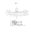
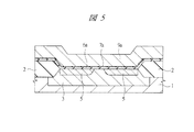
図1は、本実施の形態1におけるMISトランジスタQの断面図である。半導体基板1上には素子を分離するための素子分離領域2が形成されており、この素子分離領域2で分離された活性領域には、p型あるいはn型のウェル3が形成されている。このウェル3内には、不純物拡散領域5が形成される。
FIG. 1 is a cross-sectional view of the MIS transistor Q in the first embodiment. An
このウェル3上には、MISトランジスタQが形成されている。このMISトランジスタQを構成するゲート絶縁膜8は、第1絶縁物6および第2絶縁物7を有しており、この第2絶縁物7は、第1絶縁物6上に形成されている。
A MIS transistor Q is formed on the
この第1絶縁物6は、例えば、酸化シリコン(SiO2)膜であり、第2絶縁物7は、金属の酸化物からなる層であり、例えば、酸化タンタル(TaOx)層である。なお、本実施の形態1では、第1絶縁物6に、酸化シリコン膜を用いたが、窒化シリコン(SiN)膜、酸窒化シリコン(SiON)膜であっても良い。
The first insulator 6 is, for example, a silicon oxide (SiO 2 ) film, and the
また、第2絶縁物7は、ゲート電極材料の構成元素となる希土類金属の酸化物層であり、本実施の形態1では、タンタルの酸化物(TaOx)から形成されている。なお、第2絶縁物7の厚さは、MISトランジスタQを微細化する観点から、0.1nm〜2.0nm程度であることが望ましい。
The
このゲート絶縁膜8上には、ゲート電極9が形成されている。このゲート電極9は、金属を含む材料からなる導電体膜(金属膜)から形成され、本実施の形態1では、タンタル(Ta)を含む電極材料となる窒化タンタル(TaN)から形成されている。この窒化タンタルの仕事関数は、4.4eV程度であり、Siの伝導帯近傍(4.05eV近傍)と価電子帯近傍(5.17eV近傍)の間にあり、熱的安定性を備えているとともに、導電体膜としての密着性もよい。このため、TaN膜9が、ゲート絶縁膜8と反応したり、あるいは、剥離したり、さらには、金属原子(Ta)が、ゲート絶縁膜8、半導体基板1へ拡散して、MISトランジスタQの電気的特性が劣化することを防止することができる。
A
このように、本実施の形態1では、MISトランジスタQのゲート電極9の材料にTaN(窒化タンタル)を用いて、そのTaNを構成する金属であるTaと同一種類の金属(Ta)の酸化物層である酸化タンタル(TaOx)層(第2絶縁物7)と、酸化シリコン膜(第1絶縁物6)と、を含むゲート絶縁膜8を有するMISトランジスタQについて説明している。
As described above, in the first embodiment, TaN (tantalum nitride) is used as the material of the
ここで、本実施の形態1で示す、酸化シリコン膜(第1絶縁物)6と酸化タンタル層(第2絶縁物)7とからなるゲート絶縁膜8を有するMISトランジスタQと、酸化シリコン膜(第1絶縁物)のみからなるゲート絶縁膜を有するMISトランジスタとの電気特性を比較したところ、本実施の形態1で示すMISトランジスタQのフラットバンド電圧が、酸化シリコン膜のみからなるゲート絶縁膜を有するMISトランジスタのフラットバンド電圧に対して、0.3V程度正方向にシフトさせることができた。よって、金属の酸化物層(本実施の形態1では、酸化タンタル層)を含む、あるいは、含まないゲート絶縁膜からなるMIS構造を選択することで、MISトランジスタのしきい値電圧を制御することができるといえる。なお、フラットバンド電圧が正方向にシフトする理由として、酸化タンタル層7とゲート電極9との界面に形成される電気的ダイポールや酸化タンタル層7中に存在する負の固定電荷が影響しているものと考えることができる。
Here, the MIS transistor Q having the gate insulating film 8 composed of the silicon oxide film (first insulator) 6 and the tantalum oxide layer (second insulator) 7 shown in the first embodiment, and the silicon oxide film ( When comparing the electrical characteristics with the MIS transistor having the gate insulating film made only of the first insulator), the flat band voltage of the MIS transistor Q shown in the first embodiment shows that the gate insulating film made only of the silicon oxide film is It was possible to shift about 0.3 V in the positive direction with respect to the flat band voltage of the MIS transistor. Therefore, the threshold voltage of the MIS transistor is controlled by selecting a MIS structure including a gate insulating film that includes or does not include a metal oxide layer (the tantalum oxide layer in the first embodiment). Can be said. The reason why the flat band voltage shifts in the positive direction is influenced by an electric dipole formed at the interface between the
以上のことから、第1絶縁物(本実施の形態1では、酸化シリコン膜を示した)のみからなるゲート絶縁膜をn型MISトランジスタに、第1絶縁物(本実施の形態1では、酸化シリコン膜を示した)と第2絶縁物(本実施の形態1では、酸化タンタルを示した)とを含むゲート絶縁膜をp型MISトランジスタに適用することで、n型MISトランジスタとp型MISトランジスタとを備えた半導体装置を形成することができる。 From the above, the gate insulating film made only of the first insulator (the silicon oxide film is shown in the first embodiment) is changed to the n-type MIS transistor, and the first insulator (the oxide oxide in the first embodiment is oxidized). By applying a gate insulating film including a silicon film and a second insulator (in the first embodiment, tantalum oxide) to the p-type MIS transistor, the n-type MIS transistor and the p-type MIS transistor are applied. A semiconductor device including a transistor can be formed.
次に、MISトランジスタQの製造方法について、p型MISトランジスタに適用し、図面を参照しながら説明する。 Next, a method for manufacturing the MIS transistor Q will be described with reference to the drawings, which is applied to a p-type MIS transistor.
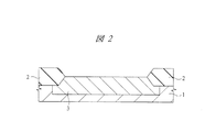
まず、図2に示すように、例えば、単結晶シリコンにボロン(B)などのp型不純物を導入した半導体基板1を用意する。次に、半導体基板1の主面上に素子分離領域2を形成する。素子分離領域2は、例えば、酸化シリコン膜よりなり、STI(Shallow Trench Isolation)法やLOCOS(Local Oxidization Of Silicon)法などによって形成される。図2では、窒化シリコン膜の耐酸化性を利用して半導体基板1の所定領域を選択酸化するLOCOS法によって形成された素子分離領域2を示している。
First, as shown in FIG. 2, for example, a
続いて、半導体基板1内にn型ウェル3を形成する。n型ウェル3は、例えば、イオン注入法を使用して、リンやヒ素などのn型不純物を半導体基板1内に導入することにより形成される。
Subsequently, an n-
続いて、図3に示すように、半導体基板1上に、例えば、CVD(Chemical Vapor Deposition)法を使用してポリシリコンやアモルファスシリコンのようなシリコン膜を形成した後、このシリコン膜に対して、露光・現像をすることによりパターニングし、半導体基板1上にダミー電極4を形成する。このときパターニングは、ダミー電極4を形成する領域にシリコン膜が残るようにする。なお、ダミー電極4を酸化シリコン膜から形成するようにしたが、これに限らず窒化シリコン膜、レジスト膜などから形成してもよい。
Subsequently, as shown in FIG. 3, after a silicon film such as polysilicon or amorphous silicon is formed on the
続いて、ダミー電極4に、自己整合で半導体領域であるp型不純物拡散領域5を形成する。p型不純物拡散領域5は、例えば、イオン注入法を使用してボロンなどのp型不純物を半導体基板1内に導入することにより形成することができる。
Subsequently, a p-type
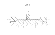
次に、図4に示すように、ダミー電極4を除去して、半導体基板1を洗浄した後、p型不純物拡散領域5に導入した不純物を活性化するための活性化アニールを行う。この活性化アニールは、例えば、850℃〜1050℃程度の高温で実施される。
Next, as shown in FIG. 4, after the dummy electrode 4 is removed and the
次に、図5に示すように、熱酸化法を使用して半導体基板1上に酸化シリコン膜6aを形成する。
Next, as shown in FIG. 5, a silicon oxide film 6a is formed on the
次に、酸化シリコン膜6a上に、原子層あるいは分子層レベルで堆積することができる方法、例えば、原子層制御成膜法(ALD: Atomic Layer Deposition法)を使用して、酸化タンタル層7aを5Å程度形成する。この酸化タンタル層7aの形成方法を以下に示す。
Next, the
まず、金属原料ガス、例えば、Ta(OC2H5)5を約300℃に加熱した半導体基板1に導入する。そして、窒素ガスにて排気した後、酸素反応ガスである水蒸気(H2O)を半導体基板1に導入し、窒素ガスで排気する。このようにして、約5Åの酸化タンタル層7aを形成する。なお、酸化タンタル層7aの形成に、ALD法を使用する例を示したが、これに限らず、間欠型CVD(Chemical Vapor Deposition)法などを使用して形成してもよい。
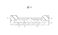
First, a metal source gas, for example, Ta (OC 2 H 5 ) 5 is introduced into the
続いて、酸素雰囲気中にて、この酸化タンタル層7aを高温、例えば、800℃程度でアニール処理する。なお、本実施の形態1では、酸素雰囲気中でアニール処理を行ったが、不活性雰囲気中で行ってもよい。また、本実施の形態1では、酸化タンタル層7aを800℃程度でアニール処理を行ったが、熱処理温度は、600℃〜900℃程度の範囲が好ましい。
Subsequently, the
次に、例えば、CVD法を使用して、400℃〜600℃程度に加熱された半導体基板1上に、窒化タンタル膜9aを形成する。なお、窒化タンタル膜9aの形成に、CVD法を使用する例を示したが、これに限らず、スパッタリング法、ALD法などを使用して形成してもよい。
Next, a
その後、図1に示したように、フォトリソグラフィ技術およびエッチング技術を使用して、酸化シリコン膜6および酸化タンタル層7からなるゲート絶縁膜8を形成し、このゲート絶縁膜8上に窒化タンタル膜9aよりなるゲート電極9を形成する。ここまでの工程によってn型ウェル3にp型MISトランジスタQを形成することができる。
Thereafter, as shown in FIG. 1, a gate insulating film 8 composed of a silicon oxide film 6 and a
また、本実施の形態1で示したMISトランジスタの製造方法では、ゲート電極9に高温の熱負荷が係らないため、以下に示すような効果が得られる。
Further, in the MIS transistor manufacturing method shown in the first embodiment, the
活性化アニール時のように高温の熱負荷が金属膜からなるゲート電極にかかると、ゲート電極とその下層に形成されているゲート絶縁膜が反応してしまい、反応により新たな絶縁物(酸化物)がゲート絶縁膜とゲート電極の間に形成される場合がある。この場合、ゲート電極の下層に形成されているゲート絶縁膜の膜厚が実質的に増加してしまい、駆動電流の低下やしきい値電圧の変動など、MISトランジスタの電気的特性が変動してしまうこととなる。しかし、本実施の形態1では、活性化アニールの後に金属膜よりなるゲート電極9を形成しているため、ゲート電極9には高温の熱負荷がかからず、ゲート電極9とゲート絶縁膜8との反応を防止することができる。したがって、本実施の形態1によれば、p型MISトランジスタQの電気的特性の変動を抑制することができる。
When a high-temperature heat load is applied to the gate electrode made of a metal film as in the activation annealing, the gate electrode and the gate insulating film formed below it react with each other, resulting in a new insulator (oxide) ) May be formed between the gate insulating film and the gate electrode. In this case, the film thickness of the gate insulating film formed under the gate electrode substantially increases, and the electrical characteristics of the MIS transistor fluctuate, such as a decrease in driving current and a variation in threshold voltage. It will end up. However, in the first embodiment, since the
また、ゲート電極に高温の熱負荷をかけると、ゲート電極に生ずる応力が増加するとともに界面における界面準位が増加する傾向が考えられる。しかし、本実施の形態1では、ゲート電極9の形成後に活性化アニールのような高温の熱処理を加えないため、応力の増加を抑制でき、応力や界面準位に起因したしきい値の変動およびキャリアの移動度の低下を抑制することができる。
In addition, when a high temperature heat load is applied to the gate electrode, the stress generated in the gate electrode increases and the interface state at the interface tends to increase. However, in the first embodiment, since a high-temperature heat treatment such as activation annealing is not performed after the
また、ゲート電極に高温の熱負荷をかけると、ゲート電極を構成する金属元素がゲート電極からゲート絶縁膜中や半導体基板内に拡散する場合がある。この場合、ゲート絶縁膜中に金属元素が拡散するとゲート絶縁膜の絶縁耐性が低下するとともにリーク電流が増加すると考えられる。一方、ゲート絶縁膜を突き抜けて半導体基板内に金属元素が拡散すると、しきい値電圧の変動を引き起こすことになる。しかし、本実施の形態1ではゲート電極9の形成後に活性化アニールのような高温の熱処理を加えないため、ゲート電極9を形成する金属元素がゲート絶縁膜8や半導体基板1内へ拡散することを抑制することができる。
In addition, when a high-temperature heat load is applied to the gate electrode, a metal element constituting the gate electrode may diffuse from the gate electrode into the gate insulating film or the semiconductor substrate. In this case, it is considered that when a metal element diffuses into the gate insulating film, the insulation resistance of the gate insulating film is lowered and the leakage current is increased. On the other hand, if a metal element diffuses into the semiconductor substrate through the gate insulating film, the threshold voltage fluctuates. However, since the high temperature heat treatment such as activation annealing is not applied after the formation of the
また、ゲート絶縁膜上にゲート電極を形成し、ゲート電極に高温の熱負荷がかかると、MISトランジスタのしきい値がシフトする場合がある。この場合、熱負荷により、ゲート絶縁膜とゲート電極の界面に酸化物の層ができて、MISトランジスタのしきい値をシフトさせるものと考えられる。しかし、本実施の形態1ではゲート電極9の形成後に活性化アニールのような高温の熱処理を加えないため、しきい値をシフトさせることなく、安定したしきい値設定をすることができる。
Further, when a gate electrode is formed on the gate insulating film and a high temperature heat load is applied to the gate electrode, the threshold value of the MIS transistor may shift. In this case, it is considered that an oxide layer is formed at the interface between the gate insulating film and the gate electrode due to the thermal load, and the threshold value of the MIS transistor is shifted. However, since the high temperature heat treatment such as activation annealing is not applied after the formation of the
また、本実施の形態1では、ゲート電極9にタンタルを構成元素とする窒化タンタルを適用し、ゲート絶縁膜8にタンタルの酸化物である酸化タンタル層を含む構造とするMISトランジスタQを示し、このMISトランジスタQのフラットバンド電圧が、酸化タンタル層を含まない構造のMISトランジスタのそれに対し、正方向にシフトすることを例示した。一方、例えば、ゲート電極材料を構成する金属に、ニッケル(Ni)、コバルト(Co)を用いて、MISトランジスタQのゲート絶縁膜8に含まれる金属の酸化物層7に、酸化ニッケル(NiO)、酸化コバルト(CoO)を用いた場合には、これら金属の酸化物層を含まない構造のMISトランジスタのフラットバンド電圧に対し、負方向にシフトさせることができる。
Further, in the first embodiment, a MIS transistor Q having a structure in which tantalum nitride containing tantalum as a constituent element is applied to the
(実施の形態2)
本発明の実施の形態2では、ゲート電極材料の構成元素となる金属と、同一の金属の酸化物層を有するゲート絶縁膜を備えたMISトランジスタ、および、その製造技術について、図6〜図14を用いて説明する。
(Embodiment 2)
In
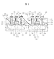
図6は、本実施の形態2におけるn型MISトランジスタQ1およびp型MISトランジスタQ2を備えた半導体装置の断面図である。図6において、半導体基板101上には素子を分離するための素子分離領域102が形成されており、この素子分離領域102で分離された活性領域にはp型ウェル103とn型ウェル104とが形成されている。
FIG. 6 is a cross-sectional view of a semiconductor device including the n-type MIS transistor Q 1 and the p-type MIS transistor Q 2 in the second embodiment. In FIG. 6, an
p型ウェル103上にはn型MISトランジスタQ1が形成されており、n型ウェル104上にはp型MISトランジスタQ2が形成されている。
An n-type MIS transistor Q 1 is formed on the p-
このn型MISトランジスタQ1は、例えば、酸化シリコン膜111よりなるゲート絶縁膜114を有しており、このゲート絶縁膜114上にゲート電極115を有している。このゲート電極115は、例えば、窒化タンタル(TaN)膜から構成されている。この窒化タンタルの仕事関数は、4.4eV程度であり、シリコンの伝導帯近傍(4.05eV近傍)と価電子帯近傍(5.17eV近傍)の間にあり、熱的安定性を備えているとともに膜の密着性もよい。なお、ゲート電極材料の例として、TaNを使用する例を示したが、これに限らず、Ta、TiN、Ti、HfN、Hf、ZrN、Zr、Alおよび希土類金属およびこれら金属材料中にSiを有する材料を使用することができる。
The n-type MIS transistor Q 1 has a
また、ゲート電極115の側壁には、絶縁膜よりなるサイドウォール118が形成されており、サイドウォール118下のp型ウェル103内には半導体領域である低濃度n型不純物拡散領域106が形成されている。この低濃度n型不純物拡散領域106の外側には低濃度n型不純物拡散領域106より不純物密度が高い高濃度n型不純物拡散領域109が形成されている。低濃度n型不純物拡散領域106および高濃度n型不純物拡散領域109によりn型MISトランジスタQ1のソース領域およびドレイン領域が形成される。
A
また、p型MISトランジスタQ2は、例えば、酸化シリコン膜111および金属の酸化物層(酸化金属物層)112からなるゲート絶縁膜116を有しており、このゲート絶縁膜116上にゲート電極115を有している。このゲート電極115は、n型MISトランジスタQ1と同一のゲート電極材料からなり、本実施の形態1では、窒化タンタル(TaN)膜から構成されている。また、酸化金属物層112は、ゲート電極材料の構成元素となる金属の酸化物層であり、本実施の形態1では、Taの酸化物層(酸化タンタル層)である。なお、酸化金属物層112の厚さは、MISトランジスタを微細化する観点から、例えば、0.1nm〜2.0nm程度であることが望ましい。
The p-type MIS transistor Q 2 has a
また、p型MISトランジスタQ2のゲート電極115の側壁には、絶縁膜よりなるサイドウォール118が形成されており、サイドウォール118下のn型ウェル104内には半導体領域である低濃度p型不純物拡散領域107が形成されている。この低濃度p型不純物拡散領域107の外側には低濃度p型不純物拡散領域107より不純物密度が高い高濃度p型不純物拡散領域110が形成されている。低濃度p型不純物拡散領域107および高濃度p型不純物拡散領域110によりp型MISトランジスタQ2のソース領域およびドレイン領域が形成される。
Further, a
また、半導体基板101に形成されたn型MISトランジスタQ1およびp型MISトランジスタQ2上には、層間絶縁膜119が形成されており、この層間絶縁膜119には、n型MISトランジスタQ1、および、p型MISトランジスタQ2のソース領域、ドレイン領域に貫通するコンタクトホール120が形成されている。
Further, on the n-type MIS transistor Q 1 and the p-type MIS transistor Q 2 is formed on the
このコンタクトホール120の内壁には、チタン/窒化チタン膜121aが形成されており、このチタン/窒化チタン膜121aを介してコンタクトホール120にはタングステン膜121bが埋め込まれ、プラグ121が形成されている。チタン/窒化チタン膜121aは、例えば、タングステンの拡散を抑制する機能および下地との密着性を向上させる機能を有している。
A titanium /
また、層間絶縁膜119上には、チタン/窒化チタン膜122a、アルミニウム膜122b、チタン/窒化チタン膜122cよりなるパターニングされた配線122が形成されている。なお、図示はしないが、配線上には、層間絶縁膜を貫通するプラグを介して多層配線が形成されている。
On the
以上述べたように、本実施の形態2で示す、n型MISトランジスタQ1とp型MISトランジスタQ2とを備えた半導体装置において、酸化シリコン膜111のみからなるゲート絶縁膜114をn型MISトランジスタに、酸化シリコン膜111と酸化タンタル層112とを含むゲート絶縁膜116をp型MISトランジスタに、適用することができる。
As described above, in the semiconductor device including the n-type MIS transistor Q 1 and the p-type MIS transistor Q 2 shown in the second embodiment, the
また、本実施の形態2では、ゲート電極材料膜に対してイオン注入を行っていない。すなわち、n型およびp型用のゲート電極材料膜を形成し、その後、一方のMISトランジスタのゲート電極材料膜にイオン注入することで、n型とp型とのゲート電極の仕事関数とを異ならせるようなシングルメタルゲートで問題となる、イオン注入によるゲート絶縁膜等へのダメージの影響を受けることなく、MISトランジスタのゲート絶縁膜を形成することができる。 In the second embodiment, ion implantation is not performed on the gate electrode material film. That is, n-type and p-type gate electrode material films are formed, and then ion implantation is performed on the gate electrode material film of one of the MIS transistors, so that the work functions of the n-type and p-type gate electrodes are different. The gate insulating film of the MIS transistor can be formed without being affected by damage to the gate insulating film or the like caused by ion implantation, which is a problem with such a single metal gate.
また、本実施の形態2で示したn型MISトランジスタとp型MISトランジスタとを備えた半導体装置は、別の種類の電極材料をそれぞれn型およびp型のゲート電極材料として、あるいは、同一種類の電極材料を処理してn型およびp型のゲート電極材料として、用いていない。しかし、同一種類の材料をn型およびp型のゲート電極材料とし、p型あるいはn型のゲート絶縁膜のゲート電極との界面に、金属の酸化物層を含むことで、例えば、CMOSトランジスタを提供することができる。 In the semiconductor device including the n-type MIS transistor and the p-type MIS transistor shown in the second embodiment, different types of electrode materials are used as n-type and p-type gate electrode materials, respectively, or the same type. Are not used as n-type and p-type gate electrode materials. However, by using the same type of material as the n-type and p-type gate electrode materials and including a metal oxide layer at the interface with the gate electrode of the p-type or n-type gate insulating film, for example, a CMOS transistor Can be provided.
また、本実施の形態2で示す、5Å程度の厚さの酸化タンタル層112は、高誘電率の誘電体層でもあるため、酸化シリコン膜111と酸化タンタル層112とからなるゲート絶縁膜116の酸化シリコン換算膜厚(EOT:Equivalent Oxide Thickness)の増加を抑えることができる。
In addition, since the
次に、上記のn型MISトランジスタとp型MISトランジスタとを備えた半導体装置の製造方法について、図面を参照しながら説明する。 Next, a method for manufacturing a semiconductor device including the n-type MIS transistor and the p-type MIS transistor will be described with reference to the drawings.
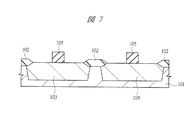
まず、図7に示すように、例えば、単結晶シリコンにボロン(B)などのp型不純物を導入した半導体基板101を用意する。次に、半導体基板101の主面上に素子分離領域102を形成する。素子分離領域102は、例えば、酸化シリコンからなり、STI(Shallow Trench Isolation)法やLOCOS(Local Oxidization Of Silicon)法などによって形成される。図7では、窒化シリコン膜の耐酸化性を利用して半導体基板101の所定領域を選択酸化するLOCOS法によって形成された素子分離領域102を示している。
First, as shown in FIG. 7, for example, a
続いて、半導体基板101内にp型ウェル103を形成する。p型ウェル103は、例えば、フォトリソグラフィ技術およびイオン注入法を利用して、ボロンやフッ化ボロンなどのp型不純物を半導体基板101内に導入することにより形成される。同様に、半導体基板101内にn型ウェル104を形成する。n型ウェル104は、例えば、フォトリソグラフィ技術およびイオン注入法を使用して、リンやヒ素などのn型不純物を半導体基板101内に導入することにより形成される。
Subsequently, a p-
次に、半導体基板101の主面上に、例えば、CVD法を使用してポリシリコンやアモルファスシリコンのようなシリコン膜を形成した後、このシリコン膜に対して、露光・現像をすることによりパターニングし、半導体基板101上にダミー電極105を形成する。このときパターニングは、ダミー電極105を形成する領域にシリコン膜が残るようにする。なお、ダミー電極105をシリコン膜から形成するようにしたが、これに限らず窒化シリコン膜などから形成してもよい。
Next, after a silicon film such as polysilicon or amorphous silicon is formed on the main surface of the
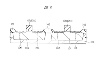
次に、図8に示すように、半導体基板101内であって、ダミー電極105aに整合して、半導体領域である低濃度n型不純物拡散領域106を形成する。低濃度n型不純物拡散領域106は、例えば、フォトリソグラフィ技術およびイオン注入法を使用して、リンやヒ素などのn型不純物を半導体基板101内に導入することにより形成することができる。同様に、ダミー電極105bに整合して、半導体領域である低濃度p型不純物拡散領域107を形成する。低濃度p型不純物拡散領域107は、例えば、フォトリソグラフィ技術およびイオン注入法を使用してボロンなどのp型不純物を半導体基板101内に導入することにより形成することができる。
Next, as shown in FIG. 8, in the
続いて、図9に示すように、半導体基板101の主面上に、例えば、プラズマCVD法を使用して窒化シリコン膜を形成した後、この窒化シリコン膜に対して異方性エッチングすることにより、ダミー電極105の側壁にサイドウォール108を形成する。なお、サイドウォール108を窒化シリコン膜より形成したが、これに限らず、例えば、酸化シリコン膜、酸窒化シリコン膜あるいは酸化シリコン膜と窒化シリコン膜との積層膜から形成しても良い。
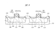
Subsequently, as shown in FIG. 9, a silicon nitride film is formed on the main surface of the
次に、サイドウォール108aに整合して、半導体基板101内の領域内に高濃度n型不純物拡散領域109を形成する。高濃度n型不純物拡散領域109は、例えば、フォトリソグラフィ技術およびイオン注入法を使用して形成され、低濃度n型不純物拡散領域106よりも高濃度にしてリンやヒ素などのn型不純物が導入されている。同様に、サイドウォール108bに整合して、半導体基板101内の領域に高濃度p型不純物拡散領域110を形成する。高濃度p型不純物拡散領域110は、例えば、フォトリソグラフィ技術およびイオン注入法を使用して形成され、低濃度p型不純物拡散領域107よりも高濃度にしてボロンなどのp型不純物が導入されている。
Next, a high concentration n-type
次に、ダミー電極105、サイドウォール108は除去され、半導体基板101を洗浄した後、低濃度n型不純物拡散領域106、低濃度p型不純物拡散領域107、高濃度n型不純物拡散領域109および高濃度p型不純物拡散領域110に導入した不純物を活性化するたの活性化アニールを行う。この活性化アニールは、例えば、850℃〜1050℃程度の高温で実施される。
Next, the
上述した、ダミー電極105を形成し、このダミー電極105に整合してMISトランジスタの低濃度n型不純物拡散領域106、低濃度p型不純物拡散領域107、高濃度n型不純物拡散領域109および高濃度p型不純物拡散領域110を形成した後、それら不純物拡散領域内の不純物を活性化するための活性化アニールを行う工程では、一般的なMISトランジスタの製造方法のように、ゲート電極を形成した後に不純物の活性化アニールを行っていない。このため、一般的な半導体装置の製造方法では、活性化アニールによりゲート電極に高温の熱負荷がかかるが、本実施の形態2における半導体装置の製造方法では、後の工程で形成されるゲート電極に、高温の熱負荷をかけずに済むことができる。
The above-described
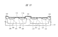
続いて、図10に示すように、熱酸化法を使用して、半導体基板101上に酸化シリコン膜111を形成する。
Subsequently, as shown in FIG. 10, a
次に、酸化シリコン膜111上に、例えば、原子層制御成膜法(ALD: Atomic Layer Deposition法)を使用して、酸化金属物層である酸化タンタル(TaOx)層112aを5Å程度形成する。具体的には、タンタル(Ta)の原料ガス、例えば、Ta(OC2H5)5を約300℃に加熱した半導体基板101上に導入する。そして、窒素ガスにてTaの原料ガスを排気した後、水蒸気(H2O)を半導体基板101に導入し、窒素ガスで排気する。このようにして、5Å程度の酸化タンタル層112aを形成する。なお、酸化タンタル層112aの形成に、ALD法を使用する例を示したが、これに限らず、間欠型CVD(Chemical Vapor Deposition)法などを使用して形成してもよい。
Next, a tantalum oxide (TaOx)
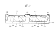
次に、図11に示すように、フォトリソグラフィ技術およびエッチング技術を使用して、酸化タンタル層112aをエッチングし、p型MISトランジスタ形成領域に酸化タンタル層112を形成する。
Next, as shown in FIG. 11, the
次に、酸素雰囲気中にて、この酸化タンタル層112を高温、例えば、800℃程度でアニール処理する。なお、本実施の形態2では、酸素雰囲気中でアニール処理を行ったが、不活性雰囲気中で行ってもよい。また、本実施の形態2では、酸化タンタル層112を800℃程度でアニール処理を行ったが、熱処理温度は、600℃〜900℃程度の範囲が好ましい。
Next, the
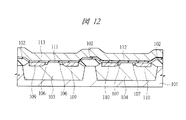
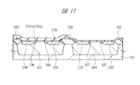
次に、図12に示すように、例えば、CVD法を使用して、400℃〜600℃程度に加熱された半導体基板101上に、窒化タンタル膜113を形成する。なお、窒化タンタル膜113の形成に、CVD法を使用する例を示したが、これに限らず、スパッタリング法、ALD法などを使用して形成してもよい。
Next, as shown in FIG. 12, a
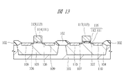
次に、図13に示すように、フォトリソグラフィ技術およびエッチング技術を使用して、n型MISトランジスタ形成領域に、窒化タンタル113よりなるゲート電極115を形成し、このゲート電極115下に酸化シリコン膜111よりなるゲート絶縁膜114を形成する。また、p型MISトランジスタ形成領域に、窒化タンタル113よりなるゲート電極117を形成し、このゲート電極117下に酸化タンタル層112および酸化シリコン膜111からなるゲート絶縁膜116を形成する。
Next, as shown in FIG. 13, a
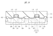
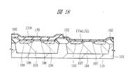
次に、図14に示すように、半導体基板101の主面上に、例えば、プラズマCVD法などを使用して半導体基板101上に窒化シリコン膜を形成した後、この窒化シリコン膜に対して異方性エッチングを行うことにより、サイドウォール118を形成する。
Next, as shown in FIG. 14, after a silicon nitride film is formed on the main surface of the
次に、CVD法を使用して、半導体基板101の主面上に酸化シリコン膜よりなる層間絶縁膜119を形成した後、CMP法を使用して、表面を平坦化する。
Next, an
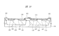
次に、図6に示すように、フォトリソグラフィ技術およびエッチング技術を使用して、層間絶縁膜119にコンタクトホール120を形成する。次いで、コンタクトホール120の底面、内壁および層間絶縁膜119上にチタン/窒化チタン膜121aを形成する。このチタン/窒化チタン膜121aは、チタン膜と窒化チタン膜の積層膜から形成され、例えば、スパッタリング法を使用することにより形成できる。
Next, as shown in FIG. 6, a
次に、コンタクトホール120を埋め込むように、タングステン膜121bを形成する。タングステン膜121bは、例えば、CVD法を使用することにより形成することができる。そして、半導体基板101上に堆積された不要なチタン/窒化チタン膜121aおよびタングステン膜121bを、例えば、CMP法を使用して除去することにより、プラグ121を形成する。
Next, a
次に、層間絶縁膜119およびプラグ121上にチタン/窒化チタン膜122a、アルミニウム膜122b、チタン/窒化チタン膜122cを順次、形成する。これらの膜は、例えば、スパッタリング法を使用することにより形成できる。次いで、フォトリソグラフィ技術およびエッチング技術を使用することにより、これらの膜のパターニングを行い、配線122が形成される。
Next, a titanium /
このようにして、nチャネル型MISトランジスタQ1およびpチャネル型MISトランジスタQ2を形成することができる。なお、配線122の形成後、上述した層間絶縁膜119、プラグ121、配線122を形成する工程と同様の工程を繰り返すことにより、配線122の上部に多層に配線を形成し、最後にパッシベーション膜で半導体基板101の全体を覆うことにより、CMOSデバイスが完成する。
In this way, the n-channel MIS transistor Q 1 and the p-channel MIS transistor Q 2 can be formed. Note that after the
本実施の形態2で示したnチャネル型MISトランジスタQ1およびにpチャネル型MISトランジスタQ2で異なるゲート絶縁膜構造を有する半導体装置とすることで、しきい値制御が可能となり、その結果消費電力の低い半導体装置を製造することができる。 By using the semiconductor device having different gate insulating film structures for the n-channel type MIS transistor Q 1 and the p-channel type MIS transistor Q 2 shown in the second embodiment, threshold value control becomes possible, resulting in consumption. A semiconductor device with low power can be manufactured.
また、本実施の形態2で示したnチャネル型MISトランジスタQ1およびにpチャネル型MISトランジスタQ2を有する半導体装置は、一般的に適用されるデュアルメタルゲート構造ではない。すなわち、本実施の形態2で示したnチャネル型MISトランジスタQ1およびpチャネル型MISトランジスタQ2を有する半導体装置の製造方法は、p型(あるいはn型)のゲート電極材料膜を形成し、次いで、n型(あるいはp型)のMISトランジスタが形成される領域内のゲート電極材料膜を選択的に除去し、その後、n型(あるいはp型)のゲート電極材料膜を形成する工程を含まない。このため、ゲート電極材料を除去する際のエッチング液やレジストを剥離する際の剥離液にゲート絶縁膜が晒されず、本実施の形態2における半導体装置の製造方法を適用することで、ゲート絶縁膜等の信頼性が大幅に向上することができる。 Further, the semiconductor device having the n-channel MIS transistor Q 1 and the p-channel MIS transistor Q 2 shown in the second embodiment does not have a dual metal gate structure that is generally applied. That is, the method of manufacturing a semiconductor device having the n-channel MIS transistor Q 1 and the p-channel MIS transistor Q 2 shown in the second embodiment forms a p-type (or n-type) gate electrode material film, Next, the method includes selectively removing a gate electrode material film in a region where an n-type (or p-type) MIS transistor is to be formed, and then forming an n-type (or p-type) gate electrode material film. Absent. For this reason, the gate insulating film is not exposed to the etching solution for removing the gate electrode material or the stripping solution for stripping the resist, and the gate insulating film can be obtained by applying the semiconductor device manufacturing method according to the second embodiment. The reliability of the film or the like can be greatly improved.
(実施の形態3)
前記実施の形態2では、ゲート絶縁膜を構成する、金属の酸化物層を、原子層制御成膜法(ALD: Atomic Layer Deposition法)を使用して形成する例について説明したが、本実施の形態3では、金属膜を熱酸化することにより、金属の酸化物層を形成する例について説明する。
(Embodiment 3)
In the second embodiment, the example in which the metal oxide layer constituting the gate insulating film is formed by using an atomic layer control film formation method (ALD: Atomic Layer Deposition method) has been described. In
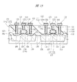
図15は、本実施の形態3におけるn型MISトランジスタQ3およびp型MISトランジスタQ4を示した断面図である。図15において、n型MISトランジスタQ3およびp型MISトランジスタのそれぞれの構成は、前記実施の形態2のn型MISトランジスタQ1およびp型MISトランジスタQ2の構成とほぼ同様であるが、n型MISトランジスタQ3およびp型MISトランジスタQ4を製造する方法において相違点があるため、以下説明する。 FIG. 15 is a cross-sectional view showing n-type MIS transistor Q 3 and p-type MIS transistor Q 4 in the third embodiment. In FIG. 15, the configurations of the n-type MIS transistor Q 3 and the p-type MIS transistor are substantially the same as the configurations of the n-type MIS transistor Q 1 and the p-type MIS transistor Q 2 of the second embodiment. Since there is a difference in the method of manufacturing the type MIS transistor Q 3 and the p-type MIS transistor Q 4 , a description will be given below.
まず、前記実施の形態2で示した図7〜図9で示した工程までは同様である。 First, the process is the same up to the steps shown in FIGS. 7 to 9 shown in the second embodiment.
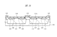
次に、図16に示すように、熱酸化法を使用して、半導体基板101上に酸化シリコン膜130を形成する。
Next, as shown in FIG. 16, a
続いて、酸化シリコン膜130上に、例えば、プラズマCVD法を使用して窒化シリコン膜131aを形成する。
Subsequently, a
次に、図17に示すように、フォトリソグラフィ技術およびエッチング技術を使用して、p型MISトランジスタQ4領域の半導体基板101上の窒化シリコン膜131aを除去し、n型MISトランジスタQ3領域の半導体基板101上には窒化シリコン膜131a(131b)を残す。
Next, as shown in FIG. 17, using photolithography and etching to remove the p-type MIS transistor Q 4 silicon nitride on the
次に、図18に示すように、この半導体基板101上に、n型MISトランジスタQ3およびp型MISトランジスタQ4のゲート電極材料(本実施の形態3では、TaNを示す)と同一種類の金属(本実施の形態3では、Taを示す)の金属物層132を、例えば、CVD法を使用して堆積する。
Next, as shown in FIG. 18, on the
次に、この金属物層132に熱酸化処理を800℃程度で行うことにより、金属の酸化物層(本実施の形態3では、酸化タンタル層を示す)133aが形成される。なお、本実施の形態3では、酸素雰囲気中に置かれた半導体基板101を800℃程度の熱処理で行ったが、熱処理温度は、600℃〜1000℃程度の範囲が好ましい。
Next, thermal oxidation treatment is performed on the
次に、図19に示すように、フォトリソグラフィ技術およびエッチング技術を使用して、酸化タンタル層133aをエッチングし、p型MISトランジスタ領域に酸化金属物層133を形成する。
Next, as shown in FIG. 19, the
この後の工程は、前記実施の形態2で図12〜図14および図6を用いて説明した工程と同様であり、それらの工程後、図15に示すように、n型MISトランジスタQ3およびp型MISトランジスタQ4を形成することができる。なお、配線122の形成後、層間絶縁膜119、プラグ121、配線122を形成する工程と同様の工程を繰り返すことにより、配線122の上部に多層に配線を形成し、最後にパッシベーション膜で半導体基板101の全体を覆うことにより、CMOSデバイスが完成する。
The subsequent steps are the same as those described with reference to FIGS. 12 to 14 and FIG. 6 in the second embodiment. After these steps, as shown in FIG. 15, the n-type MIS transistor Q 3 and A p-type MIS transistor Q 4 can be formed. Note that, after the
本実施の形態3で示したnチャネル型MISトランジスタQ3のゲート絶縁膜134とp型MISトランジスタQ4のゲート絶縁膜135とを異なる構造とする半導体装置は、前記実施の形態2で示した半導体装置の効果と、同様の効果を得ることができる。
The semiconductor device in which the
また、酸化金属物層133を形成する工程は、ゲート電極材料(本実施の形態3では、TaN)と同一種類の金属(本実施の形態3では、Ta)の金属膜を、p型MISトランジスタQ4領域の酸化シリコン膜上に堆積させた後、熱酸化処理するため、酸化金属物層を形成する装置およびその工程が省略することができる。
In addition, the step of forming the
以上、本発明者によってなされた発明を実施の形態に基づき具体的に説明したが、本発明は前記実施の形態に限定されるものではなく、その要旨を逸脱しない範囲で種々変更可能であることはいうまでもない。 As mentioned above, the invention made by the present inventor has been specifically described based on the embodiment. However, the present invention is not limited to the embodiment, and various modifications can be made without departing from the scope of the invention. Needless to say.
例えば、前記実施の形態1〜3では、ゲート電極材料は、TaN(窒化タンタル)を用いたが、Ta、Ti、TiN、Hf、HfN、Zr、ZrN、Alおよび希土類金属、あるいは、これら金属材料中にSiを有する材料であってもよい。
For example, in
また、前記実施の形態2および前記実施の形態3では、n型MISトランジスタとp型MISトランジスタのゲート電極材料に同一種類の材料を使用し、p型MISトランジスタのゲート絶縁膜には、その金属材料の酸化物層を含み、n型MISトランジスタのゲート絶縁膜では、酸化物層を含まない構造としたが、p型MISトランジスタのゲート絶縁膜には、金属の酸化物層を含まず、n型MISトランジスタのゲート絶縁膜に、金属の酸化物層を含む構造としてもよい。例えば、ゲート電極材料を構成する金属に、ニッケル(Ni)、コバルト(Co)を用いて、p型MISトランジスタのゲート絶縁膜に含まれる金属の酸化物層に、酸化ニッケル(NiO)、酸化コバルト(CoO)を用いた場合である。 In the second and third embodiments, the same type of material is used for the gate electrode material of the n-type MIS transistor and the p-type MIS transistor, and the metal film is used for the gate insulating film of the p-type MIS transistor. The gate insulating film of the n-type MIS transistor includes the oxide layer of the material and does not include the oxide layer. However, the gate insulating film of the p-type MIS transistor does not include the metal oxide layer. The gate insulating film of the type MIS transistor may include a metal oxide layer. For example, nickel (Ni) or cobalt (Co) is used as the metal constituting the gate electrode material, and nickel oxide (NiO) or cobalt oxide is used as the metal oxide layer included in the gate insulating film of the p-type MIS transistor. This is a case where (CoO) is used.
また、前記実施の形態1〜3では、酸化シリコン(第1絶縁膜)および酸化金属物層(第2絶縁膜)を含むゲート絶縁膜を使用したが、これに限らず、第1絶縁膜には、例えば、酸窒化シリコン(SiON)膜、また、第2絶縁膜には、例えば、Hf、Zr、Ta、Al、Ti、Nb、Sc、Y、La、Ce、Pr、Nd、Sm、Eu、Gd、Tb、Dy、Ho、Er、Tm、YbおよびLuからなる群から選ばれる少なくとも一種を含む金属シリケート層としてもよい。 In the first to third embodiments, the gate insulating film including the silicon oxide (first insulating film) and the metal oxide layer (second insulating film) is used. For example, a silicon oxynitride (SiON) film and a second insulating film include, for example, Hf, Zr, Ta, Al, Ti, Nb, Sc, Y, La, Ce, Pr, Nd, Sm, Eu , Gd, Tb, Dy, Ho, Er, Tm, Yb, and a metal silicate layer containing at least one selected from the group consisting of Lu and Lu.
本発明は、半導体装置を製造する製造業に幅広く利用されるものである。 The present invention is widely used in the manufacturing industry for manufacturing semiconductor devices.
1 半導体基板
2 素子分離領域
3 ウェル(n型ウェル)
4 ダミー電極
5 不純物拡散領域
6、6a 酸化シリコン膜
7、7a 酸化タンタル層
8 ゲート絶縁膜
9 ゲート電極
9a 窒化タンタル膜
101 半導体基板
102 素子分離領域
103 p型ウェル
104 n型ウェル
105、105a、105b ダミー電極
106 低濃度n型不純物拡散領域
107 低濃度p型不純物拡散領域
108、108a、108b サイドウォール
109 高濃度n型不純物拡散領域
110 高濃度p型不純物拡散領域
111 酸化シリコン膜
112、112a 酸化金属物層(酸化タンタル層)
113 窒化タンタル膜
114 ゲート絶縁膜(n型MISトランジスタのゲート絶縁膜)
115 ゲート電極(n型MISトランジスタのゲート電極)
116 ゲート絶縁膜(p型MISトランジスタのゲート絶縁膜)
117 ゲート電極(p型MISトランジスタのゲート電極)
118 サイドウォール
119 層間絶縁膜
120 コンタクトホール
121a チタン/窒化チタン膜
121b タングステン膜
121 プラグ
122a チタン/窒化チタン膜
122b アルミニウム膜
122c チタン/窒化チタン膜
122 配線
130 酸化シリコン膜
131、131a、131b 窒化シリコン膜
132 金属物層
133、133a 酸化金属物層(酸化タンタル層)
134 ゲート絶縁膜(n型MISトランジスタのゲート絶縁膜)
135 ゲート絶縁膜(p型MISトランジスタのゲート絶縁膜)
Q MISトランジスタ(p型MISトランジスタ)
Q1 n型MISトランジスタ
Q2 p型MISトランジスタ
Q3 n型MISトランジスタ
Q4 p型MISトランジスタ
DESCRIPTION OF
4
113
115 Gate electrode (gate electrode of n-type MIS transistor)
116 Gate insulating film (gate insulating film of p-type MIS transistor)
117 Gate electrode (gate electrode of p-type MIS transistor)
118
134 Gate insulating film (gate insulating film of n-type MIS transistor)
135 Gate insulating film (p-type MIS transistor gate insulating film)
Q MIS transistor (p-type MIS transistor)
Q 1 n-type MIS transistor Q 2 p-type MIS transistor Q 3 n-type MIS transistor Q 4 p-type MIS transistor
Claims (5)
前記MISトランジスタのゲート絶縁膜は、前記ゲート電極との界面に、前記金属の酸化物からなる層を有することを特徴とする半導体装置。 A semiconductor device including a MIS transistor having a gate electrode formed of a conductor film made of a material containing a metal,
The semiconductor device according to claim 1, wherein the gate insulating film of the MIS transistor has a layer made of the metal oxide at an interface with the gate electrode.
前記第1ゲート電極および前記第2ゲート電極は、金属を含む材料からなる同一の導電体膜で形成され、
前記第1ゲート絶縁膜は、前記第1ゲート電極との界面に、前記金属の酸化物からなる層を有することを特徴とする半導体装置。 A semiconductor device comprising: a first MIS transistor including a first gate electrode and a first gate insulating film; and a second MIS transistor including a second gate electrode and a second gate insulating film,
The first gate electrode and the second gate electrode are formed of the same conductor film made of a material containing metal,
The semiconductor device according to claim 1, wherein the first gate insulating film has a layer made of the metal oxide at an interface with the first gate electrode.
前記金属の酸化物からなる層の厚さは、0.1nm以上、2.0nm以下であることを特徴とする半導体装置。 The semiconductor device according to claim 2,
The thickness of the layer made of the metal oxide is 0.1 nm or more and 2.0 nm or less.
(a)半導体基板の主面上にダミー電極を形成する工程と、
(b)前記ダミー電極に自己整合で、前記半導体基板内の領域に不純物拡散領域を形成する工程と、
(c)前記ダミー電極を除去する工程と、
(d)前記不純物拡散領域を活性化する工程と、
(e)前記半導体基板の主面上に前記第1絶縁物を形成する工程と、
(f)前記第1絶縁物上に、前記第2絶縁物となる、前記金属の酸化物からなる層を形成する工程と、
(g)前記第2絶縁物を高温で熱処理する工程と、
(h)前記第2絶縁物上に、前記ゲート電極を形成する工程と、
を有することを特徴とする半導体装置の製造方法。 A method of manufacturing a semiconductor device including a MIS transistor having a gate electrode formed of a conductor film made of a material including a metal, and a gate insulating film including a first insulator and a second insulator,
(A) forming a dummy electrode on the main surface of the semiconductor substrate;
(B) forming an impurity diffusion region in a region in the semiconductor substrate in a self-aligned manner with the dummy electrode;
(C) removing the dummy electrode;
(D) activating the impurity diffusion region;
(E) forming the first insulator on a main surface of the semiconductor substrate;
(F) forming a layer made of an oxide of the metal to be the second insulator on the first insulator;
(G) heat-treating the second insulator at a high temperature;
(H) forming the gate electrode on the second insulator;
A method for manufacturing a semiconductor device, comprising:
第2ゲート電極と、前記第1絶縁物を含む第2ゲート絶縁膜と、を有する第2MISトランジスタと、
を備える半導体装置の製造方法であって、
(a)半導体基板の主面上に前記第1MISトランジスタの第1ダミー電極、および、第2MISトランジスタの第2ダミー電極を形成する工程と、
(b)前記第1ダミー電極に自己整合で、前記半導体基板内の第1領域に第1不純物拡散領域を形成する工程と、
(c)前記第2ダミー電極に整合して、前記半導体基板内の第2領域に第2不純物拡散領域を形成する工程と、
(d)前記第1ダミー電極および前記第2ダミー電極を除去する工程と、
(e)前記第1不純物拡散領域および前記第2不純物拡散領域を活性化する工程と、
(f)前記半導体基板の主面上に、前記第1MISトランジスタの前記第1絶縁物を形成する工程と、
(g)前記半導体基板の主面上に、前記第2MISトランジスタの前記第1絶縁物を形成する工程と、
(h)前記第1MISトランジスタの前記第1絶縁物上に、前記第2絶縁物となる、第1金属の酸化物からなる層を形成する工程と、
(i)前記第2絶縁物を高温で熱処理する工程と、
(j)前記第1MISトランジスタの前記第2絶縁物上に、前記第1ゲート電極となる、前記第1金属と同一の第2金属を含む材料からなる導電体膜、を形成する工程と、
(k)前記第2MISトランジスタの前記第1絶縁物上に、前記第2ゲート電極となる、前記第1金属と同一の第2金属を含む材料からなる導電体膜、を形成する工程と、
を有することを特徴とする半導体装置の製造方法。 A first MIS transistor having a first gate electrode and a first gate insulating film including a first insulator and a second insulator;
A second MIS transistor having a second gate electrode and a second gate insulating film including the first insulator;
A method of manufacturing a semiconductor device comprising:
(A) forming a first dummy electrode of the first MIS transistor and a second dummy electrode of the second MIS transistor on the main surface of the semiconductor substrate;
(B) forming a first impurity diffusion region in the first region in the semiconductor substrate in a self-aligned manner with the first dummy electrode;
(C) forming a second impurity diffusion region in the second region in the semiconductor substrate in alignment with the second dummy electrode;
(D) removing the first dummy electrode and the second dummy electrode;
(E) activating the first impurity diffusion region and the second impurity diffusion region;
(F) forming the first insulator of the first MIS transistor on the main surface of the semiconductor substrate;
(G) forming the first insulator of the second MIS transistor on the main surface of the semiconductor substrate;
(H) forming a layer made of an oxide of a first metal to be the second insulator on the first insulator of the first MIS transistor;
(I) heat-treating the second insulator at a high temperature;
(J) forming a conductor film made of a material containing the same second metal as the first metal, which becomes the first gate electrode, on the second insulator of the first MIS transistor;
(K) forming, on the first insulator of the second MIS transistor, a conductor film made of a material containing the same second metal as the first metal, which becomes the second gate electrode;
A method for manufacturing a semiconductor device, comprising:
Priority Applications (1)
| Application Number | Priority Date | Filing Date | Title |
|---|---|---|---|
| JP2004105301A JP2005294422A (en) | 2004-03-31 | 2004-03-31 | Semiconductor device and its manufacturing method |
Applications Claiming Priority (1)
| Application Number | Priority Date | Filing Date | Title |
|---|---|---|---|
| JP2004105301A JP2005294422A (en) | 2004-03-31 | 2004-03-31 | Semiconductor device and its manufacturing method |
Publications (1)
| Publication Number | Publication Date |
|---|---|
| JP2005294422A true JP2005294422A (en) | 2005-10-20 |
Family
ID=35327038
Family Applications (1)
| Application Number | Title | Priority Date | Filing Date |
|---|---|---|---|
| JP2004105301A Pending JP2005294422A (en) | 2004-03-31 | 2004-03-31 | Semiconductor device and its manufacturing method |
Country Status (1)
| Country | Link |
|---|---|
| JP (1) | JP2005294422A (en) |
Cited By (5)
| Publication number | Priority date | Publication date | Assignee | Title |
|---|---|---|---|---|
| JP2007165872A (en) * | 2005-12-16 | 2007-06-28 | Internatl Business Mach Corp <Ibm> | Semiconductor structure including double metal gate and manufacturing method thereof (self-alignment integration of double metal gate) |
| JP2007173796A (en) * | 2005-12-19 | 2007-07-05 | Internatl Business Mach Corp <Ibm> | Semiconductor structure using metal oxynitride as pFET material and manufacturing method thereof |
| JP2007243009A (en) * | 2006-03-10 | 2007-09-20 | Renesas Technology Corp | Semiconductor device and manufacturing method thereof |
| US7892913B2 (en) | 2008-04-25 | 2011-02-22 | Kabushiki Kaisha Toshiba | Method of manufacturing semiconductor device and semiconductor device |
| JP2012028673A (en) * | 2010-07-27 | 2012-02-09 | Fujitsu Semiconductor Ltd | Semiconductor device and method of manufacturing the same |
-
2004
- 2004-03-31 JP JP2004105301A patent/JP2005294422A/en active Pending
Cited By (6)
| Publication number | Priority date | Publication date | Assignee | Title |
|---|---|---|---|---|
| JP2007165872A (en) * | 2005-12-16 | 2007-06-28 | Internatl Business Mach Corp <Ibm> | Semiconductor structure including double metal gate and manufacturing method thereof (self-alignment integration of double metal gate) |
| JP2007173796A (en) * | 2005-12-19 | 2007-07-05 | Internatl Business Mach Corp <Ibm> | Semiconductor structure using metal oxynitride as pFET material and manufacturing method thereof |
| JP2007243009A (en) * | 2006-03-10 | 2007-09-20 | Renesas Technology Corp | Semiconductor device and manufacturing method thereof |
| US7892913B2 (en) | 2008-04-25 | 2011-02-22 | Kabushiki Kaisha Toshiba | Method of manufacturing semiconductor device and semiconductor device |
| US7952148B2 (en) | 2008-04-25 | 2011-05-31 | Kabushiki Kaisha Toshiba | Method of manufacturing semiconductor device and semiconductor device |
| JP2012028673A (en) * | 2010-07-27 | 2012-02-09 | Fujitsu Semiconductor Ltd | Semiconductor device and method of manufacturing the same |
Similar Documents
| Publication | Publication Date | Title |
|---|---|---|
| US6368923B1 (en) | Method of fabricating a dual metal gate having two different gate dielectric layers | |
| US7754593B2 (en) | Semiconductor device and manufacturing method therefor | |
| US6746943B2 (en) | Semiconductor device and method of fabricating the same | |
| JP4002868B2 (en) | Dual gate structure and method of manufacturing integrated circuit having dual gate structure | |
| US20080076216A1 (en) | Method to fabricate high-k/metal gate transistors using a double capping layer process | |
| US20050156208A1 (en) | Device having multiple silicide types and a method for its fabrication | |
| JP2009194352A (en) | Manufacturing method of semiconductor device | |
| US20050048722A1 (en) | Method of manufacturing semiconductor device | |
| JP2007243009A (en) | Semiconductor device and manufacturing method thereof | |
| WO2003079444A1 (en) | Semiconductor device and its manufacturing method | |
| JP2007081249A (en) | Semiconductor device and manufacturing method thereof | |
| JP2005079223A (en) | Semiconductor device and manufacturing method of semiconductor device | |
| US7429770B2 (en) | Semiconductor device and manufacturing method thereof | |
| US20080023774A1 (en) | Semiconductor device and method for fabricating the same | |
| US20030151098A1 (en) | Semiconductor device having dual-gate structure and method of manufacturing the same | |
| US20030107082A1 (en) | Semiconductor device and method of forming the same | |
| US20100176455A1 (en) | Semiconductor device having insulated gate field effect transistors and method of fabricating the same | |
| JP2006245167A (en) | Semiconductor device and manufacturing method thereof | |
| US8168522B2 (en) | Method for fabricating semiconductor device | |
| US20070184592A1 (en) | Method for manufacturing semiconductor device | |
| JP2007123527A (en) | Manufacturing method of semiconductor device | |
| JP2005294422A (en) | Semiconductor device and its manufacturing method | |
| US20080203498A1 (en) | Semiconductor device and manufacturing method of semiconductor device | |
| JP4011014B2 (en) | Semiconductor device and manufacturing method thereof | |
| JP2008103613A (en) | Semiconductor device and manufacturing method thereof |
Legal Events
| Date | Code | Title | Description |
|---|---|---|---|
| A977 | Report on retrieval |
Free format text: JAPANESE INTERMEDIATE CODE: A971007 Effective date: 20060728 |
|
| A131 | Notification of reasons for refusal |
Free format text: JAPANESE INTERMEDIATE CODE: A131 Effective date: 20060801 |
|
| A521 | Written amendment |
Free format text: JAPANESE INTERMEDIATE CODE: A523 Effective date: 20060926 |
|
| A02 | Decision of refusal |
Free format text: JAPANESE INTERMEDIATE CODE: A02 Effective date: 20061031 |