JP2005294055A - Light beam joining method - Google Patents
Light beam joining method Download PDFInfo
- Publication number
- JP2005294055A JP2005294055A JP2004107905A JP2004107905A JP2005294055A JP 2005294055 A JP2005294055 A JP 2005294055A JP 2004107905 A JP2004107905 A JP 2004107905A JP 2004107905 A JP2004107905 A JP 2004107905A JP 2005294055 A JP2005294055 A JP 2005294055A
- Authority
- JP
- Japan
- Prior art keywords
- contact
- light beam
- connector
- mask
- solder
- Prior art date
- Legal status (The legal status is an assumption and is not a legal conclusion. Google has not performed a legal analysis and makes no representation as to the accuracy of the status listed.)
- Withdrawn
Links
Images

Classifications
-
- H—ELECTRICITY
- H01—ELECTRIC ELEMENTS
- H01R—ELECTRICALLY-CONDUCTIVE CONNECTIONS; STRUCTURAL ASSOCIATIONS OF A PLURALITY OF MUTUALLY-INSULATED ELECTRICAL CONNECTING ELEMENTS; COUPLING DEVICES; CURRENT COLLECTORS
- H01R43/00—Apparatus or processes specially adapted for manufacturing, assembling, maintaining, or repairing of line connectors or current collectors or for joining electric conductors
- H01R43/02—Apparatus or processes specially adapted for manufacturing, assembling, maintaining, or repairing of line connectors or current collectors or for joining electric conductors for soldered or welded connections
- H01R43/0221—Laser welding
-
- H—ELECTRICITY
- H05—ELECTRIC TECHNIQUES NOT OTHERWISE PROVIDED FOR
- H05K—PRINTED CIRCUITS; CASINGS OR CONSTRUCTIONAL DETAILS OF ELECTRIC APPARATUS; MANUFACTURE OF ASSEMBLAGES OF ELECTRICAL COMPONENTS
- H05K3/00—Apparatus or processes for manufacturing printed circuits
- H05K3/30—Assembling printed circuits with electric components, e.g. with resistors
- H05K3/32—Assembling printed circuits with electric components, e.g. with resistors electrically connecting electric components or wires to printed circuits
- H05K3/34—Assembling printed circuits with electric components, e.g. with resistors electrically connecting electric components or wires to printed circuits by soldering
- H05K3/3405—Edge mounted components, e.g. terminals
-
- H—ELECTRICITY
- H05—ELECTRIC TECHNIQUES NOT OTHERWISE PROVIDED FOR
- H05K—PRINTED CIRCUITS; CASINGS OR CONSTRUCTIONAL DETAILS OF ELECTRIC APPARATUS; MANUFACTURE OF ASSEMBLAGES OF ELECTRICAL COMPONENTS
- H05K3/00—Apparatus or processes for manufacturing printed circuits
- H05K3/30—Assembling printed circuits with electric components, e.g. with resistors
- H05K3/32—Assembling printed circuits with electric components, e.g. with resistors electrically connecting electric components or wires to printed circuits
- H05K3/34—Assembling printed circuits with electric components, e.g. with resistors electrically connecting electric components or wires to printed circuits by soldering
- H05K3/3494—Heating processes for reflow soldering
Landscapes
- Physics & Mathematics (AREA)
- Optics & Photonics (AREA)
- Engineering & Computer Science (AREA)
- Manufacturing & Machinery (AREA)
- Coupling Device And Connection With Printed Circuit (AREA)
- Connections Effected By Soldering, Adhesion, Or Permanent Deformation (AREA)
- Manufacturing Of Electrical Connectors (AREA)
- Electric Connection Of Electric Components To Printed Circuits (AREA)
Abstract
Description
本発明は電気的な装置のはんだ付けを行う際、はんだ付け部分に光を照射し、光エネルギーによりはんだを溶融させて接続を行う、光ビーム接合に関するものである。 The present invention relates to light beam bonding in which, when soldering an electrical device, light is applied to a soldered portion and the solder is melted by light energy for connection.
コネクタのハウジング上に形成されるコンタクトと導電線の接続のような電気的な接続は通常はんだおよび物理的な接触を伴うはんだ装置によって行われる。しかしながら近年、携帯電話のような小型の通信機器では高性能を実現させるために、限られたスペースに多くの電気的な部品を必要としており、よってコネクタも小型化が要求されている。 Electrical connections, such as contact and conductive wire connections formed on the connector housing, are usually made by solder and soldering equipment with physical contact. However, in recent years, a small communication device such as a mobile phone requires many electrical components in a limited space in order to realize high performance, and thus the connector is also required to be downsized.
通常、コネクタは多数のコンタクトを備えており、細い導電線を多数接続するような場合は通常のはんだ装置のように熱源となる部分が対象に物理的に接触するような方法によってコネクタを製造するのが困難である。
これはコンタクトや導電線のサイズが小さいためであり、このような小型のコネクタを製造する際は、例えばコンタクトにはんだ装置を押しつけることから、様々な制約が生じるためである。 This is because the size of the contact and the conductive wire is small, and when manufacturing such a small connector, for example, a solder device is pressed against the contact, and thus various restrictions occur.
またいわゆる光ビームを使用するはんだ付けの場合であっても、ビームがコンタクト以外の部分に照射されると、該ビームの強いエネルギーにより例えばコネクタのハウジングなどが溶融してしまう場合もある。 Even in the case of soldering using a so-called light beam, when the beam is irradiated to a portion other than the contact, for example, the housing of the connector may be melted by the strong energy of the beam.
上述のような問題に鑑み本発明は、光ビームにより導電線とコンタクトを接続する方法であって、コンタクトが形成されている領域に導電線を設置する段階と、コンタクトが形成されている領域にはんだを供給する段階と、コネクタを部分的に光ビームから遮蔽するマスクを設置する段階と、光ビームを照射してはんだを溶融させ導電線とコンタクトを接続する段階とを含む接続方法を提供する。これによりマスクで保護された部分はビームが遮蔽され悪影響を受けずにコンタクトと導電線の接続が出来る。 In view of the above problems, the present invention is a method of connecting a conductive line and a contact by a light beam, the step of installing the conductive line in the region where the contact is formed, and the region where the contact is formed Provided is a connection method including a step of supplying solder, a step of installing a mask that partially shields the connector from the light beam, and a step of irradiating the light beam to melt the solder and connect the conductive wire and the contact. . As a result, the portion protected by the mask is shielded by the beam and the contact and the conductive line can be connected without being adversely affected.
このようにマスクを使用する際は、マスクを設置する段階において、該マスクはコネクタの少なくとも光ビーム源に近い部分を遮蔽する方法を提供する。これによってハウジングなどが変形等の悪影響を受けずにはんだ付けを行うことが出来る。 When such a mask is used, the mask provides a method of shielding at least a portion of the connector close to the light beam source in the step of installing the mask. As a result, the housing can be soldered without being adversely affected by deformation or the like.
また光ビームの照射は対象とする領域を走査するように連続的にビームを照射する。これによってビームの制御が容易になる。 The light beam is continuously irradiated so as to scan the target region. This facilitates beam control.
さらにこのような光ビームを用いるはんだ付けには、コンタクトはMIDによって形成される段階を含む方法を提供する。このようにMIDと光ビームを組み合わせることによって小型でかつコンタクトが、例えば立体的に高密度に配置されたコネクタのはんだ付けが容易に行えるようになる。 Furthermore, soldering using such a light beam provides a method that includes the step of forming the contact by MID. Thus, by combining the MID and the light beam, it is possible to easily solder a connector having a small size and contacts arranged, for example, three-dimensionally at a high density.
このような方法を行うことが出来るコネクタとして、コンタクトが形成されており、導電線の導体を受容する領域を定義する壁部がコネクタ上面に、コンタクト領域を挟んで形成されており、該壁部は導体の高さより高く形成されているコネクタを提供する。これによって、はんだ付けの際、はんだが飛散することにより、隣接するコンタクトまたは導電線と短絡してしまうことを防止できる。 As a connector capable of performing such a method, a contact is formed, and a wall portion that defines a region for receiving a conductor of a conductive wire is formed on the upper surface of the connector with the contact region interposed therebetween. Provides a connector formed higher than the height of the conductor. Thereby, it is possible to prevent the solder from being scattered and causing a short circuit with an adjacent contact or conductive wire during soldering.
このようなコネクタの構造は、前記壁部の高さは前記導体の高さの約2倍であるコネクタである。つまり壁部が導体の高さの約2倍であることによってはんだが飛散などした際にも、隣接するコンタクトまたは導体にはんだが接触しないことが確実となる。 Such a connector structure is a connector in which the height of the wall portion is about twice the height of the conductor. In other words, when the wall portion is approximately twice the height of the conductor, even when the solder is scattered, it is ensured that the solder does not contact the adjacent contact or conductor.
このようなコネクタとしては、コンタクトがMIDで形成されていることが好適である。また使用するマスクはコンタクトと導電線を光ビームにより接続する際に、コンタクト以外の領域を光ビームから遮蔽する光ビーム用マスクである。このことによって容易にコンタクトと導電線の接続が図られ、さらにマスクによってコネクタの変形を防ぐことが出来る。 As such a connector, it is preferable that the contact is formed of MID. The mask to be used is a light beam mask that shields a region other than the contact from the light beam when the contact and the conductive line are connected by the light beam. As a result, the contact and the conductive wire can be easily connected, and the deformation of the connector can be prevented by the mask.
またこのマスクは、コネクタ製造時には同軸線を押さえて位置決め等を行う治具としても用いることが出来、製造工程が簡略化できる。またマスクの材料は鉄であることが好適である。 In addition, this mask can be used as a jig for positioning and the like by pressing the coaxial line when manufacturing the connector, and the manufacturing process can be simplified. The mask material is preferably iron.
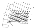
本発明の実施例を以下に図を用いて説明する。図1はコネクタにはんだ5および導電線4を配置した様子を示した図である。はんだ5はコンタクト2と導電線4の間に配置する。
Embodiments of the present invention will be described below with reference to the drawings. FIG. 1 is a diagram showing a state in which solder 5 and
このときはんだはペースト、或いはボールのような状態で供給される。図1ではペースト状のはんだを示している。はんだ5はコンタクト2上に配置され、図に示したように導電線4をコンタクト上に配置したとき、はんだ5はコンタクト2と導電線4の間に位置する。このコンタクトはいわゆるMIDによりハウジング上に形成されており、ハウジング上に形成された貫通口を経由して、またはハウジング上面から側面を経由して下面に至るように形成されている。MIDではこのような立体形状のコンタクトを形成することが容易であり、本発明の方法と組み合わせることで、より有効な効果が達成されることとなる。
At this time, the solder is supplied in the state of a paste or a ball. FIG. 1 shows paste solder. The
このようにコネクタ1に導電線4、はんだ5を配置した後、はんだ付けの作業に入る。はんだ付けは光ビームが全てのはんだに照射されるように横方向に走査することによって行う。ここで光ビームは例えばソフトビーム(登録商標)などが使用できる。
After arranging the
このとき、光ビームははんだを溶融させるだけのエネルギーを持っているため、該光ビームを走査したときコンタクトが形成されている領域以外に光ビームが当たると変形などが生じてしまう。特にコネクタの形状によっては光源に近い部分が変形する。従って不要な部分に光ビームが照射されないようにマスクを設置する。 At this time, since the light beam has sufficient energy to melt the solder, when the light beam strikes the region other than the region where the contact is formed, deformation or the like occurs. In particular, depending on the shape of the connector, the portion close to the light source is deformed. Therefore, a mask is installed so that a light beam is not irradiated to an unnecessary part.
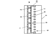
図2は導電線の軸方向から見たコネクタ全体の正面図である。コネクタ1に導電線4が配置され、はんだ5が供給されている。ここで図1、2では、はんだは一部のコンタクト2または導電線4に供給されいるように示されているが、すべてのコンタクト2、または導電線4に供給されることは明白である。この段階でコネクタ1上にはマスク7が設置される。コネクタ1にマスク7が設置されている状態の参照符号11で示された部分の拡大図を図3に示した。
FIG. 2 is a front view of the entire connector as seen from the axial direction of the conductive wire.
図3を見るとマスク7によって遮蔽される領域はコンタクト領域8を区画する壁部6、およびコネクタ1の光源に近い部分10の上部であることがわかる。しかしながら遮蔽される領域は本実施例に限定されるものではなく、光ビームにより変形等の損傷を受けない部分は遮蔽されなくてもよい。また、はんだ付けを行うコンタクト領域8の上部にはマスク7に窓9が開口しており、それ以外の部分は光ビームを遮蔽するようになっている。この窓9を通って光ビームがコンタクト領域8に照射される。よって光ビームは連続的に出力され、各はんだ5全てに光ビームが照射されるように走査することが出来る。このときマスク7は同軸線を押圧して固定するための治具としても機能する。
As can be seen from FIG. 3, the region shielded by the
このようにして光ビームを用いたはんだ付けを行うことが出来、携帯電話に使用されるコネクタのように非常に小さな構造であっても、また物理的な取り扱いが困難な場合でも素早く確実にはんだ付けを行うことが出来る。さらには、コネクタ1に形成されるコンタクト2は、別の工程でMIDによって形成されることが望ましい。これによって、小さく立体的な構造のコンタクトで、はんだ付け作業が困難なものでも、はんだ装置のはんだ付け手段との接触を必要としないことから、導線とコンタクトとの接続を容易に行うことが出来る。
In this way, it is possible to perform soldering using a light beam. Even if it is a very small structure such as a connector used in a mobile phone or when physical handling is difficult, soldering can be performed quickly and reliably. Can be attached. Furthermore, the
本実施例ではマスク7の材料として鉄を想定している。これは例えば光ビームとしてソフトビーム(登録商標)を用いる場合、該ソフトビームの光源としてキセノン光源が用いられているため、この光源に適した材料として鉄を用いている。しかしながらこれに限定されるものではなく、光ビームを遮断することが出来る材料であれば金属、プラスチック、樹脂、その他の材料も含めてすべて本発明の範囲に含まれる。
In this embodiment, iron is assumed as the material of the
本発明ではさらにコネクタ1の構造として隣同士のコンタクト領域8を区画する壁部6の構造も提供する。図1を見ると壁部6は導電線4の軸方向に沿って形成されている。図3に示したように壁部6のハウジング1からの高さは導電線4の直径より大きくなっている。本発明によればこの壁部6の高さは少なくとも導電線4の直径の約2倍である。この高さにすることによって、光ビームによりはんだが溶融した場合、はんだの飛散による近隣のコンタクトとの短絡を確実に防止することが出来る。
The present invention also provides a structure of the
1 コネクタ
2 コンタクト
3 同軸線
4 導電線
5 はんだ
6 壁部
7 マスク
8 コンタクト領域
9 窓
10 コネクタの光源に近い部分
DESCRIPTION OF
Claims (10)
コンタクトが形成されている領域に導電線を設置する段階と、
コンタクトが形成されている領域にはんだを供給する段階と、
コネクタを部分的に光ビームから遮蔽するマスクを設置する段階と、
光ビームを照射してはんだを溶融させ導電線とコンタクトを接続する段階とを含む接続方法。 A method of connecting a conductive line and a contact by a light beam,
Installing conductive wires in the area where the contacts are formed;
Supplying solder to the area where the contacts are formed;
Installing a mask that partially shields the connector from the light beam;
Connecting the conductive wire and the contact by irradiating the light beam to melt the solder.
Priority Applications (7)
| Application Number | Priority Date | Filing Date | Title |
|---|---|---|---|
| JP2004107905A JP2005294055A (en) | 2004-03-31 | 2004-03-31 | Light beam joining method |
| EP05728835A EP1737086A1 (en) | 2004-03-31 | 2005-03-31 | Light beam bonding |
| CNA200580009894XA CN1938912A (en) | 2004-03-31 | 2005-03-31 | beam splicing |
| TW094110336A TW200541426A (en) | 2004-03-31 | 2005-03-31 | Light beam bonding |
| PCT/JP2005/006285 WO2005096458A1 (en) | 2004-03-31 | 2005-03-31 | Light beam bonding |
| US10/593,765 US20070278278A1 (en) | 2004-03-31 | 2005-03-31 | Light Beam Bonding |
| MXPA06011220A MXPA06011220A (en) | 2004-03-31 | 2005-03-31 | Light beam bonding. |
Applications Claiming Priority (1)
| Application Number | Priority Date | Filing Date | Title |
|---|---|---|---|
| JP2004107905A JP2005294055A (en) | 2004-03-31 | 2004-03-31 | Light beam joining method |
Publications (1)
| Publication Number | Publication Date |
|---|---|
| JP2005294055A true JP2005294055A (en) | 2005-10-20 |
Family
ID=35064105
Family Applications (1)
| Application Number | Title | Priority Date | Filing Date |
|---|---|---|---|
| JP2004107905A Withdrawn JP2005294055A (en) | 2004-03-31 | 2004-03-31 | Light beam joining method |
Country Status (7)
| Country | Link |
|---|---|
| US (1) | US20070278278A1 (en) |
| EP (1) | EP1737086A1 (en) |
| JP (1) | JP2005294055A (en) |
| CN (1) | CN1938912A (en) |
| MX (1) | MXPA06011220A (en) |
| TW (1) | TW200541426A (en) |
| WO (1) | WO2005096458A1 (en) |
Family Cites Families (6)
| Publication number | Priority date | Publication date | Assignee | Title |
|---|---|---|---|---|
| JPH05167241A (en) * | 1991-11-20 | 1993-07-02 | Hitachi Ltd | Laser reflow jig |
| JP3438932B2 (en) * | 1994-02-18 | 2003-08-18 | オリンパス光学工業株式会社 | Imaging device assembling method |
| JPH10242595A (en) * | 1997-02-26 | 1998-09-11 | Brother Ind Ltd | Circuit board |
| JP2001244640A (en) * | 2000-02-25 | 2001-09-07 | Ibiden Co Ltd | Method of manufacturing multilayer printed wiring board and multilayer printed wiring board |
| JP2001244030A (en) * | 2000-02-29 | 2001-09-07 | Fci Japan Kk | Plug connector |
| JP4026439B2 (en) * | 2002-07-31 | 2007-12-26 | 日立電線株式会社 | Terminal connection method of micro coaxial cable assembly |
-
2004
- 2004-03-31 JP JP2004107905A patent/JP2005294055A/en not_active Withdrawn
-
2005
- 2005-03-31 MX MXPA06011220A patent/MXPA06011220A/en not_active Application Discontinuation
- 2005-03-31 US US10/593,765 patent/US20070278278A1/en not_active Abandoned
- 2005-03-31 TW TW094110336A patent/TW200541426A/en unknown
- 2005-03-31 CN CNA200580009894XA patent/CN1938912A/en active Pending
- 2005-03-31 EP EP05728835A patent/EP1737086A1/en not_active Withdrawn
- 2005-03-31 WO PCT/JP2005/006285 patent/WO2005096458A1/en not_active Ceased
Also Published As
| Publication number | Publication date |
|---|---|
| WO2005096458A1 (en) | 2005-10-13 |
| MXPA06011220A (en) | 2007-04-02 |
| EP1737086A8 (en) | 2007-02-21 |
| TW200541426A (en) | 2005-12-16 |
| EP1737086A1 (en) | 2006-12-27 |
| WO2005096458B1 (en) | 2005-12-08 |
| CN1938912A (en) | 2007-03-28 |
| US20070278278A1 (en) | 2007-12-06 |
Similar Documents
| Publication | Publication Date | Title |
|---|---|---|
| JP6728917B2 (en) | Method of manufacturing electronic circuit module | |
| JP6265852B2 (en) | connector | |
| CN103311698B (en) | There is electrical equipment and the communications component of electric contact array | |
| KR101015793B1 (en) | Wire harness | |
| CN108335821B (en) | coil element | |
| US20070193991A1 (en) | Method of soldering wiring members by laser beam irradiation | |
| JPH1131876A (en) | Circuit board | |
| US20160020577A1 (en) | Semiconductor laser device | |
| CN1235076C (en) | Optical connector and element | |
| JP2005294055A (en) | Light beam joining method | |
| JP2005158883A (en) | Circuit board | |
| JP5712090B2 (en) | Manufacturing method of electronic equipment | |
| KR20070023688A (en) | Light beam junction | |
| JP2006005107A (en) | Circuit structure | |
| JP5118713B2 (en) | CIRCUIT MODULE, ELECTRONIC DEVICE HAVING THE SAME, AND CIRCUIT MODULE MANUFACTURING METHOD | |
| CN104604342A (en) | Circuit board assembly and terminal with circuit board assembly | |
| TW200420440A (en) | Electrical interconnect assemblies and methods of forming same | |
| JP2006303354A (en) | Printed-wiring board and method for joining the same | |
| KR20170076653A (en) | Printed circuit board, method for producing printed circuit board, and method for bonding conductive member | |
| KR101937281B1 (en) | Connection structure for coaxial cable | |
| JP2013219404A (en) | Method for manufacturing antenna component | |
| JP6944028B2 (en) | Board connection structure and conductor connection method | |
| JP4569361B2 (en) | Circuit board and laser soldering method | |
| JP2007123531A (en) | Printed circuit board and printed circuit board using the same | |
| JPH05315778A (en) | Electronic parts mounting board provided with heat sink |
Legal Events
| Date | Code | Title | Description |
|---|---|---|---|
| A761 | Written withdrawal of application |
Free format text: JAPANESE INTERMEDIATE CODE: A761 Effective date: 20070413 |