JP2005293813A - Nand flash memory device and method of reading the same - Google Patents
Nand flash memory device and method of reading the same Download PDFInfo
- Publication number
- JP2005293813A JP2005293813A JP2004192821A JP2004192821A JP2005293813A JP 2005293813 A JP2005293813 A JP 2005293813A JP 2004192821 A JP2004192821 A JP 2004192821A JP 2004192821 A JP2004192821 A JP 2004192821A JP 2005293813 A JP2005293813 A JP 2005293813A
- Authority
- JP
- Japan
- Prior art keywords
- local
- signal
- source
- voltage
- string
- Prior art date
- Legal status (The legal status is an assumption and is not a legal conclusion. Google has not performed a legal analysis and makes no representation as to the accuracy of the status listed.)
- Pending
Links
- 238000000034 method Methods 0.000 title claims abstract description 12
- 230000005540 biological transmission Effects 0.000 claims description 21
- 238000001514 detection method Methods 0.000 claims description 20
- 230000008878 coupling Effects 0.000 description 4
- 238000010168 coupling process Methods 0.000 description 4
- 238000005859 coupling reaction Methods 0.000 description 4
- 238000010586 diagram Methods 0.000 description 4
- 238000012544 monitoring process Methods 0.000 description 3
- 230000007423 decrease Effects 0.000 description 2
- 239000004065 semiconductor Substances 0.000 description 2
- 239000000758 substrate Substances 0.000 description 2
- 230000002411 adverse Effects 0.000 description 1
- 230000015556 catabolic process Effects 0.000 description 1
- 230000003247 decreasing effect Effects 0.000 description 1
- 230000000694 effects Effects 0.000 description 1
- 230000010354 integration Effects 0.000 description 1
- 150000002500 ions Chemical class 0.000 description 1
- 230000014759 maintenance of location Effects 0.000 description 1
- 238000012986 modification Methods 0.000 description 1
- 230000004048 modification Effects 0.000 description 1
- 238000005070 sampling Methods 0.000 description 1
Images
Classifications
-
- G—PHYSICS
- G11—INFORMATION STORAGE
- G11C—STATIC STORES
- G11C16/00—Erasable programmable read-only memories
- G11C16/02—Erasable programmable read-only memories electrically programmable
- G11C16/06—Auxiliary circuits, e.g. for writing into memory
- G11C16/26—Sensing or reading circuits; Data output circuits
-
- G—PHYSICS
- G11—INFORMATION STORAGE
- G11C—STATIC STORES
- G11C16/00—Erasable programmable read-only memories
- G11C16/02—Erasable programmable read-only memories electrically programmable
- G11C16/04—Erasable programmable read-only memories electrically programmable using variable threshold transistors, e.g. FAMOS
- G11C16/0483—Erasable programmable read-only memories electrically programmable using variable threshold transistors, e.g. FAMOS comprising cells having several storage transistors connected in series
-
- G—PHYSICS
- G11—INFORMATION STORAGE
- G11C—STATIC STORES
- G11C16/00—Erasable programmable read-only memories
- G11C16/02—Erasable programmable read-only memories electrically programmable
- G11C16/06—Auxiliary circuits, e.g. for writing into memory
- G11C16/24—Bit-line control circuits
Landscapes
- Engineering & Computer Science (AREA)
- Microelectronics & Electronic Packaging (AREA)
- Read Only Memory (AREA)
- Semiconductor Memories (AREA)
- Non-Volatile Memory (AREA)
Abstract
Description
本発明は、NANDフラッシュメモリ素子及びその読み取り方法に関し、特に、素子の漏れ電流を減少させることのできるNANDフラッシュメモリ素子に関する。 The present invention relates to a NAND flash memory device and a reading method thereof, and more particularly, to a NAND flash memory device capable of reducing a leakage current of the device.
NAND型フラッシュ素子は、ドレイン選択トランジスタとソース選択トランジスタとの間に16個または32個単位でセルがストリング(String)形態で直列接続している。同一ワードラインを共有しているセルストリングをグループ化して一つのブロックと定義する。 In the NAND flash device, cells are connected in series in a string form in units of 16 or 32 between a drain selection transistor and a source selection transistor. Cell strings sharing the same word line are grouped and defined as one block.
ブロックに印加される電圧の状態によって、読み出し動作のために選択されたブロックと選択されないブロックとに分けられる。 Depending on the state of the voltage applied to the block, the block is divided into a block selected for the read operation and a block not selected.
まず、読み出し動作時選択されたブロックに印加される電圧状態を述べると、Xデコーダを介して選択されたワードラインには0Vを印加し、パスワードライン、ドレイン選択トランジスタ及びソース選択トランジスタには4.5Vの電圧を印加する。共通ソースラインとバルクとには0Vを印加し、ビットラインには1Vの電圧を印加する。 First, the voltage state applied to the block selected during the read operation will be described. 0V is applied to the word line selected through the X decoder, and 4 V is applied to the password line, drain selection transistor, and source selection transistor. A voltage of 5V is applied. A voltage of 0 V is applied to the common source line and the bulk, and a voltage of 1 V is applied to the bit line.
次に、選択されないブロックを述べると、Xデコーダを介して全体ワードライン、ドレイン選択トランジスタ及びソース選択トランジスタをフローティングさせる。ソース選択トランジスタは、選択されたブロックと選択されないブロックとが電気的に接続されている。選択されないブロックのソース選択トランジスタには4.5Vの電圧が印加されることができる。共通ソースライン、バルク及びビットラインに印加される電圧状態は選択されたブロックと同じである。 Next, to describe a non-selected block, the entire word line, the drain selection transistor, and the source selection transistor are floated through the X decoder. In the source selection transistor, a selected block and an unselected block are electrically connected. A voltage of 4.5 V can be applied to the source selection transistors of the unselected blocks. The voltage state applied to the common source line, bulk, and bit line is the same as the selected block.
このような電圧印加時、選択されないブロックのドレイン選択トランジスタ及びソース選択トランジスタにより発生した漏れ電流により素子の動作に悪影響を及ぼしている。一般にストリング単位のNANDアレイは根本的なオン電流(On-Current)が200ないし400nA程度で非常に小さい。短いセンシングタイム(Sensing Time)を持っていくためには、選択されないブロックの漏れ電流が漏れないように制御しなければならない。 When such a voltage is applied, the leakage current generated by the drain selection transistor and the source selection transistor in the unselected block adversely affects the operation of the element. In general, a string-unit NAND array has a very small on-current of about 200 to 400 nA. In order to have a short sensing time (Sensing Time), it is necessary to control so that the leakage current of the non-selected block does not leak.
また、NANDフラッシュセルは接合漏れ(Junction Leakage)によるプログラムディスターブ(Program Disturb)発生を防止するため、8V電圧において数pAの漏れ電流だけを許容する。したがって、ゲート長さが0.1umのセルと0.18umの選択トランジスタにもディップ接合(DeepJunction)構造を形成しなければならない。これにより接合部と接合部(Junction To Junction)との間の漏れ、すなわち、パンチスルー(Punch-Thorough)に弱い問題が発生する。 In addition, the NAND flash cell allows only a leakage current of several pA at 8V voltage in order to prevent occurrence of program disturb due to junction leakage. Therefore, a dip junction structure must also be formed in a cell having a gate length of 0.1 μm and a selection transistor having a 0.18 μm length. As a result, there is a problem that leakage between the junction and the junction (Junction To Junction), that is, punch-through is weak.
したがって、本発明は上述した問題点に鑑みてなされたものであって、その目的とするところは、読み出し動作時選択トランジスタのソースサイド抵抗を大きくして漏れ電流を減少させることのできるNANDフラッシュメモリ素子及びその読み出し方法を提供する。 Accordingly, the present invention has been made in view of the above-described problems, and an object of the present invention is to provide a NAND flash memory capable of reducing a leakage current by increasing a source side resistance of a selection transistor during a read operation. An element and a reading method thereof are provided.
本発明に係るローカルストリング選択信号によって複数のビットライン信号を伝送するストリング選択部と、ローカルソース選択信号によって共通ソースライン信号を伝送するソース選択部と、複数のビットライン信号、共通ソースライン信号及び複数のローカルワードライン信号によって所定のデータを格納するセルストリング部とを含むセルブロックと、動作信号によってグローバルストリング選択信号、グローバルソース選択信号及び複数のグローバルワードライン信号をそれぞれ前記ローカルストリング選択信号、前記ローカルソース選択信号及び前記複数のローカルワードライン信号に伝送するXデコーダ部と、所定の制御信号によって前記ローカルストリング選択信号及び前記ローカルソース選択信号に接地電源信号を印加するスイッチ部とを備えるNANDフラッシュメモリ素子を提供する。 A string selection unit that transmits a plurality of bit line signals using a local string selection signal, a source selection unit that transmits a common source line signal using a local source selection signal, a plurality of bit line signals, a common source line signal, and A cell block including a cell string unit that stores predetermined data by a plurality of local word line signals, and a global string selection signal, a global source selection signal, and a plurality of global word line signals by an operation signal, respectively, An X decoder for transmitting to the local source selection signal and the plurality of local word line signals, and applying a ground power signal to the local string selection signal and the local source selection signal according to a predetermined control signal. Providing a NAND flash memory device and a switch unit.
また、複数のビットラインに接続された複数のストリング選択トランジスタと共通ソースラインに接続された複数のソース選択トランジスタとの間に直列接続された複数のセルストリングと、前記複数のストリング選択トランジスタのゲート端子に接続されたローカルストリング選択ラインと、前記複数のソース選択トランジスタのゲート端子に接続されたローカルソース選択ライン及び前記セルストリング内のセル各々のゲート端子に接続された複数のローカルワードラインとを含む複数のセルブロックと、それぞれ動作電圧によって駆動しグローバルストリング選択ラインと前記ローカルストリング選択ラインとに接続されたストリング伝送トランジスタと、グローバルソース選択ラインと前記ローカルソース選択ラインとに接続されたソース伝送トランジスタ、複数のグローバルワードラインと前記複数のローカルワードラインとに接続された複数のワードライン伝送トランジスタとを含むXデコーダ部と、それぞれ制御電圧によって駆動し接地電源と前記ローカルストリング選択ラインとに接続されたストリング放電トランジスタと、接地電源と前記ローカルソース選択ラインとに接続されたソース放電トランジスタとを含むスイッチ部と、読み出し動作信号によって前記ビットラインに検出電圧を印加し、前記検出電圧の状態によってセルのプログラム及び消去状態を判断するページバッファ部とを備えるNANDフラッシュメモリ素子において、前記Xデコーダ部にグローバルストリング選択電圧、グローバルソース選択電圧及び選択されない複数のワードラインにはパス電圧を印加し、選択されたワードラインには読み出し電圧を印加し、選択された前記セルブロックと接続された前記Xデコーダ部にロジックハイの動作電圧を印加し、選択されない前記セルブロックと接続された前記Xデコーダ部にロジックローの動作電圧を印加するステップと、選択された前記セルブロックと接続された前記スイッチ部にロジックローの制御電圧を印加し、選択されない前記セルブロックと接続された前記スイッチ部にロジックハイの制御電圧を印加するステップと、前記共通ソースラインとバルクとに接地電圧を印加し、前記ページバッファを介して選択された前記ビットラインに検出電圧を印加した後、前記検出電圧の変化をセンシングするステップとを備えることを特徴とするNANDフラッシュメモリ素子の読み取り方法を提供する。 A plurality of cell strings connected in series between a plurality of string selection transistors connected to a plurality of bit lines and a plurality of source selection transistors connected to a common source line, and gates of the plurality of string selection transistors A local string selection line connected to a terminal; a local source selection line connected to a gate terminal of the plurality of source selection transistors; and a plurality of local word lines connected to a gate terminal of each cell in the cell string. A plurality of cell blocks including a string transmission transistor driven by an operating voltage and connected to the global string selection line and the local string selection line; and connected to the global source selection line and the local source selection line. An X decoder unit including a source transmission transistor, a plurality of global word lines and a plurality of word line transmission transistors connected to the plurality of local word lines, and a ground power source and the local string selection line driven by a control voltage, respectively. A detection unit configured to apply a detection voltage to the bit line according to a read operation signal, and a switch unit including a string discharge transistor connected to the ground power source and a source discharge transistor connected to a ground power source and the local source selection line. In a NAND flash memory device having a page buffer unit for determining a programmed and erased state of a cell according to the state of the X decoder, the X decoder unit includes a global string selection voltage, a global source selection voltage, and a plurality of unselected word lines. A read voltage is applied to the selected word line, a logic high operating voltage is applied to the X decoder connected to the selected cell block, and the selected cell block is connected to the unselected cell block. Applying a logic low operating voltage to the selected X decoder unit, applying a logic low control voltage to the switch unit connected to the selected cell block, and connecting to the non-selected cell block Applying a logic high control voltage to the switch unit; applying a ground voltage to the common source line and the bulk; and applying a detection voltage to the bit line selected through the page buffer; Sensing a change in a detection voltage, and reading a NAND flash memory device Provide a sampling method.
上述したように、本発明は読み出し動作時、選択されないセルブロックのストリング選択のためのトランジスタとソース選択のためのトランジスタとに接地電源を印加することによって、ドレイン選択ラインの抵抗を増加させてバックバイアス効果による漏れ電流を防止できる。 As described above, the present invention increases the resistance of the drain selection line by increasing the resistance of the drain selection line by applying a ground power source to the string selection transistor and the source selection transistor of the unselected cell block during a read operation. Leakage current due to the bias effect can be prevented.
また、ビットライン漏れ電流が減少してプログラムされたセルと消去されたセルとの間のオン/オフ電流比が増加することになって、素子のセンシングタイムが減少し、リ―ドトリップレンジが増加してデータ保損力及び読み出しディスターブによるしきい電圧変化を防止できる。 Also, the bit line leakage current is reduced, increasing the on / off current ratio between programmed and erased cells, reducing the sensing time of the device and reducing the lead trip range. The threshold voltage change due to the increase in data integrity and read disturb can be prevented.
また、しきい電圧変化に対するマージンを増加させることができ、ページバッファ変化(Page Buffer Variation)に対するマージンを増加させることができる。 In addition, a margin for a threshold voltage change can be increased, and a margin for a page buffer variation can be increased.
また、セルブロック間のソース選択トランジスタ各々を分離してソース選択ラインに独立的な電圧を印加することもでき、隣接したセルブロック間のソース選択トランジスタを電気的に接続してソース放電トランジスタの数字を低減できる。 In addition, the source selection transistors between the cell blocks can be separated and an independent voltage can be applied to the source selection line, and the source selection transistors between adjacent cell blocks can be electrically connected to each other. Can be reduced.
以下、添付した図面を参照して本発明の実施の形態をさらに詳細に説明する。 Hereinafter, embodiments of the present invention will be described in more detail with reference to the accompanying drawings.
複数のフラッシュセルがストリング形態で構成されたセルストリングのようなワードラインを共有しているストリングをグループ化して一つのブロックで構成した。このようなブロックを構成している各々のストリングは、グローバルビットラインに1024、2048のような2の倍数単位で並列接続している。また、ブロック配列は、選択トランジスタを基準としてミラー(Mirror)構造で形成されているため、選択トランジスタのストリングアウトサイド接合部(Out-Side Junction)を隣接したブロックの選択トランジスタと共有している。 Strings sharing a word line such as a cell string in which a plurality of flash cells are formed in a string form are grouped to form one block. Each string constituting such a block is connected in parallel to a global bit line in units of multiples of 2 such as 1024 and 2048. In addition, since the block arrangement is formed in a mirror structure with the selection transistor as a reference, the string outside junction (Out-Side Junction) of the selection transistor is shared with the selection transistor of the adjacent block.
高度な集積化のため、データ入出力パスであるビットラインと接続したストリング選択トランジスタには、その構成上ブロックと別にストリング選択トランジスタゲートバイアスを印加することが効果的である。また、共通ソースラインと接続したソース選択トランジスタは隣接したソース選択トランジスタとゲートバイアス(Gate Bias)とを共有したり、別のゲートバイアスを印加されることが好ましい。 In order to achieve a high degree of integration, it is effective to apply a string selection transistor gate bias to the string selection transistor connected to the bit line which is a data input / output path separately from the block in terms of its configuration. In addition, the source selection transistor connected to the common source line preferably shares a gate bias (Gate Bias) with an adjacent source selection transistor or is applied with another gate bias.
NANDフラッシュ素子の読み取り動作時、あらゆるブロックはソースラインには0Vを印加し、ビットラインには最大1.3V程度の電圧を印加する。この場合、ビットラインによる漏れ電流をほぼ無視できるが、ストリング選択トランジスタあるいはソース選択トランジスタのソース/ドレイン間漏れ電流は無視できない程度となる。また、ビットラインには1024個のストリングが並列接続しているため、漏れ電流は1024倍に増幅されて流れるようになる。 During the reading operation of the NAND flash device, all the blocks apply 0 V to the source line and apply a maximum voltage of 1.3 V to the bit line. In this case, the leakage current due to the bit line can be almost ignored, but the leakage current between the source / drain of the string selection transistor or the source selection transistor cannot be ignored. In addition, since 1024 strings are connected in parallel to the bit line, the leakage current is amplified by 1024 times and flows.
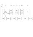
図1は、選択されないブロックのストリング選択トランジスタには0Vのゲート電圧を印加し、ソース選択トランジスタはフローティングさせた状態の概念図である。 FIG. 1 is a conceptual diagram showing a state in which a gate voltage of 0 V is applied to a string selection transistor in an unselected block and a source selection transistor is left floating.
図1を参照すれば、セルの読み取り動作時選択されないブロックのストリング選択トランジスタT1にだけ0Vのゲート電圧を印加し、ソース選択トランジスタT10とセルストリングのゲートをフローティングさせる場合は次の通りである。セルストリング内のセルが消去された状態であれば、大部分のセルが-7ないし-9V程度のしきい電圧(Vt=-9)を有する。この場合、フローティングゲートはポジティブチャージングされている。したがって、容量性カップリング(CapacitiveCoupling)を考慮すれば、フローティングゲートの電位(Potential)が4.0ないし5.0V程度となって、セルのワードラインがフローティングされていても事実上セルが完全にターンオンされた状態となる。 Referring to FIG. 1, a gate voltage of 0V is applied only to the string selection transistor T1 of a block that is not selected during a cell read operation, and the source selection transistor T10 and the gate of the cell string are floated as follows. If the cells in the cell string are erased, most cells have a threshold voltage (Vt = -9) of about -7 to -9V. In this case, the floating gate is positively charged. Therefore, in consideration of capacitive coupling, the potential of the floating gate (Potential) is about 4.0 to 5.0 V, and even if the cell word line is floating, the cell is practically completely Turned on.
また、ソース選択トランジスタT10も隣接したセル、ソースライン及び半導体基板間の容量性カップリングにより約0.4ないし0.5V程度の電位を持つようになる。これによりソース選択トランジスタはほぼターンオンされた状態となる。 The source selection transistor T10 also has a potential of about 0.4 to 0.5V due to capacitive coupling between adjacent cells, source lines, and the semiconductor substrate. As a result, the source selection transistor is almost turned on.
上述したことにより、ストリング選択トランジスタT1のソースサイドであるソース選択トランジスタT10からセルストリング全体までの直列抵抗が大きく減少するので漏れ電流が流れるようになる。したがって、セルのターンオン状態を防止できなくても、ソース選択トランジスタのほぼターンオンされた状態のみを予防できれば、ストリング選択トランジスタのソースサイド抵抗を増加させてストリング単位の漏れ電流を減少させることができる。 As described above, since the series resistance from the source selection transistor T10, which is the source side of the string selection transistor T1, to the entire cell string is greatly reduced, a leakage current flows. Therefore, even if the turn-on state of the cell cannot be prevented, if only the source selection transistor is almost turned on can be prevented, the source-side resistance of the string selection transistor can be increased and the leakage current of the string unit can be reduced.
これに関し素子の構成とそれにともなう素子の読み取り動作に関し図面を参照して詳細に説明する。 In this regard, the configuration of the element and the element reading operation associated therewith will be described in detail with reference to the drawings.
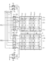
図2は、本発明に係るNANDフラッシュメモリ素子の回路図である。 FIG. 2 is a circuit diagram of a NAND flash memory device according to the present invention.
図2を参照すれば、本発明のNANDフラッシュメモリ素子はローカルストリング選択信号DSLによって複数のビットライン信号BLを伝送するストリング選択部120と、ローカルソース選択信号SSLによって共通ソースライン信号SLを伝送するソース選択部130と、複数のビットライン信号BL、共通ソースライン信号SL及び複数のローカルワードライン信号WLOないしWLnによって所定のデータを格納するセルストリング部110を含むセルブロック100と、動作信号BLKWLによってグローバルストリング選択信号GDSL、グローバルソース選択信号GSSL及び複数のグローバルワードライン信号GWLないしGWLnをそれぞれローカルストリング選択信号DSL、ローカルソース選択信号SSL及び複数のローカルワードライン信号WL0ないしWLnに伝送するXデコーダ部200と、所定の制御信号CSによってローカルストリング選択信号DSL及びローカルソース選択信号SSLに接地電源信号を印加するスイッチ部300とを備える。 Referring to FIG. 2, the NAND flash memory device of the present invention transmits a plurality of bit line signals BL by a local string selection signal DSL and a common source line signal SL by a local source selection signal SSL. A source selection unit 130, a cell block 100 including a cell string unit 110 for storing predetermined data by a plurality of bit line signals BL, a common source line signal SL, and a plurality of local word line signals WLO to WLn, and an operation signal BLKWL The global string selection signal GDSL, the global source selection signal GSSL, and the plurality of global word line signals GWL to GWLn are respectively converted into the local string selection signal DSL, the local source selection signal SSL, and the plurality of global word line selection signals SSL. Provided to no local word line signals WL0 and X decoder 200 to be transmitted to WLn, and a switch portion 300 for applying a ground power supply signal to a local string select signal DSL and the local source selection signal SSL by a predetermined control signal CS.
読み出し動作信号(図示せず)によって前記ビットラインBLに検出電圧を印加し、前記検出電圧の状態によってセルのプログラム及び消去状態をセンシングするページバッファ部(図示せず)をさらに備えることができる。 A page buffer unit (not shown) that applies a detection voltage to the bit line BL according to a read operation signal (not shown) and senses a program and erase state of the cell according to the state of the detection voltage may be further included.
セルブロック100のストリング選択部120は、複数のビットラインBLにそれぞれ接続されローカルストリング選択信号SSLによってビットラインBL信号を伝送する複数のストリング選択トランジスタT1ないしTnを備える。ソース選択部130は、共通ソースラインSLに接続されローカルソース選択信号SSLによって共通ソースラインSL信号を伝送する複数のソース選択トランジスタT100ないしTmを備える。 The string selection unit 120 of the cell block 100 includes a plurality of string selection transistors T1 to Tn that are connected to the plurality of bit lines BL and transmit the bit line BL signal using a local string selection signal SSL. The source selection unit 130 includes a plurality of source selection transistors T100 to Tm that are connected to the common source line SL and transmit the common source line SL signal using the local source selection signal SSL.
セルストリング部は直列接続された複数のセルが複数のストリング選択トランジスタT1ないしTnと複数のソース選択トランジスタT100ないしTmとの間にそれぞれ接続された複数のセルストリングを含み、複数のセルストリング内の同一位置にあるセルのゲート各々にローカルワードラインWLが接続され複数のビットライン信号BL、共通ソースライン信号SSL及び複数のローカルワードライン信号WL0ないしWLnによって所定のデータを格納したり消去する。 The cell string portion includes a plurality of cell strings in which a plurality of cells connected in series are respectively connected between the plurality of string selection transistors T1 to Tn and the plurality of source selection transistors T100 to Tm. A local word line WL is connected to each gate of the cells at the same position, and predetermined data is stored or erased by a plurality of bit line signals BL, a common source line signal SSL, and a plurality of local word line signals WL0 to WLn.
Xデコーダ部200は、動作信号BLKWLによってそれぞれグローバルストリング選択信号GDSLをローカルストリング選択信号GSLに伝送するストリング伝送トランジスタ210と、グローバルソース選択信号GSSLをローカルソース選択信号SSLに伝送するソース伝送トランジスタ230と、複数のグローバルワードライン信号GWL0ないしGWLmを複数のローカルワードライン信号WL0ないしWLnに伝送する複数のワードライン伝送トランジスタ220とを備える。 The X decoder unit 200 includes a string transmission transistor 210 that transmits the global string selection signal GDSL to the local string selection signal GSL according to the operation signal BLKWL, and a source transmission transistor 230 that transmits the global source selection signal GSSL to the local source selection signal SSL. And a plurality of word line transmission transistors 220 for transmitting a plurality of global word line signals GWL0 to GWLm to a plurality of local word line signals WL0 to WLn.
スイッチ部300は、制御信号CSによってそれぞれローカルストリング選択信号DSLに接地電源を伝送するストリング放電トランジスタ310と、ローカルソース選択信号SSLに接地電源を伝送するソース放電トランジスタ320とを備える。 The switch unit 300 includes a string discharge transistor 310 that transmits ground power to the local string selection signal DSL according to a control signal CS, and a source discharge transistor 320 that transmits ground power to the local source selection signal SSL.
この場合、隣接した前記セルブロック100aと100bの前記ソース選択部130aと130bに同じ前記ローカルソース選択信号SSLが印加されるように、隣接した前記セルブロック間100aと100bの前記ソース選択部130aと130bを電気的に接続したり、隣接した前記セルブロック100aと100bの前記ソース選択部130aと130bにそれぞれ独立された前記ローカルソース選択信号SSLが印加されるように、隣接した前記セルブロック間100aと100bの前記ソース選択部130aと130bを電気的に分離することができる。また、2個以上のソース選択部130に同じローカルソース選択信号SSLが印加されるように、ソース選択部130を電気的に接続できる。
In this case, the
複数のストリング選択トランジスタT1ないしTnと複数のソース選択トランジスタT100ないしTmとは、NMOSトランジスタを使用することが好ましい。複数のストリング選択トランジスタT1ないしTnと複数のソース選択トランジスタT100ないしTmのうち、最初のトランジスタT1及びT100らの間に複数のセルストリングのうち最初のセルストリングが接続される。複数のセルストリングのうち、最初のセルらは最初のワードライン信号WL0によって動作する。セルストリング110に16の2の倍数個数ぐらいのセルが直列接続されることが好ましい。 The plurality of string selection transistors T1 to Tn and the plurality of source selection transistors T100 to Tm are preferably NMOS transistors. The first cell string among the plurality of cell strings is connected between the first transistors T1 and T100 among the plurality of string selection transistors T1 to Tn and the plurality of source selection transistors T100 to Tm. Among the plurality of cell strings, the first cells are operated by the first word line signal WL0. It is preferable that as many cells as multiples of 2 are connected in series to the cell string 110.
ストリング伝送トランジスタ210、ソース伝送トランジスタ230と複数のワードライン伝送トランジスタ220として、1ないし25Vの電圧でも動作が可能な高電圧NMOSトランジスタを使用することが好ましい。すなわち、20V以上の接合ブレークダウン電圧を有するトランジスタを使用することが効果的である。また、上述したトランジスタとしてイオンが注入されない半導体基板上に形成されるネガティブ高電圧トランジスタを使用することが好ましい。 As the string transmission transistor 210, the source transmission transistor 230, and the plurality of word line transmission transistors 220, it is preferable to use high voltage NMOS transistors that can operate even at a voltage of 1 to 25V. That is, it is effective to use a transistor having a junction breakdown voltage of 20V or more. Moreover, it is preferable to use a negative high voltage transistor formed on a semiconductor substrate into which ions are not implanted as the above-described transistor.
ストリング放電トランジスタ310とソース放電トランジスタ320として、高電圧NMOSトランジスタまたは一般NMOSトランジスタを使用することが好ましい。 A high voltage NMOS transistor or a general NMOS transistor is preferably used as the string discharge transistor 310 and the source discharge transistor 320.
本発明のNANDフラッシュ素子においては、1024の2の倍数個数ぐらいのセルブロック100が位置していることが好ましい。また、上述したように少なくとも2個以上のソース選択トランジスタ間のゲート端子を一つのラインで接続することもでき、それぞれ分離されたラインで接続することもできる。ゲート端子を一つのラインで接続する場合、ソース放電トランジスタの数字を減らすことができ、それぞれ分離されたラインで接続する場合、独立的な電圧を印加できる。 In the NAND flash device of the present invention, it is preferable that approximately 1024 cell blocks 100 are located. Further, as described above, the gate terminals between at least two source selection transistors can be connected by one line, or can be connected by separate lines. When the gate terminals are connected by a single line, the number of source discharge transistors can be reduced, and when they are connected by separate lines, an independent voltage can be applied.
上述した構成を有する本発明において、選択されたセルブロック内の所定のセル内のデータを読み出すための過程を説明すれば次の通りである。この場合、選択されたセルブロックを図2の100aとし、選択されないセルブロックを図1の100bとして説明する。 In the present invention having the above-described configuration, a process for reading data in a predetermined cell in a selected cell block will be described as follows. In this case, the selected cell block will be described as 100a in FIG. 2, and the non-selected cell block will be described as 100b in FIG.
複数のビットラインBL0ないしBLnに接続された複数のストリング選択トランジスタT1ないしTnと共通ソースラインSLに接続された複数のソース選択トランジスタT100ないしTmとの間に直列接続された複数のセルストリング110、前記複数のストリング選択トランジスタT1ないしTnのゲート端子に接続されたローカルストリング選択ラインDSL、前記複数のソース選択トランジスタT100ないしTmのゲート端子に接続されたローカルソース選択ラインSSL及び前記セルストリング110内のセル各々のゲート端子に接続された複数のワードラインWL0ないしWLnを含む複数のセルブロック100と、それぞれ動作電圧BLKWLによって駆動しグローバルストリング選択ラインGDSLとローカルストリング選択ラインDSLとに接続されたストリング伝送トランジスタ210、グローバルソース選択ラインGSSLとローカルソース選択ラインSSLとに接続されたソース伝送トランジスタ230及び複数のグローバルワードラインGWL0ないしGWLnと複数のローカルワードラインWL0ないしWLnとに接続された複数のワードライン伝送トランジスタ220を含むXデコーダ部200と、それぞれ制御電圧CSによって駆動し接地電源とローカルストリング選択ラインDSLとに接続されたストリング放電トランジスタ310と、接地電源とローカルソース選択ラインSSLとに接続されたソース放電トランジスタSSLを含むスイッチ部300と、読み出し動作信号(図示せず)によって前記ビットラインBLに検出電圧を印加し、前記検出電圧の状態によってセルのプログラム及び消去状態をセンシングするページバッファ部(図示せず)を含むNANDフラッシュメモリ素子において、Xデコーダ部200にグローバルストリング選択電圧、グローバルソース選択電圧、選択されない複数のワードラインにはパス電圧を印加し、選択されたワードラインには読み出し電圧を印加し、選択されたセルブロック100aと接続されたXデコーダ部200aとにロジックハイの動作電圧BLKWLaを印加し、選択されないセルブロック100bと接続されたXデコーダ部200bとにロジックローの動作電圧BLKWLbを印加する。
A plurality of cell strings 110 connected in series between a plurality of string selection transistors T1 to Tn connected to a plurality of bit lines BL0 to BLn and a plurality of source selection transistors T100 to Tm connected to a common source line SL; The local string selection line DSL connected to the gate terminals of the plurality of string selection transistors T1 to Tn, the local source selection line SSL connected to the gate terminals of the plurality of source selection transistors T100 to Tm, and the cell string 110 A plurality of cell blocks 100 including a plurality of word lines WL0 to WLn connected to the gate terminals of the respective cells, a global string selection line GDSL and a local stream driven by an operating voltage BLKWL, respectively. A string transmission transistor 210 connected to the global selection line DSL, a source transmission transistor 230 connected to the global source selection line GSSL and the local source selection line SSL, and a plurality of global word lines GWL0 to GWLn and a plurality of local word lines WL0. An X decoder unit 200 including a plurality of word line transmission transistors 220 connected to WLn, a string discharge transistor 310 driven by a control voltage CS and connected to a ground power source and a local string selection line DSL, and a ground power source And a switch unit 300 including a source discharge transistor SSL connected to the local source selection line SSL, and a detection voltage is applied to the bit line BL by a read operation signal (not shown). In a NAND flash memory device including a page buffer unit (not shown) that senses a programmed and erased state of a cell according to the detection voltage state, the X decoder unit 200 has a global string selection voltage, a global source selection voltage, a plurality of unselected A pass voltage is applied to the word line, a read voltage is applied to the selected word line, and a logic high operating voltage BLKWLa is applied to the
選択されたセルブロック100aと接続されたスイッチ部300aとにロジックローの制御電圧CSaを印加し、選択されないセルブロック100bと接続されたスイッチ部300bにロジックハイの制御電圧CSbを印加する。
A logic low control voltage CSa is applied to the
共通ソースラインSLとバルク(図示せず)に接地電圧を印加する。ページバッファを介して選択されたビットラインに検出電圧を印加した後、検出電圧の変化をセンシングする。 A ground voltage is applied to the common source line SL and the bulk (not shown). After a detection voltage is applied to the selected bit line via the page buffer, a change in the detection voltage is sensed.
本実施の形態では上述した電圧の印加順序は素子の読み取り方法によって多様に変更できる。すなわち、スイッチ部300に制御電圧を先に印加した後、Xデコーダ200に所定の電圧を印加することもできる。 In this embodiment mode, the voltage application order described above can be variously changed depending on the element reading method. That is, a predetermined voltage can be applied to the X decoder 200 after the control voltage is first applied to the switch unit 300.
グローバルストリング選択電圧、グローバルソース選択電圧及びパス電圧として4.0ないし5.0Vの電圧を使用することが好ましい。読み出し電圧として接地電圧を使用することが好ましい。 Preferably, a voltage of 4.0 to 5.0 V is used as the global string selection voltage, the global source selection voltage, and the pass voltage. It is preferable to use a ground voltage as the read voltage.
選択されたセルブロック100aと接続されたXデコーダ部200aとにロジックハイの動作電圧BLKWLaとして4.0V+2Vtないし5.0V+2Vtだけの電圧を使用することが好ましく、選択されないセルブロック100bと接続されたXデコーダ部200bにロジックローの動作電圧BLKWLbとして接地電圧を使用することが好ましい。上記のVtはXデコーダ部200内のトランジスタ等のしきい電圧を意味する。
It is preferable to use a voltage of 4.0V + 2Vt to 5.0V + 2Vt as the logic high operating voltage BLKWLa for the
検出電圧としては0.8ないし1.5Vの電圧を使用することが好ましい。 It is preferable to use a voltage of 0.8 to 1.5 V as the detection voltage.
以下、上述した説明に基づきNANDフラッシュ素子の読み出し動作時に印加される電圧を表に整理すれば次の通りである。 Hereinafter, the voltages applied during the read operation of the NAND flash device based on the above description are summarized in the following table.
表1は、本発明に係るNANDフラッシュメモリ素子に印加される電圧を示した表である。 Table 1 is a table showing voltages applied to the NAND flash memory device according to the present invention.
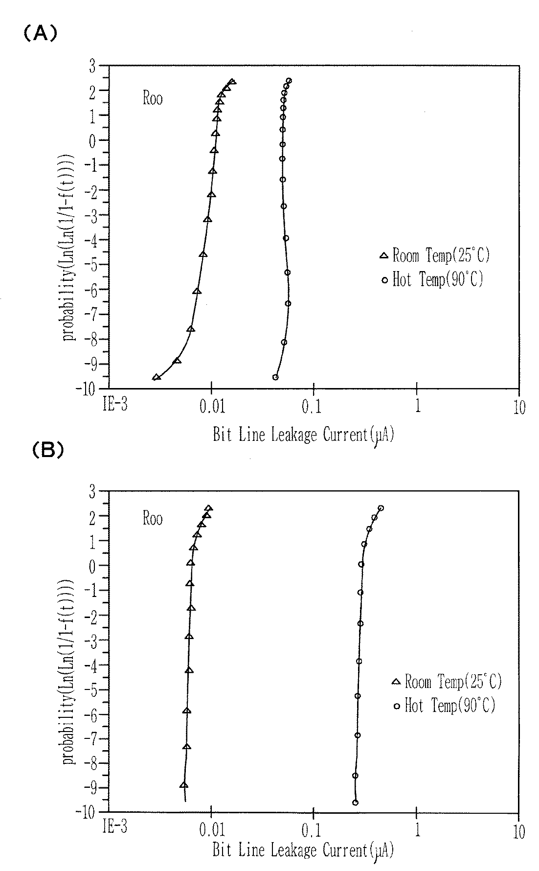
表1を参照し本発明の読み出し動作を具体的に説明すれば次の通りである。 The read operation of the present invention will be described in detail with reference to Table 1 as follows.
外部のアドレス入力を介して読み出すためのセルを選択(ワードラインとビットライン選択)し、これに伴い選択されたセルが位置しているセルブロックを選択されたセルブロック100aと定義する。
A cell to be read via an external address input is selected (word line and bit line selection), and a cell block in which the selected cell is located is defined as a selected
Xデコーダ部200のグローバルストリング選択ラインGDSL、グローバルソース選択ラインGSSL及び選択されないグローバルワードラインGWLに各々4.5Vのグローバルストリング選択電圧、グローバルソース選択電圧及びパス電圧を印加し、選択されたグローバルワードラインGWLには0Vの電圧を印加する。 A global string selection voltage, a global source selection voltage and a pass voltage of 4.5 V are applied to the global string selection line GDSL, the global source selection line GSSL and the unselected global word line GWL of the X decoder unit 200, respectively. A voltage of 0 V is applied to the line GWL.
選択されたセルブロック100aと接続されたXデコーダ部200aには4.5+2Vtの動作電圧BLKWLaを印加し、選択されないセルブロック100bと接続されたXデコーダ部200bには0Vの動作電圧BLKWLbを印加する。選択されたセルブロック100aと接続されたスイッチ部300aに0Vの電圧を印加し、選択されないセルブロック100bと接続されたスイッチ部300bに電源電圧Vccを印加する。
An operating voltage BLKWLa of 4.5 + 2Vt is applied to the
これにより、選択されたセルブロック100aのローカルストリング選択ラインDSL,ローカルソース選択ラインSSL及び選択されないローカルワードラインWLには各々4.5Vのローカルストリング選択電圧、ローカルソース選択電圧及びパス電圧が印加され、選択されたローカルワードラインWLには0Vの電圧が印加される。一方、選択されないセルブロック100bのあらゆるローカルワードラインWLはフローティングされ、ローカルストリング選択ラインDSLとローカルソース選択ラインSSLとには0Vの電圧が印加される。
As a result, a local string selection voltage, a local source selection voltage, and a pass voltage of 4.5 V are applied to the local string selection line DSL, local source selection line SSL, and unselected local word line WL of the selected
共通ソースラインSLとバルクに0Vの電圧を印加し、ビットラインBLに接続されているページバッファを介して選択されたビットラインに1Vの検出電圧を印加する。所定時間後にビットラインBLに印加された1Vの検出電圧の変化をページバッファが判断してセルのデータを検出する。これはセルのプログラムまたは消去されている状態のしきい電圧差によってビットラインに充電されている検出電圧が放電されたり、その状態を維持するようになる。 A voltage of 0 V is applied to the common source line SL and the bulk, and a detection voltage of 1 V is applied to the selected bit line via the page buffer connected to the bit line BL. The page buffer detects a change in the detection voltage of 1V applied to the bit line BL after a predetermined time, and detects cell data. This is because the detection voltage charged in the bit line is discharged or maintained due to the threshold voltage difference between the programmed state or the erased state of the cell.
これによりプログラムセルを読み出す場合、ビットラインの漏れ電流が減少するようになって、プログラムされたセルと消去されたセルとの間のオン/オフ電流比が増加するようになる。したがって、素子のセンシングタイム(Sensing Time)が減少するようになり、リ―ドトリップレンジ(ReadTrip Range)が増加してデータ保存力(Data Retention)及び読み出しディスターブ(Read Disturb)によるしきい電圧変化を防止できる。すなわち、しきい電圧変化に対するマージンを増加させることができる。また、2Kバイトであるページバッファ変化(PageBuffer Variation)に対するマージンを増加させることができる。 As a result, when the program cell is read, the leakage current of the bit line decreases, and the on / off current ratio between the programmed cell and the erased cell increases. Accordingly, the sensing time of the device is decreased, the read trip range is increased, and a threshold voltage change due to data retention and read disturb is reduced. Can be prevented. That is, the margin for the threshold voltage change can be increased. Further, it is possible to increase a margin for a page buffer change (PageBuffer Variation) of 2 Kbytes.
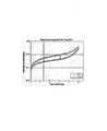
図3及び図4は、本発明に係るNANDフラッシュメモリ素子の漏れ電流を測定したグラフである。 3 and 4 are graphs obtained by measuring the leakage current of the NAND flash memory device according to the present invention.
図3は、テストパターンにおいてセルのしきい電圧が約-5Vの場合、ソース選択ラインをフローティングノードで維持した場合と、0Vに維持した場合の漏れ電流をモニタした結果である。ソース選択ラインとこれと隣接したワードラインの容量性カップリング比(CapacitiveCoupling RatIO)が小さくて誘起されたポテンシャルが0.2ないし0.3V程度にも関わらず、2ないし3倍程度の漏れ電流差を示している。すなわち、ソース選択ラインをフローティングさせた場合より強制的に0Vを印加した場合が漏れ電流が減少することが分かる。 FIG. 3 shows the result of monitoring the leakage current when the threshold voltage of the cell in the test pattern is about −5V and when the source selection line is maintained at the floating node and when it is maintained at 0V. Leakage current difference of about 2 to 3 times even though the capacitive coupling ratio (Capacitive Coupling RatIO) between the source selection line and the adjacent word line is small and the induced potential is about 0.2 to 0.3V. Is shown. That is, it can be seen that the leakage current decreases when 0 V is forcibly applied rather than when the source selection line is floated.
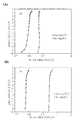
図4Aは、ソース選択ラインを0Vにした場合の漏れ電流をモニタした結果であり、図4Bは、従来1024ブロックの512M製品においてソース選択ラインをフローティングで維持した場合の漏れ電流をモニタした結果である。図4Aないし図4Bに比べて漏れ電流が減少することはもちろん、漏れ電流が均一であることがわかる。すなわち、図4Aが図4Bに比べて約1/4水準に漏れ電流が減少した。 FIG. 4A shows the result of monitoring the leakage current when the source selection line is set to 0V, and FIG. 4B shows the result of monitoring the leakage current when the source selection line is kept floating in a conventional 1024 block 512M product. is there. It can be seen that the leak current is uniform as well as the leak current is reduced as compared with FIGS. That is, FIG. 4A has a leakage current reduced to about 1/4 level compared to FIG. 4B.
尚、本発明は、上記した本実施の形態に限られるものではなく、本発明の技術的思想から逸脱しない範囲内で多様に変更して実施することが可能である。 It should be noted that the present invention is not limited to the above-described embodiment, and can be implemented with various modifications without departing from the technical idea of the present invention.
100 セルブロック
110 セルストリング部
120 ストリング選択部
130 ソース選択部
200 Xデコーダ部
210 ストリング伝送トランジスタ
220 ワードライン伝送トランジスタ
230 ソース伝送トランジスタ
300 スイッチ部
310 ストリング放電トランジスタ
320 ソース放電トランジスタ
DESCRIPTION OF SYMBOLS 100 Cell block 110 Cell string part 120 String selection part 130 Source selection part 200 X decoder part 210 String transmission transistor 220 Word line transmission transistor 230 Source transmission transistor 300 Switch part 310 String discharge transistor 320 Source discharge transistor
Claims (12)
動作信号によってグローバルストリング選択信号、グローバルソース選択信号及び複数のグローバルワードライン信号をそれぞれ前記ローカルストリング選択信号、前記ローカルソース選択信号及び前記複数のローカルワードライン信号に伝送するXデコーダ部と、
所定の制御信号によって前記ローカルストリング選択信号及び前記ローカルソース選択信号に接地電源信号を印加するスイッチ部と
を備えることを特徴とするNANDフラッシュメモリ素子。 A string selection unit that transmits a plurality of bit line signals by a local string selection signal, a source selection unit that transmits a common source line signal by a local source selection signal, a plurality of bit line signals, a common source line signal, and a plurality of local words A cell block including a cell string portion for storing predetermined data by a line signal;
An X decoder for transmitting a global string selection signal, a global source selection signal, and a plurality of global word line signals to the local string selection signal, the local source selection signal, and the plurality of local word line signals, respectively, according to an operation signal;
A NAND flash memory device, comprising: a switch unit that applies a ground power signal to the local string selection signal and the local source selection signal according to a predetermined control signal.
前記制御信号によってそれぞれ前記ローカルストリング選択信号に接地電源を伝送するストリング放電トランジスタと、
前記ローカルソース選択信号に接地電源を伝送するソース放電トランジスタと
を備えることを特徴とする請求項1に記載のNANDフラッシュメモリ素子。 The switch part is
A string discharge transistor for transmitting a ground power to the local string selection signal according to the control signal;
The NAND flash memory device according to claim 1, further comprising: a source discharge transistor that transmits ground power to the local source selection signal.
複数のビットラインにそれぞれ接続され前記ローカルストリング選択信号によって前記ビットライン信号を伝送する複数のストリング選択トランジスタと、
共通ソースラインに接続され前記ローカルソース選択信号によって前記共通ソースライン信号を伝送する複数のソース選択トランジスタと、
直列接続された複数のセルが前記複数のストリング選択トランジスタと前記複数のソース選択トランジスタとの間にそれぞれ接続された複数のセルストリングを含み、複数のセルストリング内の同一位置にある前記セルのゲート各々にローカルワードラインが接続され前記複数のビットライン信号、前記共通ソースライン信号及び前記複数のローカルワードライン信号によって所定のデータを格納したり消去することを特徴とする請求項1に記載のNANDフラッシュメモリ素子。 The cell block is
A plurality of string selection transistors respectively connected to a plurality of bit lines and transmitting the bit line signal by the local string selection signal;
A plurality of source selection transistors connected to a common source line and transmitting the common source line signal by the local source selection signal;
A plurality of cells connected in series include a plurality of cell strings respectively connected between the plurality of string selection transistors and the plurality of source selection transistors, and gates of the cells at the same position in the plurality of cell strings 2. The NAND according to claim 1, wherein a local word line is connected to each of the plurality of bit line signals, the common source line signal, and the plurality of local word line signals to store or erase predetermined data. Flash memory device.
前記動作信号によってそれぞれ前記グローバルストリング選択信号を前記ローカルストリング選択信号に伝送するストリング伝送トランジスタと、
前記グローバルソース選択信号を前記ローカルソース選択信号に伝送するソース伝送トランジスタと、
前記複数のグローバルワードライン信号を前記複数のローカルワードライン信号に伝送する複数のワードライン伝送トランジスタと
を備えることを特徴とする請求項1に記載のNANDフラッシュメモリ素子。 The X decoder unit
A string transmission transistor for transmitting the global string selection signal to the local string selection signal, respectively, according to the operation signal;
A source transmission transistor for transmitting the global source selection signal to the local source selection signal;
The NAND flash memory device of claim 1, further comprising: a plurality of word line transmission transistors that transmit the plurality of global word line signals to the plurality of local word line signals.
それぞれ動作電圧によって駆動しグローバルストリング選択ラインと前記ローカルストリング選択ラインとに接続されたストリング伝送トランジスタと、グローバルソース選択ラインと前記ローカルソース選択ラインとに接続されたソース伝送トランジスタ、複数のグローバルワードラインと前記複数のローカルワードラインとに接続された複数のワードライン伝送トランジスタとを含むXデコーダ部と、
それぞれ制御電圧によって駆動し接地電源と前記ローカルストリング選択ラインとに接続されたストリング放電トランジスタと、接地電源と前記ローカルソース選択ラインとに接続されたソース放電トランジスタとを含むスイッチ部と、
読み出し動作信号によって前記ビットラインに検出電圧を印加し、前記検出電圧の状態によってセルのプログラム及び消去状態を判断するページバッファ部と
を備えるNANDフラッシュメモリ素子の読み取り方法において、
前記Xデコーダ部にグローバルストリング選択電圧、グローバルソース選択電圧及び選択されない複数のワードラインにはパス電圧を印加し、選択されたワードラインには読み出し電圧を印加し、選択された前記セルブロックと接続された前記Xデコーダ部にロジックハイの動作電圧を印加し、選択されない前記セルブロックと接続された前記Xデコーダ部にロジックローの動作電圧を印加するステップと、
選択された前記セルブロックと接続された前記スイッチ部にロジックローの制御電圧を印加し、選択されない前記セルブロックと接続された前記スイッチ部にロジックハイの制御電圧を印加するステップと、
前記共通ソースラインとバルクとに接地電圧を印加し、前記ページバッファを介して選択された前記ビットラインに検出電圧を印加した後、前記検出電圧の変化をセンシングするステップと
を備えることを特徴とするNANDフラッシュメモリ素子の読み取り方法。 A plurality of cell strings connected in series between a plurality of string selection transistors connected to a plurality of bit lines and a plurality of source selection transistors connected to a common source line, and gate terminals of the plurality of string selection transistors A plurality of local string selection lines connected to each other, a local source selection line connected to gate terminals of the plurality of source selection transistors, and a plurality of local word lines connected to the gate terminals of each cell in the cell string. Cell block of
A string transmission transistor driven by an operating voltage and connected to the global string selection line and the local string selection line, a source transmission transistor connected to the global source selection line and the local source selection line, and a plurality of global word lines And an X decoder unit including a plurality of word line transmission transistors connected to the plurality of local word lines,
A switch unit including a string discharge transistor driven by a control voltage and connected to a ground power source and the local string selection line; and a source discharge transistor connected to a ground power source and the local source selection line;
In a reading method of a NAND flash memory device, comprising: a page buffer unit that applies a detection voltage to the bit line according to a read operation signal and determines a program and erase state of a cell according to the state of the detection voltage;
A global string selection voltage, a global source selection voltage, and a pass voltage are applied to a plurality of unselected word lines to the X decoder unit, and a read voltage is applied to the selected word lines and connected to the selected cell block. Applying a logic high operating voltage to the X decoder unit, and applying a logic low operating voltage to the X decoder unit connected to the unselected cell block;
Applying a logic low control voltage to the switch unit connected to the selected cell block, and applying a logic high control voltage to the switch unit connected to the non-selected cell block;
Sensing a change in the detection voltage after applying a ground voltage to the common source line and the bulk, applying a detection voltage to the bit line selected through the page buffer, and A method for reading a NAND flash memory device.
Applications Claiming Priority (1)
| Application Number | Priority Date | Filing Date | Title |
|---|---|---|---|
| KR1020040022677A KR100559716B1 (en) | 2004-04-01 | 2004-04-01 | NAND flash memory device and reading method thereof |
Publications (1)
| Publication Number | Publication Date |
|---|---|
| JP2005293813A true JP2005293813A (en) | 2005-10-20 |
Family
ID=35034188
Family Applications (1)
| Application Number | Title | Priority Date | Filing Date |
|---|---|---|---|
| JP2004192821A Pending JP2005293813A (en) | 2004-04-01 | 2004-06-30 | Nand flash memory device and method of reading the same |
Country Status (6)
| Country | Link |
|---|---|
| US (1) | US7035143B2 (en) |
| JP (1) | JP2005293813A (en) |
| KR (1) | KR100559716B1 (en) |
| CN (1) | CN1677569B (en) |
| DE (1) | DE102004030931A1 (en) |
| TW (1) | TWI264727B (en) |
Cited By (1)
| Publication number | Priority date | Publication date | Assignee | Title |
|---|---|---|---|---|
| JP2009043394A (en) * | 2007-08-06 | 2009-02-26 | Hynix Semiconductor Inc | Block decoder and semiconductor memory element including the same |
Families Citing this family (46)
| Publication number | Priority date | Publication date | Assignee | Title |
|---|---|---|---|---|
| JP3999900B2 (en) * | 1998-09-10 | 2007-10-31 | 株式会社東芝 | Nonvolatile semiconductor memory |
| KR100671625B1 (en) * | 2004-12-28 | 2007-01-19 | 주식회사 하이닉스반도체 | NAND flash memory device that can change the block size |
| KR100612569B1 (en) * | 2005-03-10 | 2006-08-11 | 주식회사 하이닉스반도체 | Flash memory device having improved pre-programming function and its pre-program operation control method |
| US7499326B2 (en) * | 2006-04-12 | 2009-03-03 | Sandisk Corporation | Apparatus for reducing the impact of program disturb |
| US7684243B2 (en) * | 2006-08-31 | 2010-03-23 | Micron Technology, Inc. | Reducing read failure in a memory device |
| KR100827695B1 (en) * | 2006-11-03 | 2008-05-07 | 삼성전자주식회사 | Nonvolatile Semiconductor Memory Device Using Soft Cells as Indicators |
| KR100811278B1 (en) * | 2006-12-29 | 2008-03-07 | 주식회사 하이닉스반도체 | How to Read NAND Flash Memory Devices Using Self-Boosting |
| US7778086B2 (en) * | 2007-01-25 | 2010-08-17 | Micron Technology, Inc. | Erase operation control sequencing apparatus, systems, and methods |
| US7656740B2 (en) * | 2007-02-05 | 2010-02-02 | Micron Technology, Inc. | Wordline voltage transfer apparatus, systems, and methods |
| KR100865821B1 (en) * | 2007-03-14 | 2008-10-28 | 주식회사 하이닉스반도체 | How to Read Nonvolatile Memory Devices |
| JP5057850B2 (en) * | 2007-06-04 | 2012-10-24 | 東芝メモリシステムズ株式会社 | Semiconductor device |
| KR101411976B1 (en) | 2007-07-09 | 2014-06-27 | 삼성전자주식회사 | Flash memory system and its error correction method |
| KR100976694B1 (en) * | 2007-07-25 | 2010-08-18 | 주식회사 하이닉스반도체 | Block Decoder in Nonvolatile Memory Devices |
| US7701761B2 (en) * | 2007-12-20 | 2010-04-20 | Sandisk Corporation | Read, verify word line reference voltage to track source level |
| JP2009206492A (en) * | 2008-01-31 | 2009-09-10 | Toshiba Corp | Semiconductor device |
| KR101458792B1 (en) | 2008-02-11 | 2014-11-10 | 삼성전자주식회사 | Flash memory device |
| KR100965066B1 (en) * | 2008-03-28 | 2010-06-21 | 주식회사 하이닉스반도체 | Flash memory device and its block selection circuit |
| KR101411499B1 (en) | 2008-05-19 | 2014-07-01 | 삼성전자주식회사 | Variable resistance memory device and management method thereof |
| US7889572B2 (en) * | 2008-09-04 | 2011-02-15 | Macronix International Co., Ltd. | Memory with high reading performance and reading method thereof |
| US8164134B2 (en) | 2009-06-09 | 2012-04-24 | Samsung Electronics Co., Ltd. | Semiconductor device |
| JP2011040706A (en) * | 2009-07-15 | 2011-02-24 | Toshiba Corp | Nonvolatile semiconductor memory device |
| US8837221B2 (en) * | 2010-09-03 | 2014-09-16 | Aplus Flash Technology, Inc. | Write bias condition for 2T-string NOR flash cell |
| WO2012084751A1 (en) * | 2010-12-23 | 2012-06-28 | Imec | Vertical memory devices |
| US8614918B2 (en) | 2011-05-02 | 2013-12-24 | Micron Technology, Inc. | Memory apparatus and methods |
| JP2014063556A (en) | 2012-09-24 | 2014-04-10 | Toshiba Corp | Nonvolatile semiconductor memory device |
| KR102127416B1 (en) | 2013-06-27 | 2020-06-26 | 삼성전자주식회사 | Nonvolatile memory device, memory system having the same, and reading method thereof |
| KR102210520B1 (en) * | 2013-12-19 | 2021-02-02 | 삼성전자주식회사 | Nonvolatile memory device and erase method |
| CN104835528B (en) * | 2014-02-07 | 2018-09-11 | 华邦电子股份有限公司 | Flash memory device and data reading method thereof |
| KR20160008875A (en) * | 2014-07-15 | 2016-01-25 | 에스케이하이닉스 주식회사 | Semiconductor memory device and operating method thereof |
| KR20160094117A (en) * | 2015-01-30 | 2016-08-09 | 에스케이하이닉스 주식회사 | Flash memory device |
| KR102424371B1 (en) * | 2016-01-19 | 2022-07-25 | 에스케이하이닉스 주식회사 | Semiconductor memory device and operating method thereof |
| KR102650333B1 (en) | 2016-08-10 | 2024-03-25 | 삼성전자주식회사 | Nonvolatile memory device and storage device including nonvolatile memory device |
| TWI611409B (en) * | 2016-12-08 | 2018-01-11 | 旺宏電子股份有限公司 | Memory device and control method thereof |
| CN108206039B (en) * | 2016-12-19 | 2020-09-11 | 旺宏电子股份有限公司 | Memory device and related control method thereof |
| CN107507639B (en) * | 2017-07-17 | 2020-06-09 | 上海华虹宏力半导体制造有限公司 | Circuit and method for eliminating influence of word line coupling on read margin of SONOS (silicon oxide nitride oxide semiconductor) device |
| US10475510B2 (en) * | 2017-12-21 | 2019-11-12 | Macronix International Co., Ltd. | Leakage compensation read method for memory device |
| JPWO2019181465A1 (en) | 2018-03-19 | 2021-04-30 | 日鉄ケミカル&マテリアル株式会社 | Organic electroluminescent device |
| CN108511021B (en) * | 2018-03-26 | 2020-10-27 | 上海华虹宏力半导体制造有限公司 | Virtual ground flash memory reading circuit |
| US10714166B2 (en) * | 2018-08-13 | 2020-07-14 | Micron Technology, Inc. | Apparatus and methods for decoding memory access addresses for access operations |
| KR102564605B1 (en) * | 2018-12-21 | 2023-08-14 | 에스케이하이닉스 주식회사 | Semiconductor device and manufacturing method of a semiconductor device |
| KR102791813B1 (en) * | 2019-05-16 | 2025-04-08 | 에스케이하이닉스 주식회사 | Memory device, memory system including the memory device and operating method of the memory system |
| CN112309476B (en) * | 2019-07-26 | 2023-03-10 | 西安格易安创集成电路有限公司 | Method and device for reading NAND Flash unit data |
| CN112002357B (en) * | 2020-08-13 | 2023-09-26 | 长江存储科技有限责任公司 | Methods for operating semiconductor devices and semiconductor devices |
| US11756594B2 (en) * | 2020-12-16 | 2023-09-12 | Micron Technology, Inc. | Memory devices for multiple read operations |
| KR102834828B1 (en) * | 2022-02-18 | 2025-07-15 | 양쯔 메모리 테크놀로지스 씨오., 엘티디. | Discharge circuit of AND flash memory |
| US12543325B2 (en) | 2023-04-26 | 2026-02-03 | Macronix International Co., Ltd. | Three-dimensional semiconductor devices |
Family Cites Families (8)
| Publication number | Priority date | Publication date | Assignee | Title |
|---|---|---|---|---|
| JP3890647B2 (en) * | 1997-01-31 | 2007-03-07 | ソニー株式会社 | Nonvolatile semiconductor memory device |
| US5886923A (en) * | 1997-10-27 | 1999-03-23 | Integrated Silicon Solution Inc. | Local row decoder for sector-erase fowler-nordheim tunneling based flash memory |
| KR100301932B1 (en) * | 1999-04-27 | 2001-10-29 | 윤종용 | A non-volatile semiconductor memory device |
| KR100418521B1 (en) * | 2001-06-11 | 2004-02-11 | 삼성전자주식회사 | non-volatile semiconductor memory devices having hierarchical sector structure |
| KR100432884B1 (en) * | 2001-08-28 | 2004-05-22 | 삼성전자주식회사 | Non-volatile semiconductor memory device with shared row selecting circuit |
| KR100463199B1 (en) * | 2002-03-04 | 2004-12-23 | 삼성전자주식회사 | Semiconductor memory device with flexible redundancy scheme |
| KR100502412B1 (en) * | 2002-10-23 | 2005-07-19 | 삼성전자주식회사 | Non-volatile semiconductor memory device and program method thereof |
| KR100559714B1 (en) * | 2004-04-19 | 2006-03-10 | 주식회사 하이닉스반도체 | NAND flash memory device and its programming method |
-
2004
- 2004-04-01 KR KR1020040022677A patent/KR100559716B1/en not_active Expired - Fee Related
- 2004-06-24 US US10/876,319 patent/US7035143B2/en not_active Expired - Lifetime
- 2004-06-25 DE DE102004030931A patent/DE102004030931A1/en not_active Withdrawn
- 2004-06-30 JP JP2004192821A patent/JP2005293813A/en active Pending
- 2004-06-30 TW TW093119305A patent/TWI264727B/en not_active IP Right Cessation
- 2004-08-30 CN CN2004100748926A patent/CN1677569B/en not_active Expired - Lifetime
Cited By (1)
| Publication number | Priority date | Publication date | Assignee | Title |
|---|---|---|---|---|
| JP2009043394A (en) * | 2007-08-06 | 2009-02-26 | Hynix Semiconductor Inc | Block decoder and semiconductor memory element including the same |
Also Published As
| Publication number | Publication date |
|---|---|
| KR100559716B1 (en) | 2006-03-10 |
| CN1677569A (en) | 2005-10-05 |
| US20050226048A1 (en) | 2005-10-13 |
| TW200534287A (en) | 2005-10-16 |
| US7035143B2 (en) | 2006-04-25 |
| KR20050097595A (en) | 2005-10-10 |
| TWI264727B (en) | 2006-10-21 |
| DE102004030931A1 (en) | 2005-10-20 |
| CN1677569B (en) | 2011-05-11 |
Similar Documents
| Publication | Publication Date | Title |
|---|---|---|
| JP2005293813A (en) | Nand flash memory device and method of reading the same | |
| US7161842B2 (en) | Flash memory device and method of erasing flash memory cell thereof | |
| KR100542701B1 (en) | Threshold Voltage Measurement Method for NAND Flash Memory Devices | |
| US7414895B2 (en) | NAND flash memory cell programming | |
| KR100515060B1 (en) | Nonvolatile semiconductor memory device having constant bit line precharge level | |
| US6285587B1 (en) | Memory cell string structure of a flash memory device | |
| US8320184B2 (en) | Method of programming nonvolatile semiconductor memory device | |
| JP2005310347A (en) | Nand flash memory device and method of programming the same | |
| KR20040015897A (en) | Flash memory array having source line free from bitline coupling and loading effect | |
| JP4698605B2 (en) | Semiconductor device and method for controlling semiconductor device | |
| KR20160051530A (en) | Nand type flash memory and programming method thereof | |
| KR20090026502A (en) | How flash memory devices work | |
| KR20090075535A (en) | Program Verification Method of Flash Memory Device Obtaining Wide Pass Voltage Window | |
| JP2001093287A (en) | Nonvolatile semiconductor memory device | |
| KR20100022228A (en) | Non volatile memory device and method of operating the same | |
| KR100855962B1 (en) | Read method of nonvolatile memory device and nonvolatile memory device | |
| KR20120037187A (en) | Semiconductor memory device and method for operating thereof | |
| KR20120069115A (en) | Semiconductor memory device and method for operating thereof | |
| KR100634456B1 (en) | Flash memory device and its reading method | |
| KR20040085616A (en) | Semiconductor memory device | |
| KR102064514B1 (en) | Method for operating semiconductor memory device | |
| KR100908540B1 (en) | Nand flash memory device | |
| KR20120005850A (en) | How Nonvolatile Memory Devices Work | |
| KR20120078839A (en) | Semiconductor memory device and erase method thereof | |
| KR20070021370A (en) | Program method of flash memory device |
Legal Events
| Date | Code | Title | Description |
|---|---|---|---|
| A621 | Written request for application examination |
Free format text: JAPANESE INTERMEDIATE CODE: A621 Effective date: 20060512 |
|
| A977 | Report on retrieval |
Free format text: JAPANESE INTERMEDIATE CODE: A971007 Effective date: 20081224 |
|
| A131 | Notification of reasons for refusal |
Free format text: JAPANESE INTERMEDIATE CODE: A131 Effective date: 20090120 |
|
| A521 | Request for written amendment filed |
Free format text: JAPANESE INTERMEDIATE CODE: A523 Effective date: 20090420 |
|
| A02 | Decision of refusal |
Free format text: JAPANESE INTERMEDIATE CODE: A02 Effective date: 20090908 |