JP2005293060A - Memory card housing and manufacturing method thereof - Google Patents
Memory card housing and manufacturing method thereof Download PDFInfo
- Publication number
- JP2005293060A JP2005293060A JP2004105232A JP2004105232A JP2005293060A JP 2005293060 A JP2005293060 A JP 2005293060A JP 2004105232 A JP2004105232 A JP 2004105232A JP 2004105232 A JP2004105232 A JP 2004105232A JP 2005293060 A JP2005293060 A JP 2005293060A
- Authority
- JP
- Japan
- Prior art keywords
- cover
- memory card
- cover frame
- frame
- mold
- Prior art date
- Legal status (The legal status is an assumption and is not a legal conclusion. Google has not performed a legal analysis and makes no representation as to the accuracy of the status listed.)
- Pending
Links
Images
Landscapes
- Containers Having Bodies Formed In One Piece (AREA)
- Injection Moulding Of Plastics Or The Like (AREA)
Abstract
【課題】構成が簡素で、かつ薄くて損傷に強いメモリーカードの筐体の製造技術の提供。
【解決手段】メモリーカード1の筐体2は、1枚の屈曲可能な薄片シート(薄板材)3に第1カバー4を構成する第1カバー用枠体6と第2カバー5を構成する第2カバー用枠体7を射出成形したものである。2つのカバー用枠体を有するメモリーカード1の筐体2は、2つのカバーを電子回路基板8装入後折り曲げて、2つのカバー用枠体を重ね合わせて一体的に接合される。
【選択図】 図2Provided is a manufacturing technique for a memory card casing which is simple in structure, thin and resistant to damage.
A housing 2 of a memory card 1 has a first cover frame 6 and a second cover 5 constituting a first cover 4 on a single bendable thin sheet (thin plate material) 3. The two-cover frame 7 is injection-molded. The housing 2 of the memory card 1 having two cover frames is joined integrally by overlapping the two covers and bending the two covers after inserting the electronic circuit board 8.
[Selection] Figure 2
Description
本発明は、電子回路基板を内蔵するメモリーカードの筐体の製造技術に関する。更に詳しくは、SDメモリーカード等の小型メモリーカードの筐体とその製造技術に関する。 The present invention relates to a technique for manufacturing a housing of a memory card incorporating an electronic circuit board. More specifically, the present invention relates to a case of a small memory card such as an SD memory card and a manufacturing technique thereof.
従来から、カードタイプのメモリー装置は公知であるが、最近は更に容量が大きく小型のメモリーカードが要求され開発されている。例えばSDメモリーカードは、内部に電子回路基板を内蔵し切手型ともいわれ極めて薄い扁平上のメモリーカードで、デジタルカメラや音楽機器等の分野で広く使用されている。一般にこのメモリーカードの筐体部分は、内部に電子回路基板を装入してから分割された2つのカバーを相対接合しメモリーカードのケースとして作成される。 Conventionally, card-type memory devices are known, but recently, a memory card having a larger capacity and a smaller size is required and developed. For example, an SD memory card is an extremely thin flat memory card that is also called a stamp type and has an electronic circuit board inside, and is widely used in the fields of digital cameras and music equipment. In general, the housing portion of the memory card is formed as a memory card case by relatively joining two covers that are divided after an electronic circuit board is inserted therein.
このメモリーカードは薄く扁平状のものである。内蔵された電子回路基板には、外部電子機器との接触のためコンタクト部が設けられている。このコンタクト部は、切り欠き状に設けられた筐体の窓を通して外部機器と接触する。筐体の窓は、コンタクト部をカード外部に対向させるため、コンタクト部と外部とを貫通した筐体の穴である。 This memory card is thin and flat. The built-in electronic circuit board is provided with a contact portion for contact with an external electronic device. This contact portion comes into contact with an external device through a window of a casing provided in a cutout shape. The window of the housing is a hole in the housing that penetrates the contact portion and the outside in order to make the contact portion face the outside of the card.
従って、メモリーカードの情報はコンタクト部が外部の電子機器と直接接触することにより電気的に接続され伝達される。筐体を構成する2つのカバーは、従来から独立して個々に成形して設けられた成形品である。この2つのカバーを位置合わせして超音波溶着等で固定してメモリーカードとする。このような構成のメモリーカードは例えば特許文献1に示されるように、独立した2つのカバーを単に突合せ固定しているものである。又、2つのカバーは、それぞれ全体が射出成形された成形品である。又、メモリーカードの製造方法については、そのカバーを成形して製造されるが、例えば、特許文献2に示されるように、カバーの肉厚が薄いことに伴い、金型による射出成形の際、ガスを抜くようにしてキャビティに合成樹脂を射出する方法が開示されている。このように、従来のメモリーカードの筐体は、個々に成形により製造されたカバーを重ね合わせてケースにする構成のものである。
前述のように、従来のメモリーカードの筐体は個別に設けられた2つのカバー構成のものである。個々のカバーについては全てを射出成形した成形品である。しかし、全てを成形品で構成すると、薄くするためには限界があり、成形での安定した製造を行なう上では、どうしてもある程度厚くならざるを得ないのが現状である。近年の流れとして全ての電子機器は小型化にありしかも大容量であることが望まれている。 As described above, the housing of the conventional memory card has two cover configurations provided separately. The individual covers are all molded products obtained by injection molding. However, if all are formed of molded products, there is a limit to reducing the thickness, and the current situation is that the thickness must be increased to some extent in order to achieve stable manufacturing by molding. In recent years, it is desired that all electronic devices are downsized and have a large capacity.
この小型電子装置の一つであるメモリーカードは、フラッシュメモリーと呼ばれるROMを組み込んだもので、通称切手型ともいわれる小型形状の記憶装置である。このメモリーカードは、現状例えば、SD(Secure Digital)メモリーカード、メモリースティック(ソニー開発製品)、スマートメディア(東芝開発製品)等が市販されている。デジタルカメラの記憶媒体や音響機器の記憶媒体として利用されている。近年大容量化の方向に開発努力がなされている。 A memory card, which is one of the small electronic devices, incorporates a ROM called a flash memory, and is a small-sized storage device called a so-called stamp type. Currently, for example, SD (Secure Digital) memory cards, memory sticks (developed by Sony), smart media (developed by Toshiba), etc. are commercially available. It is used as a storage medium for digital cameras and a storage medium for audio equipment. In recent years, development efforts have been made in the direction of increasing capacity.
例えば、SDメモリーカードは、更に薄くすることが要求されている。SDカードの場合は、カードそのものの厚さが規定されている。従って、規定厚さ内にメモリーカードを作成しなければならない。従来の成形されたカバーによるケース構成のメモリーカードであると、成形のための面厚さが必要であり、このため内蔵される電子部品の厚さが相対的に薄くせざるを得ない問題点がある。電子部品の厚さに制約があると、メモリー容量が制限されることになる。又、2つのカバーを個別に製造し、このカバーを位置合わせして接合することになるので、製造上のコストアップになり、それなりにコストを要する製造方法である。 For example, an SD memory card is required to be thinner. In the case of an SD card, the thickness of the card itself is specified. Therefore, the memory card must be created within the specified thickness. A memory card with a case structure using a conventional molded cover requires a surface thickness for molding, and the thickness of the built-in electronic components must be relatively thin. There is. If the thickness of the electronic component is limited, the memory capacity is limited. Further, since the two covers are individually manufactured, and the covers are aligned and joined, the manufacturing cost is increased, and the manufacturing method requires a certain amount of cost.
又、前述の特許文献2に示される技術は、特にオーディオ装置に使用されるメモリーカードを対象にしていて、肉厚の薄いカバー張り合わせ構成のカードケースを射出成形する技術として開示されている。しかし、残留応力を除くようなことを考慮しなければならず、ガス抜きのために金型にガス抜き回路を設けるなど金型構成が複雑になっている。大量生産を効果的に行なうにはさらに製造上のコスト低減が求められていた。
Further, the technique disclosed in
本発明は、このような技術的背景に基づいてなされたものであり、下記の目的を達成するものである。
本発明の目的は、メモリーカードの筐体の面厚さをシート構成で薄くし、成形に伴う残留応力のない筐体の製造技術を提供することにある。本発明の他の目的は、メモリーカードを低コストで製造できる筐体の製造技術を提供することにある。
The present invention has been made based on such a technical background, and achieves the following objects.
SUMMARY OF THE INVENTION An object of the present invention is to provide a manufacturing technique of a housing that is free from residual stress associated with molding by reducing the surface thickness of the housing of the memory card by a sheet configuration. Another object of the present invention is to provide a manufacturing technique for a housing that can manufacture a memory card at low cost.
前記課題を解決するために次のような手段を採る。
本発明1のメモリーカードの筐体は、所定形状に切断された屈曲可能な薄片シートと、金型にインサートされる前記薄片シートの所定位置に射出成形され、第1カバーを形成する合成樹脂の第1カバー用枠体と、前記薄片シートの所定位置に射出成形され、第2カバーを形成する合成樹脂の第2カバー用枠体とからなり、
前記第1カバー用枠体及び前記第2カバー用枠体が射出成形された後、前記第1カバー内に電子回路基板を装入してから、前記第2カバーを前記第1カバーとの間で折り曲げ前記2つのカバー用枠体の重ね合わせが可能になることを特徴とする。
折り曲げ部分は、屈曲可能な薄片シートであるので、第1カバー用枠体と第2カバー用枠体はこの1つの薄片シートにより容易に折り曲げることができ、枠体を成形した後に電子部品を内蔵し重ね合わせるだけでメモリーカードが容易にできる。又、メモリーカードのカバー面を薄くしているので、相対的に内臓する電子回路基板の部品を厚くすることができメモリーの容量を大きくすることが可能である。
In order to solve the above problems, the following means are adopted.
The case of the memory card according to the first aspect of the present invention includes a bendable thin sheet cut into a predetermined shape and a synthetic resin that is injection-molded at a predetermined position of the thin sheet inserted into a mold to form a first cover. A first cover frame and a synthetic resin second cover frame that is injection-molded at a predetermined position of the thin sheet and forms a second cover;
After the first cover frame and the second cover frame are injection-molded, an electronic circuit board is inserted into the first cover, and then the second cover is placed between the first cover and the first cover. The two cover frames can be overlapped by bending at a point.
Since the folded portion is a bendable thin sheet, the first cover frame and the second cover frame can be easily folded by this one thin sheet, and the electronic parts are built in after the frame is formed. Then, memory cards can be easily created simply by overlapping them. In addition, since the cover surface of the memory card is made thin, it is possible to make the components of the electronic circuit board that is relatively built-in relatively thick and to increase the memory capacity.
本発明2のメモリーカードの筐体は、本発明1において、前記薄片シートは合成樹脂のシートであることを特徴とする。市販の合成樹脂のシートの使用が可能であり、シート面が均一で丈夫である。
The housing of the memory card of the
本発明3のメモリーカードの筐体は、本発明1において、前記第1カバー用枠体及び前記第2カバー用枠体の重ね合わせ部分は、相互に嵌め合いの可能な段差部又は凹凸部が設けられていることを特徴とする。段差部又は凹凸部は位置合わせを正確に、重ね合わせを確実に行なう点で有効である。 The housing of the memory card according to the third aspect of the present invention is the first aspect of the present invention, wherein the overlapping portion of the first cover frame and the second cover frame has a stepped portion or an uneven portion that can be fitted to each other. It is provided. The stepped portion or the uneven portion is effective in that the alignment is performed accurately and the overlapping is performed with certainty.
本発明4のメモリーカードの筐体は、本発明1において、前記第1カバー用枠体又は前記第2カバー用枠体に表裏貫通する窓穴が設けられていることを特徴とする。電子回路基板のコンタクト部が外部の電子機器と直接接触できる構成となる。
The housing of the memory card of the
本発明5のメモリーカードの筐体は、本発明1および2において、前記第1カバー用枠体及び前記第2カバー用枠体は前記薄片シートの周縁部に設けられていることを特徴とする。前記第1カバー用枠体及び前記第2カバー用枠体の内部に囲まれる状態で電子回路基板を内蔵することができる。 The housing of the memory card according to the fifth aspect of the present invention is characterized in that, in the first and second aspects of the present invention, the first cover frame and the second cover frame are provided on a peripheral portion of the thin sheet. . An electronic circuit board can be built in a state surrounded by the first cover frame and the second cover frame.
本発明6のメモリーカードの筐体の製造方法は、屈曲する薄片シートを所定形状に切断する工程と、切断された前記薄片シートを第1金型にインサートする工程と、前記薄片シートに第1カバーのための第1カバー用枠体と第2カバーのための第2カバー用枠体を形成するため前記第1金型に相対して第2金型を進退させ、金型内にキャビティを形成する工程と、前記第1金型と前記第2金型が閉じたときゲートを介し前記第1カバー用枠体及び前記第2カバー用枠体のキャビティに合成樹脂を射出する工程とからなり、前記第1カバー用枠体及び前記第2カバー用枠体の射出成形工程後前記第1カバー内に電子回路基板を装入してから、前記第2カバーを前記第1カバーとの間で折り曲げ前記2つのカバー用枠体の重ね合わせを可能とすることを特徴とする。 The method of manufacturing a memory card casing according to the sixth aspect of the present invention includes a step of cutting a bent thin sheet into a predetermined shape, a step of inserting the cut thin sheet into a first mold, and a first step on the thin sheet. A second mold is advanced and retracted relative to the first mold to form a first cover frame for the cover and a second cover frame for the second cover, and a cavity is formed in the mold. And a step of injecting synthetic resin into the cavities of the first cover frame and the second cover frame through a gate when the first mold and the second mold are closed. The electronic circuit board is inserted into the first cover after the injection molding process of the first cover frame and the second cover frame, and then the second cover is placed between the first cover and the first cover. Bending enables the two cover frames to be overlapped And wherein the door.
本発明のメモリーカードの筐体の面厚さをシート構成で薄くすることができたので、筐体は成形に伴う残留応力はなく、しかも筐体の面厚さを薄くしたことに相対して電子回路基板の部品厚さを厚くすることができる。この結果、メモリーカードのメモリー容量を大きくすることが可能となった。又、成形構成を簡素にすることができたので、メモリーカードを低コストで製造できることとなった。 Since the surface thickness of the case of the memory card of the present invention can be reduced by the sheet configuration, the case has no residual stress accompanying molding, and in contrast to the reduction in the case thickness. The component thickness of the electronic circuit board can be increased. As a result, the memory capacity of the memory card can be increased. Further, since the molding configuration can be simplified, the memory card can be manufactured at a low cost.
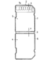
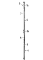
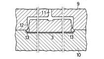
以下、図をもとに本発明の実施の形態を説明する。図1は、本発明の成形直後のメモリーカード1の筐体2を示す平面図である。図2は成形直後のメモリーカード1の筐体2を示す断面図である。図3及び図4は、薄片シートである薄板材3に第1カバー4の第1カバー用枠体6(以下枠体とも略称する)又は第2カバー5の第2カバー用枠体7(以下枠体とも略称する)を射出成形する金型構成の部分断面図である。図5は、射出成形された筐体2を折り曲げる過程の説明図である。図6は、電子回路基板8のコンタクト部8aの部位のメモリーカード1の部分断面図である。図7は、電子回路基板8が内臓されたメモリーカード1の部分断面図で、筐体2の折り曲げ部分の構成を示す。図8から図10は筐体2とメモリーカード1の製造方法に関わる断面図である。
Hereinafter, embodiments of the present invention will be described with reference to the drawings. FIG. 1 is a plan view showing a
次にこれらの図をもとに本発明を詳細に説明する。基本的に筐体2は薄板材3に第1カバー用枠体6が形成された第1カバー4と、前記同一の薄板材3に第2カバー用枠体7が形成された第2カバー5とから構成されている。メモリーカード1は、この第1カバー4と第2カバー5で電子回路基板8を挟持して重ね合わせて固定されたものである。扁平状のもので極めて薄い形状をなす。
Next, the present invention will be described in detail with reference to these drawings. Basically, the
図3及び図4は薄板材3に枠体を成形する構成を示した部分断面図であるが、第1カバー用枠体6又は第2カバー用枠体7の一方を示したものである。他方は相対して段差部6a(7b)の形状は異なる。即ち、この段差部6a(7b)は、一方が高い部分に対して他方は低く、逆に一方が低い部分に対して他方は高くして、重ね合わせたとき枠体の合わせ面が一致するようにしている。成形形態は第1カバー用枠体、第2カバー用枠体ともどちらも同じである。
FIGS. 3 and 4 are partial cross-sectional views showing a configuration in which a frame body is formed on the
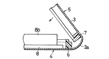
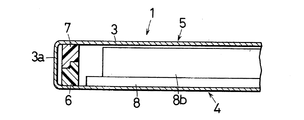
図6及び図7は、電子回路基板8を2つのカバー用枠体6,7を有する2つのカバー4,5で挟持して構成されたメモリーカード1の断面図を示しているが、本発明の理解を容易にするためこの図をもとにメモリーカード1の構成について説明する。図6は、図1に示す筐体2のX位置に相当する部分のメモリーカード1の部分断面図である。
6 and 7 show cross-sectional views of the memory card 1 configured by sandwiching the
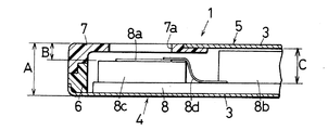
図7は図1に示す筐体2のY位置に相当する部分のメモリーカード1の部分断面図である。前述のように、メモリーカード1は、2つのカバー4,5で電子回路基板8を挟み込んだ構成のものであるが、全体の厚みAが規制されている。又、メモリーカード1の外表面と電子回路基板8のコンタクト部8aとの間隔Bも所定寸法に定められている。電子回路基板8に取り付けられる電子回路部品8bの許容厚さはCとなる。この条件の範囲以内にメモリーカード1を構成しなければならない。
FIG. 7 is a partial cross-sectional view of the memory card 1 corresponding to the Y position of the
メモリーカード1のカバーの厚みを薄くすれば、内臓される電子回路部品8bの厚さに余裕が生じることになり、従来より厚い電子回路部品8bの取り付けが可能となる。このことは従来より容量の大きい電子回路部品8bの設置が可能であることを意味する。メモリーカード1の一方の第1カバー4に電子回路基板8が取り付けられていて、この電子回路基板8に電子回路部品8bとコンタクト部基板8c等の部品が設けられている。コンタクト部8aと電子回路部品8bとの間には、この両者を電気的に導電させる導電部材8dが接続されている。
If the thickness of the cover of the memory card 1 is reduced, there will be a margin in the thickness of the built-in
他方の第2カバー5には個々のコンタクト部8aに対向して複数の開口部が設けられている。この開口部はコンタクト部8aと互いに対向する形態をとっているコンタクト窓7aである。このコンタクト窓7a部分は、第2カバー用枠体7の一部となっている。コンタクト部8aは、外部電子機器との接続端子である。第2カバー7はカバー面部分が電子回路部品8bに対向していて、通常はスペースの許容する範囲で最大寸法(図7のCに近い寸法)の電子回路部品8bが設置される。
The other
本発明は、このように構成されるメモリーカード1の筐体2とその製造技術にに関わる。図1は内蔵される電子回路部品8b側からみた場合の筐体2の平面図である。この筐体2のカバー面は薄片シートである薄板材3で構成されている。この薄板材3の周縁部に第1カバー用枠体6と第2カバー用枠体7の2つの枠体が射出成形により成形され、それぞれ第1カバー4と第2カバー5を構成する。第2カバー5にコンタクト窓7aが設けられている。次にこの筐体2の製造技術について説明する。
The present invention relates to the
従来は前述のように筐体全体が合成樹脂製の成形品であった。この合成樹脂製の成形品は、射出成形によって複雑な形状のものができるが、カバー面を薄くするには限界がある。これに比し本発明の筐体2は、カバー面部に相当する部分を薄板材3とするものである。本実施の形態においては、合成樹脂製のフィルム状(薄膜)の薄板材3を使用し、その外周縁部に合成樹脂を射出し枠体を成形し、この枠体は第1カバー用枠体6と第カバー用枠体7から構成される。この枠体は基本的に薄板材3の外周縁部に成形するので、カバーに残留応力が生じ、カバーが変形することはない。薄板材3はPBT(ポリブチレンテレフタレート),ABS樹脂、PC(ポリカーボネート),PET(ポリエチレンテレフタレート)等であり、損傷等に強い合成樹脂である。
Conventionally, as described above, the entire casing is a molded product made of synthetic resin. This synthetic resin molded product can be made into a complicated shape by injection molding, but there is a limit to making the cover surface thinner. On the other hand, the
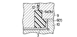
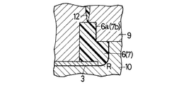
本実施の形態では、板厚の寸法が0.1mm以下のものの使用が可能である。この成形構成を示したのが図8及び図9である。この図は枠体が射出成形される前の状態を示している。この形態では、予め所定寸法に切断された薄板材3を射出成形金型の固定金型9に公知の真空吸着等の手段(図示せず)で吸着させ配置する。この後、可動金型10を固定金型9に移動させて薄板材3を加圧(プレス)して図9に示すように、薄板材3を可動金型10の金型形状に沿って角部がR形状になるように変形させる。プレス成形方法についての技術は公知であるので、詳細説明は省略する。
In the present embodiment, it is possible to use a plate having a thickness of 0.1 mm or less. FIG. 8 and FIG. 9 show this molding configuration. This figure shows a state before the frame is injection molded. In this embodiment, the
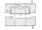
枠体を形成するために、射出成形機のノズル先端からスプールに溶融樹脂が射出され(図示せず)、ランナー11、ゲート12を通って、枠体を構成する金型のキャビティ13に合成樹脂が充填される。この充填によって、薄板材3は金型形状に沿って密着した状態となり、薄板材3と枠体が一体となった筐体2が成形される。もし薄板材3が枠体の一体部分からはみ出たら、そのはみ出た薄板材3は後で除去すればよい。
In order to form a frame body, molten resin is injected from a nozzle tip of an injection molding machine onto a spool (not shown), passes through a
図9の形態は、筐体2の完成品に近い形状に予めトリミングした薄板材3を可動金型10にプレスでインサートした後、この薄板材3に枠体を成形する状態を示している。薄板材3の周縁部は金型の枠体のキャビティ13内のR部で若干まくれ上がる形状になっている。しかし、薄板材3と枠体の関係は、図4に示すように薄板材3の端部が金型のR部に達せず、カバーのR部は枠体の一部として滑らかに射出成形される。又、図5に示す構成は、薄板材3が枠体側に張出しカバーのR部は薄板材3の端部で構成し枠体と一体化され滑らかに成形される。この場合は前述のように、薄板材3の切断部にバリも発生するが、射出成形のとき枠体と共に金型形状に沿って溶融して一体化する。
The form of FIG. 9 shows a state in which a
この実施の形態の場合は、筐体完成後に枠体周縁部に張出した薄板材3を除去するための仕上は必要ない。このように熱融着させる合成樹脂は、薄板材3と枠体が同一の樹脂材料であることが好ましい。熱融着がスムースに行なえる。このような射出成形は、生産性向上の観点から複数の製品に対して同時に行なうので、実際は複数のキャビティ13に1つのランナー11から溶融された合成樹脂が射出されることになる。
In the case of this embodiment, it is not necessary to finish to remove the
枠体は図に示すように、接合部が段差部6a,7b、即ち、第1カバー用枠体6の段差部6a、第2カバー用枠体7の段差部7bとして構成されている。この段差部6a,7bが相手カバー用枠体と相互に接合し重ね合わせられ一体化する。段差部6a,7bを構成したことによりこの接合部は、接合強度が高められ、又位置合わせも容易になる。筐体2はこのようにして成形されるが、前述したようにこの筐体2は2つのカバー用枠体6,7が個別に1つの薄板材3に設けられた構成である。筐体2としては以上の工程で完成するが、この構成は、メモリーカード1を作る過程において、次の工程を施す上に有効な形態となっている。即ち、この筐体2は折り曲げ重ね合わせることでメモリーカード1のケースとして完成させることができるのである。
As shown in the figure, the frame is configured such that the joints are stepped
一方の第1カバー用枠体6内に電子回路基板8を装入してから他方の第2カバー用枠体7部分を第1カバー用枠体6との間の折り曲げ薄板材部分3aを中心に矢印の方向に折り曲げる。この折り曲げ過程を示したのが図5である。この折り曲げ薄板材部分3aは屈曲可能であるから自由に折り曲げることができる。生産性を向上させるためには、この折り曲げ工程は、専用の治具を作成し機械的に自動化するのが好ましい。折り曲げられた後は2つのカバーを接着することになるが、これを超音波溶着で行なう。次にこの超音波溶着の方法を説明する。
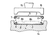
After the
図10は、超音波溶着する場合の断面図である。折り曲げられた一方の第1カバー4をホルダ14(固定治具)の所定位置に位置決めし、他方の第2カバー5を折り曲げ、第1カバー用枠体6と第2カバー用枠体7とを被せ重ね合わせた後、超音波溶着装置の超音波発振器(図示せず)により駆動される固定ホーン15の先端に固定された工具ホーン16が下降し、枠体部分の接合部が加圧される。この加圧のとき接合部は、超音波振動を与えられて摩擦熱で溶着される。図の構成は、理解を容易にするため2つのカバーを離した状態になっているが、実際は重ね合わせた状態で溶着される。
FIG. 10 is a cross-sectional view when ultrasonic welding is performed. One bent
接合される接合部即ち段差部6a,7bには溶着部(リッジ)17が形成されていて、超音波振動は、この溶着部(リッジ)17に与えられ接合を施す。この溶着部(リッジ)17を介して接合することは公知であり、溶着部(リッジ)17を設けたことは接合部を強固にする上で有効である。この超音波溶着は、接合部の仕上がりがきれいで、溶着時間も短いので、能率的な固着方法である。このようにして1枚の薄片シートに形成された2つのカバーが折り曲げ重ね合わされることによってメモリーカードが容易に製造される。
A welded portion (ridge) 17 is formed in the joined portions, that is, the
実施の形態の図は、説明用に模式的に示されているが、実際のメモリーカード1は、極めて薄い製品である。筐体2のカバー部をシートにしたことで従来より一層薄くすることが可能である。このメモリーカード1は、筐体2のカバー部に成形前の薄板材3に予め印刷等も施すことができる。本発明の場合は、枠体のみの成形であり、成形上の簡素化を考慮すると、量産品に伴うコスト削減効果は極めて大きい。
なお、前述した熱成形は、真空成形であるので成形圧が1気圧以下であるが、2〜8気圧程度の圧縮空気を使用して成形する圧空成形(プレッシャ成形)であっても良い。枠体の接合部を2段の段差部としたが、3段以上であってもよい。また凹凸形状であってもよい。又、薄板材に対する射出成形は枠体のみでの説明であったが、カバーを補強するためのリブ状の成形体を内蔵される電子回路部品の形態に合わせ薄板材に設けてもよい。いずれにしろ、本発明は、以上説明した実施の形態に限定されないことはいうまでもない。
Although the drawings of the embodiments are schematically shown for explanation, the actual memory card 1 is a very thin product. By making the cover part of the housing | casing 2 into a sheet | seat, it can be made still thinner than before. The memory card 1 can be printed in advance on the
The above-described thermoforming is vacuum forming, so that the forming pressure is 1 atm or less, but it may be pressure air forming (pressure forming) using 2 to 8 atm of compressed air. Although the joint portion of the frame is a two-step step portion, it may be three or more steps. Further, it may be uneven. Moreover, although the injection molding for the thin plate material has been described only with the frame body, a rib-shaped molded body for reinforcing the cover may be provided on the thin plate material in accordance with the form of the built-in electronic circuit component. In any case, it goes without saying that the present invention is not limited to the embodiment described above.
1…メモリーカード
2…筐体
3…薄板材
4…第1カバー
5…第2カバー
6…第1カバー用枠体
7…第2カバー用枠体
8…電子回路基板
9…固定金型
10…可動金型
DESCRIPTION OF SYMBOLS 1 ...
Claims (6)
金型にインサートされる前記薄片シートの所定位置に射出成形され、第1カバーを形成する合成樹脂の第1カバー用枠体と、
前記薄片シートの所定位置に射出成形され、第2カバーを形成する合成樹脂の第2カバー用枠体とからなり、
前記第1カバー用枠体及び前記第2カバー用枠体が射出成形された後、前記第1カバー内に電子回路基板を装入してから、前記第2カバーを前記第1カバーとの間で折り曲げ前記2つのカバー用枠体の重ね合わせが可能になるメモリーカードの筐体。 A bendable flake sheet cut into a predetermined shape;
A synthetic resin first cover frame that is injection-molded at a predetermined position of the thin sheet inserted into a mold and forms a first cover;
A synthetic resin second cover frame which is injection molded at a predetermined position of the thin sheet and forms a second cover;
After the first cover frame and the second cover frame are injection-molded, an electronic circuit board is inserted into the first cover, and then the second cover is placed between the first cover and the first cover. A memory card housing which can be folded at the two cover frames.
前記薄片シートは合成樹脂のシートであることを特徴とするメモリーカードの筐体。 The memory card housing according to claim 1,
The memory card housing, wherein the thin sheet is a synthetic resin sheet.
前記第1カバー用枠体及び前記第2カバー用枠体の重ね合わせ部分は、相互に嵌め合いの可能な段差部又は凹凸部が設けられていることを特徴とするメモリーカードの筐体。 The memory card housing according to claim 1,
The memory card housing, wherein the overlapping portion of the first cover frame and the second cover frame is provided with a stepped portion or an uneven portion that can be fitted to each other.
前記第1カバー用枠体又は前記第2カバー用枠体に表裏貫通する窓穴が設けられていることを特徴とするメモリーカードの筐体。 The memory card housing according to claim 1,
A housing for a memory card, wherein a window hole penetrating front and back is provided in the first cover frame or the second cover frame.
前記第1カバー用枠体及び前記第2カバー用枠体は前記薄片シートの周縁部に設けられていることを特徴とするメモリーカードの筐体。 The memory card housing according to claim 1,
The memory card housing according to claim 1, wherein the first cover frame and the second cover frame are provided on a peripheral portion of the thin sheet.
切断された前記薄片シートを第1金型にインサートする工程と、
前記薄片シートに第1カバーのための第1カバー用枠体と第2カバーのための第2カバー用枠体を形成するため前記第1金型に相対して第2金型を進退させ、金型内にキャビティを形成する工程と、
前記第1金型と前記第2金型が閉じたときゲートを介し前記第1カバー用枠体及び前記第2カバー用枠体のキャビティに合成樹脂を射出する工程とからなり、
前記第1カバー用枠体及び前記第2カバー用枠体の射出成形工程後前記第1カバー内に電子回路基板を装入してから、前記第2カバーを前記第1カバーとの間で折り曲げ前記2つのカバー用枠体の重ね合わせを可能とするメモリーカードの筐体の製造方法。
Cutting the bent thin sheet into a predetermined shape;
Inserting the cut flake sheet into a first mold;
Advancing and retracting the second mold relative to the first mold to form a first cover frame for the first cover and a second cover frame for the second cover on the thin sheet; Forming a cavity in the mold; and
And a step of injecting synthetic resin into the cavities of the first cover frame and the second cover frame through a gate when the first mold and the second mold are closed,
After an injection molding process of the first cover frame and the second cover frame, an electronic circuit board is inserted into the first cover, and then the second cover is bent between the first cover and the first cover. A method of manufacturing a memory card housing, which enables the two cover frames to be superimposed.
Priority Applications (1)
| Application Number | Priority Date | Filing Date | Title |
|---|---|---|---|
| JP2004105232A JP2005293060A (en) | 2004-03-31 | 2004-03-31 | Memory card housing and manufacturing method thereof |
Applications Claiming Priority (1)
| Application Number | Priority Date | Filing Date | Title |
|---|---|---|---|
| JP2004105232A JP2005293060A (en) | 2004-03-31 | 2004-03-31 | Memory card housing and manufacturing method thereof |
Publications (1)
| Publication Number | Publication Date |
|---|---|
| JP2005293060A true JP2005293060A (en) | 2005-10-20 |
Family
ID=35325944
Family Applications (1)
| Application Number | Title | Priority Date | Filing Date |
|---|---|---|---|
| JP2004105232A Pending JP2005293060A (en) | 2004-03-31 | 2004-03-31 | Memory card housing and manufacturing method thereof |
Country Status (1)
| Country | Link |
|---|---|
| JP (1) | JP2005293060A (en) |
Cited By (3)
| Publication number | Priority date | Publication date | Assignee | Title |
|---|---|---|---|---|
| JP2007172572A (en) * | 2005-12-23 | 2007-07-05 | Chin-Tong Liu | Memory card mounting method and structure |
| KR101402072B1 (en) * | 2012-12-28 | 2014-06-27 | 안봉규 | Method for processing memory disk case |
| JP2018187860A (en) * | 2017-05-09 | 2018-11-29 | カルソニックカンセイ株式会社 | Decorative case manufacturing method and decorative case |
Citations (4)
| Publication number | Priority date | Publication date | Assignee | Title |
|---|---|---|---|---|
| JPS5139458A (en) * | 1974-09-30 | 1976-04-02 | Mitsubishi Electric Corp | Fuirutaa oyobi sonoseizohoho narabini sochi |
| JPH0324721U (en) * | 1989-07-20 | 1991-03-14 | ||
| JP2003303326A (en) * | 2002-04-10 | 2003-10-24 | Murata Mfg Co Ltd | Card type module and method for manufacturing the card type module |
| JP2004038266A (en) * | 2002-06-28 | 2004-02-05 | Toshiba Corp | Card device |
-
2004
- 2004-03-31 JP JP2004105232A patent/JP2005293060A/en active Pending
Patent Citations (4)
| Publication number | Priority date | Publication date | Assignee | Title |
|---|---|---|---|---|
| JPS5139458A (en) * | 1974-09-30 | 1976-04-02 | Mitsubishi Electric Corp | Fuirutaa oyobi sonoseizohoho narabini sochi |
| JPH0324721U (en) * | 1989-07-20 | 1991-03-14 | ||
| JP2003303326A (en) * | 2002-04-10 | 2003-10-24 | Murata Mfg Co Ltd | Card type module and method for manufacturing the card type module |
| JP2004038266A (en) * | 2002-06-28 | 2004-02-05 | Toshiba Corp | Card device |
Cited By (3)
| Publication number | Priority date | Publication date | Assignee | Title |
|---|---|---|---|---|
| JP2007172572A (en) * | 2005-12-23 | 2007-07-05 | Chin-Tong Liu | Memory card mounting method and structure |
| KR101402072B1 (en) * | 2012-12-28 | 2014-06-27 | 안봉규 | Method for processing memory disk case |
| JP2018187860A (en) * | 2017-05-09 | 2018-11-29 | カルソニックカンセイ株式会社 | Decorative case manufacturing method and decorative case |
Similar Documents
| Publication | Publication Date | Title |
|---|---|---|
| US8057555B2 (en) | Outer casing of non-aqueous electrolyte battery and production method therefor | |
| JP3095762B2 (en) | Method for producing a microchip card incorporating a microprocessor chip and a microchip card produced by this method | |
| US5964595A (en) | Enclosing a small-format electrical device | |
| JP4733733B2 (en) | Two-color molding tool and two-color molded product | |
| JP3994683B2 (en) | Memory card manufacturing method | |
| JP4576212B2 (en) | Insert injection mold | |
| JPWO2003018285A1 (en) | Molding method and molding apparatus for module electronic component and module electronic component | |
| JP5093487B2 (en) | Injection foam molded article, injection foam mold, and method of manufacturing injection foam molded article | |
| JP2005293060A (en) | Memory card housing and manufacturing method thereof | |
| JP3665596B2 (en) | Memory card manufacturing method | |
| JPH09118087A (en) | Method and apparatus for forming a smart card | |
| JP2000071291A (en) | Manufacture of dielectric lens | |
| JP2001236480A (en) | Proximity ic card and its manufacturing method | |
| JP2003272569A (en) | Lithium ion secondary battery case and manufacturing method thereof | |
| JP3966038B2 (en) | Insert material set structure for resin parts and molding method using this structure | |
| JP2003303326A (en) | Card type module and method for manufacturing the card type module | |
| JPS59106944A (en) | Method for insert injection molding of leaf spring for tape cassette | |
| JP3194572B2 (en) | Mold for forming laminate and method for forming laminate | |
| JP2021123104A (en) | Injection molded product and method of manufacturing the same | |
| JP2000306068A (en) | Method of manufacturing hybrid IC card | |
| JP3924376B2 (en) | IC card and manufacturing method thereof | |
| JP2007172572A (en) | Memory card mounting method and structure | |
| JP7547266B2 (en) | Electronic control device fitting structure | |
| JP3992344B2 (en) | Epidermis and method for producing the same | |
| KR100240831B1 (en) | Mold die of plastic case having leather surface and method for making the case |
Legal Events
| Date | Code | Title | Description |
|---|---|---|---|
| A621 | Written request for application examination |
Free format text: JAPANESE INTERMEDIATE CODE: A621 Effective date: 20070328 |
|
| A977 | Report on retrieval |
Free format text: JAPANESE INTERMEDIATE CODE: A971007 Effective date: 20100209 |
|
| A131 | Notification of reasons for refusal |
Free format text: JAPANESE INTERMEDIATE CODE: A131 Effective date: 20100217 |
|
| A02 | Decision of refusal |
Free format text: JAPANESE INTERMEDIATE CODE: A02 Effective date: 20100614 |