JP2005292718A - Optical waveguide, optical waveguide module, and method for producing optical waveguide - Google Patents
Optical waveguide, optical waveguide module, and method for producing optical waveguide Download PDFInfo
- Publication number
- JP2005292718A JP2005292718A JP2004111211A JP2004111211A JP2005292718A JP 2005292718 A JP2005292718 A JP 2005292718A JP 2004111211 A JP2004111211 A JP 2004111211A JP 2004111211 A JP2004111211 A JP 2004111211A JP 2005292718 A JP2005292718 A JP 2005292718A
- Authority
- JP
- Japan
- Prior art keywords
- optical waveguide
- optical
- state
- refractive index
- module
- Prior art date
- Legal status (The legal status is an assumption and is not a legal conclusion. Google has not performed a legal analysis and makes no representation as to the accuracy of the status listed.)
- Pending
Links
Images


Classifications
-
- G—PHYSICS
- G02—OPTICS
- G02B—OPTICAL ELEMENTS, SYSTEMS OR APPARATUS
- G02B6/00—Light guides; Structural details of arrangements comprising light guides and other optical elements, e.g. couplings
- G02B6/24—Coupling light guides
- G02B6/255—Splicing of light guides, e.g. by fusion or bonding
- G02B6/2552—Splicing of light guides, e.g. by fusion or bonding reshaping or reforming of light guides for coupling using thermal heating, e.g. tapering, forming of a lens on light guide ends
Landscapes
- Physics & Mathematics (AREA)
- Engineering & Computer Science (AREA)
- Plasma & Fusion (AREA)
- General Physics & Mathematics (AREA)
- Optics & Photonics (AREA)
- Optical Integrated Circuits (AREA)
- Optical Couplings Of Light Guides (AREA)
- Light Guides In General And Applications Therefor (AREA)
- Optical Fibers, Optical Fiber Cores, And Optical Fiber Bundles (AREA)
- Mechanical Coupling Of Light Guides (AREA)
Abstract
【課題】非常に小さな部分で光の導波方向を変換し、外部環境変動に鈍感で気密封止などの特別な保護機構を必要としない光導波路、それらを備えた光導波路モジュール及び光導波方向の変換方法を提供する。
【解決手段】光導波路の所望部分を加熱して、加工歪開放状態に移行する。その状態で加熱した部分を所定の曲げ半径で曲線状に曲げて、加工歪状態に移行する光導波路をもって本課題を解決する。また、当該光導波路を備えた光導波路モジュールを提供することで、本課題を解決する。
【選択図】図1
An optical waveguide that changes the waveguide direction of light in a very small part and is insensitive to fluctuations in the external environment and does not require a special protection mechanism such as hermetic sealing, an optical waveguide module including them, and an optical waveguide direction Provides a conversion method.
A desired portion of an optical waveguide is heated to shift to a processing strain release state. This problem is solved with an optical waveguide that is bent in a curved shape with a predetermined bending radius in a state where the portion is heated in this state and shifts to a processing strain state. Moreover, this subject is solved by providing the optical waveguide module provided with the said optical waveguide.
[Selection] Figure 1
Description
本発明は光部品の小型化に関し、特に光導波の方向を微小な大きさで変更できる光導波路、光導波路モジュール、および光導波方向の変換方法に関するものである。 The present invention relates to miniaturization of optical components, and more particularly to an optical waveguide, an optical waveguide module, and a method for converting the direction of an optical waveguide that can change the direction of the optical waveguide with a minute size.
現在、電気回路の動作速度は光伝送回路の動作速度に近づきつつある。しかし、電気回路の動作速度を更に高速化するのは、光伝送回路の動作速度を向上するよりも原理的な障壁が高い。これは、電気回路に付随する静電容量による時定数が、高速動作で増大する為である。そこで、電気回路の高速動作を一部光伝送路で補う為、電気回路と光回路を融合させる研究開発が活発に行われている。 Currently, the operating speed of electric circuits is approaching that of optical transmission circuits. However, further increasing the operating speed of the electric circuit has a higher fundamental barrier than improving the operating speed of the optical transmission circuit. This is because the time constant due to the capacitance accompanying the electric circuit increases at high speed operation. Therefore, in order to compensate for the high-speed operation of the electric circuit with a part of the optical transmission line, research and development for fusing the electric circuit and the optical circuit are being actively conducted.
具体的にはVCSEL(垂直共振器型表面発光レーザー)を電気回路基盤に実装し、そこから出射された光信号を光ファイバや光導波路に入射して伝播させ、電気基板に実装されたPD(フォトダイオード)で受光して信号伝送を行うものである。この光ファイバや光導波路を電気回路基板自体に埋め込む方式や、複数の電気回路基板間に現状の電気コードの代わりとして光ファイバや光導波路を使用する方式が検討されている。また、前記のような用途に使用する光ファイバや光導波路として、例えば有機導波路シート(代表的な導波路シートとしては、ポリイミドの導波路シートがある。)や、光ファイバシートが提案されている。 Specifically, a VCSEL (Vertical Cavity Surface Emitting Laser) is mounted on an electric circuit board, an optical signal emitted from the VCSEL is incident on an optical fiber or an optical waveguide and propagated, and a PD ( Light is received by a photodiode) and signal transmission is performed. A method of embedding the optical fiber and the optical waveguide in the electric circuit board itself and a method of using the optical fiber and the optical waveguide instead of the current electric cord between a plurality of electric circuit boards have been studied. Moreover, as an optical fiber and an optical waveguide used for the above-mentioned applications, for example, an organic waveguide sheet (a typical waveguide sheet includes a polyimide waveguide sheet) and an optical fiber sheet have been proposed. Yes.
VCSELは表面発行レーザーであり、そのレーザー光の出射方向は実装された電気回路基板に対して垂直方向である。レーザーの実装方向を電気回路基板に対して垂直にすれば、レーザー光出射方向は電気回路基板に対して平行方向になるが、このようなレーザーの実装はVCSELの高密度多重実装の利点を全く台無しにするものであり、通常利用されない。 The VCSEL is a surface emitting laser, and the emission direction of the laser beam is perpendicular to the mounted electric circuit board. If the laser mounting direction is perpendicular to the electric circuit board, the laser light emission direction is parallel to the electric circuit board. However, such laser mounting has the advantage of high-density multiple mounting of VCSEL. It is messed up and not normally used.
また、電気回路基板に埋め込まれた光導波路や光ファイバは電気回路基板と平行方向に光を導波するので、VCSELから出射されたレーザー光を、これらの光導波路や光ファイバに結合される為には、90度の光導波方向の変換が必要となる。 In addition, since the optical waveguide or optical fiber embedded in the electric circuit board guides light in the direction parallel to the electric circuit board, the laser light emitted from the VCSEL is coupled to these optical waveguide or optical fiber. Requires a 90-degree conversion in the optical waveguide direction.
このような、90度の光導波方向の変換方法として、光ファイバや導波路の端面を45度に研磨し、研磨面に金属蒸着などを施してミラーとし、90度の変換を行う方法や、45度の角度を持ったミラーで変換を行う方法が検討されている。 As such a 90 degree optical waveguide direction conversion method, the end face of the optical fiber or waveguide is polished at 45 degrees, metal deposition is applied to the polished surface to form a mirror, and 90 degree conversion is performed, A method of performing conversion with a mirror having an angle of 45 degrees has been studied.
また、前述のような90度の光導波方向の変換の必要性とは適用領域が異なるが、例えばFTTHではユーザー宅内に光ファイバを配線するが、一般の光ファイバでは機械的特性及び光学的特性の問題から、数cm以下でファイバを曲げることができない為、部屋の角部分や屋外から屋内に光ファイバを取り込んだ穴部分で光ファイバを緩やかに曲げる空間を確保する必要があり、家具の配置や屋内の景観を損ねることになっている。これに対して、近年最小曲げ半径が15mmでも機械的、光学的に曲げることが可能な光ファイバが開発されている。 In addition, although the application area is different from the necessity of the 90-degree optical waveguide direction conversion as described above, for example, in FTTH, an optical fiber is wired in a user's house, but in a general optical fiber, mechanical characteristics and optical characteristics are provided. Because of this problem, it is not possible to bend the fiber below a few centimeters. Therefore, it is necessary to secure a space where the optical fiber can be bent gently at the corner of the room or the hole where the optical fiber is taken indoors from outside. Or the indoor landscape. On the other hand, in recent years, optical fibers that can be bent mechanically and optically even when the minimum bending radius is 15 mm have been developed.
更に、超小型で光導波方向を変換する応用として、光ファイバの所望部分を非常に微細な径に細くして、曲げる方法が提案され商品化されている。この方法では細くされた部分の光ファイバ径は数μm〜10μm程度で、この細さでは光ファイバを例えば曲げ半径1mmで曲げたとしても、その曲げによる曲げ歪は1%以下となり機械的に十分曲げることが可能になる。また、光学的にはこの細い部分のファイバだけで光を閉じ込める構造とはならないが、この細い光ファイバ部分とその外側の環境、すなわち空気との組み合わせにより、コアが光ファイバ、クラッドが環境(空気)という関係になり、等価的に数十%もの超高等価屈折率差の導波路として機能し、微小な曲げ半径でも光の損失無く曲げることが可能となる。
まず、上述した光ファイバや導波路の端面を45度に研磨し、研磨面に金属蒸着などを施してミラーとし、90度の変換を行う方法では、光ファイバや導波路を制度良く45度に研磨する作業が容易でなく、更に金属蒸着などの更なる工程も大掛かりな製造設備を必要とする。実装時にも45度面を回路基板に対して真上または真下方向に捩れることなく実装する必要があるが、このような実装は容易とは言い難い。また、この方式では光ファイバのコアや導波路のコアから90度方向に変換された後は、導波構造ではない媒体中を光が導波する為、ビーム径が広がり良好な結合を得ることは難しい。 First, the end face of the optical fiber or waveguide described above is polished at 45 degrees, and the polished surface is subjected to metal deposition or the like to form a mirror, and the 90 degrees conversion is performed systematically to 45 degrees. The polishing operation is not easy, and further processes such as metal vapor deposition require large-scale manufacturing equipment. Even when mounting, it is necessary to mount the 45-degree surface without being twisted directly above or below the circuit board, but such mounting is not easy. Also, in this method, after being converted from the core of the optical fiber or the core of the waveguide by 90 degrees, the light is guided through a medium that is not a waveguide structure, so that the beam diameter is widened and good coupling is obtained. Is difficult.
また、45度の角度を持ったミラーで変換を行う方法では、小型化のために微小なミラーが必要となり、この微小なミラーとの位置合わせや、ミラー部分までに空間中を光ビームが伝播することによるビーム広がりを抑えるためには、レンズ部品などが追加されなければならず、部品点数が増え、それらの位置合わせは容易ではない。 In addition, in the method of performing conversion with a mirror having an angle of 45 degrees, a minute mirror is required for miniaturization, and alignment with the minute mirror and the light beam propagates in the space up to the mirror part. In order to suppress the beam divergence caused by doing so, lens parts and the like must be added, the number of parts increases, and their alignment is not easy.
更に、空間伝播を伴う系では導波路や光ファイバからの空間への光出射端面は反射減衰量を大きく取る為、無反射コーティングや、斜め研磨が必要となるが、無反射コーティングは大掛かりな装置を必要とし、斜め研磨は光ビームの放射方向が導波路中または光ファイバ中での光軸からずれるので、45度ミラーとの位置合わせが更に難しくなる場合がある。 Furthermore, in systems involving spatial propagation, the light exit end face from the waveguide or optical fiber to the space requires a large amount of reflection attenuation, so non-reflective coating and oblique polishing are required, but the non-reflective coating is a large-scale device. In the case of oblique polishing, since the radiation direction of the light beam is deviated from the optical axis in the waveguide or in the optical fiber, alignment with the 45-degree mirror may be more difficult.
次に、最小曲げ半径が15mmでも、機械的、光学的に曲げることが可能な光ファイバは屋外では有効であるが、屋内や狭い空間では許容される曲げ半径は小さい方がより良い。半径15mmの曲げ半径よりも小さくしたい場合には使用できない。 Next, an optical fiber that can be mechanically and optically bent even if the minimum bending radius is 15 mm is effective outdoors, but it is better that the allowable bending radius is small indoors or in a narrow space. It cannot be used when it is desired to make the radius smaller than 15 mm.
光ファイバの所望部分を非常に微細な径に細くして、曲げる方法では、数μm程度の外径という非常に細い径とする為、取り扱い時に折れてしまうなどの問題がある。また、この方式では曲げの部分の光損失低減は、外部環境がクラッドとして働くことが基本であり、外部環境変化に敏感である。すなわち、環境湿度や温度変動によりこの微小径部分に水分の結露が起こると、擬似的な超高Δによる微小曲げ部分での光閉じ込めは機能しなくなる。 In the method of bending a desired portion of the optical fiber by thinning it to a very fine diameter, there is a problem that it is broken during handling because it has a very thin diameter of an outer diameter of about several μm. In this method, the optical loss reduction at the bent portion is basically that the external environment works as a cladding, and is sensitive to changes in the external environment. That is, when moisture condensation occurs in this minute diameter portion due to environmental humidity and temperature fluctuations, light confinement at the minute bending portion due to a pseudo ultrahigh Δ does not function.
微小曲げ部分での光閉じ込めの機能を維持する為には、この微小径部分は空気などの気体中に曝された状態で、気密封止を行う必要がある。すなわち、空洞内に微小径部分を配置しての気密封止が必要となるが、これは容易ではない。また、微小径部分が小さくても、それを気密封止し、保護する構造部分は微小径部分よりも非常に大きな構造とならざるを得ない。 In order to maintain the optical confinement function at the minute bending portion, it is necessary to perform hermetic sealing while the minute diameter portion is exposed to a gas such as air. That is, hermetic sealing with a minute diameter portion disposed in the cavity is required, but this is not easy. Moreover, even if the minute diameter portion is small, the structure portion that hermetically seals and protects the structure must be much larger than the minute diameter portion.
しかも、前記の光ファイバや光導波路として、有機導波路シートや光ファイバシートが提案されているが、まず、有機導波路シートの現状の技術レベルでの光損失は約0.2dB/cmと非常に大きく、長さ15cm伝送しただけで光パワーが3dB損失、すなわち半分以下となってしまう。光電気融合基板からバックプレーン、更に別の光電気融合基板へ光信号を伝送する場合を考えると、光信号は数十cmから1m程度の距離を伝送すると考えられ、この場合には、コネクタ部分の接続損失などを無視して、導波路の伝送損失だけでも、最大20dB程度の光損失が発生することになる。結局、現状の技術レベルで有機導波路を用いて光伝送を行う場合には、短距離の伝送に限定されてしまうことになる。また、有機導波路は温度によって特性が変動しやすく、また、電気回路のような高温多湿状態での長期信頼性も、光ファイバに比べて低い。 Moreover, an organic waveguide sheet or an optical fiber sheet has been proposed as the optical fiber or optical waveguide. First, the optical loss of the organic waveguide sheet at the current technical level is about 0.2 dB / cm. In other words, the optical power is reduced by 3 dB, that is, less than half if only 15 cm in length is transmitted. Considering the case where an optical signal is transmitted from the optoelectronic board to the backplane and further to the optoelectronic board, it is considered that the optical signal is transmitted over a distance of several tens of cm to 1 m. In this case, the connector portion If the transmission loss of the waveguide is ignored and the transmission loss of the waveguide alone is ignored, a maximum optical loss of about 20 dB occurs. After all, when optical transmission is performed using an organic waveguide at the current technical level, it is limited to short-distance transmission. In addition, the characteristics of the organic waveguide are likely to vary depending on the temperature, and the long-term reliability in a high-temperature and high-humidity state such as an electric circuit is lower than that of an optical fiber.
一方、光ファイバシートは、2枚の可撓性プラスチックフィルム間に複数本の光ファイバを配線したものであり、特性は光ファイバで決定される。光ファイバの伝送損失は有機導波路が0.2dB/cmであるのに比較して、石英系光ファイバで約0.2dB/kmとcmとkmという遥かな小ささであり、光電気回路融合基板内での伝送といった、最大でも数mという距離では伝送損失は無視できる小ささである。プラスチック系の光ファイバの場合には、数dB〜数十dB/kmという伝送損失増加があるが、例えば500dB/kmの損失でも、0.5dB/m程度と有機導波路に比べれば1/40程度の低損失であり、最大でも数mという距離ではやはり伝送損失は小さく、実用上問題となることはない。 On the other hand, the optical fiber sheet is obtained by wiring a plurality of optical fibers between two flexible plastic films, and the characteristics are determined by the optical fiber. The optical fiber transmission loss is about 0.2 dB / km, which is about 0.2 dB / km, and cm and km for quartz optical fiber compared to 0.2 dB / cm for organic waveguides. The transmission loss is small enough to be ignored at a distance of several meters at the maximum, such as transmission within the substrate. In the case of a plastic optical fiber, there is an increase in transmission loss of several dB to several tens of dB / km. For example, even a loss of 500 dB / km is about 0.5 dB / m, which is 1/40 of that of an organic waveguide. The transmission loss is small at a distance of a few meters at the maximum, and there is no practical problem.
しかし、この光ファイバシートは、複数本の光ファイバを所望の場所に光を配線するため、配線した光ファイバが交差するが、この交差の程度によって光損失が発生する。この交差による光損失を回避するには、配線形状を工夫する、交差部分に緩衝材を入れるなどが考えられるが、このような方策は歩留まりを悪くし、さらにコストアップに繋がる。また、シート上での配線には光ファイバの光学的および機械的強度から曲げ半径を小さくすることが出来ないという問題がある。 However, since this optical fiber sheet is used to route light to a desired location through a plurality of optical fibers, the wired optical fibers intersect, and light loss occurs depending on the degree of this intersection. In order to avoid the light loss due to the intersection, it is conceivable to devise the wiring shape or to insert a buffer material in the intersection, but such a measure deteriorates the yield and further increases the cost. Further, the wiring on the sheet has a problem that the bending radius cannot be reduced due to the optical and mechanical strength of the optical fiber.
一般には、石英系光ファイバは曲げ半径15mm以下では光損失増大、機械的破壊が懸念されるので、それ以上の半径で配線する必要があり、光ファイバシートを小さくすることが困難であり、配線形状も制限されてしまう。
石英系光ファイバを用いた光ファイバシートの機械的な強度については、例えば特開2000−329950号公報では、光ファイバの表面にカーボンをコーティングしたカーボンコートファイバを使用することが提案されているが、カーボンコートされた光ファイバは表面が黒く、このファイバに被覆を施し着色しても、色の違いが判別できないという問題点があった。
In general, silica-based optical fibers are feared to have an increase in optical loss and mechanical breakage when the bending radius is 15 mm or less. Therefore, it is necessary to perform wiring with a radius larger than that, and it is difficult to reduce the optical fiber sheet. The shape is also limited.
Regarding the mechanical strength of an optical fiber sheet using a silica-based optical fiber, for example, Japanese Patent Laid-Open No. 2000-329950 proposes to use a carbon-coated fiber in which the surface of an optical fiber is coated with carbon. The optical fiber coated with carbon has a black surface, and there is a problem that even if the fiber is coated and colored, the difference in color cannot be distinguished.
また、光ファイバシートを電気回路基板内に埋め込んで光電気融合基板を作製しようとする場合には、電気回路基板表面の凹凸によって、光ファイバがマイクロベンドロスを発生する。これは、小さな凹凸が光ファイバの側面に当って側圧を生じ、光ファイバの長手方向に細かな曲げが連続的に生じている状況として考えると分かりやすい。このようなマイクロベンドロスは、光ファイバシート単体を低温にした場合にも発生する場合がある。これは、シートを形成する可撓性プラスチックフィルムが低温時に収縮し、光ファイバはガラスなので収縮が小さく、収縮長の差によって光ファイバが細かくうねることで発生するものである。 Also, when an optical / electrical fusion substrate is to be manufactured by embedding an optical fiber sheet in an electric circuit board, the optical fiber generates microbend loss due to irregularities on the surface of the electric circuit board. This is easy to understand when considered as a situation in which small unevenness strikes the side surface of the optical fiber to generate a side pressure and fine bending continuously occurs in the longitudinal direction of the optical fiber. Such micro-bend loss may occur even when the optical fiber sheet alone is cooled. This occurs when the flexible plastic film forming the sheet shrinks at a low temperature, and since the optical fiber is glass, the shrinkage is small, and the optical fiber is swelled finely due to the difference in shrinkage length.
本発明は、上述の課題を解決するために成されたものである。その目的は、部品点数が少なく、位置合わせ不要で、非常に小さな部分で光の導波方向を変換し、外部環境変動に鈍感で気密封止などの特別な保護機構を必要としない、光導波路、光導波路モジュールおよび光導波方向の変換方法を提供することにある。 The present invention has been made to solve the above-described problems. Its purpose is an optical waveguide that has a small number of parts, does not require alignment, changes the light guiding direction in a very small part, is insensitive to changes in the external environment, and does not require a special protection mechanism such as hermetic sealing. Another object of the present invention is to provide an optical waveguide module and an optical waveguide direction conversion method.
従来の問題点を解決するために発明者は鋭意研究を重ねた。その結果、光導波路の所望部分を所定の温度に加熱すると光導波路の部分が加工歪開放状態になり、その状態で所定の曲げ半径で曲げ加工を施すと、歪の無い状態で曲げることが判明した。
本発明は上述した研究成果に基づいてなされたものであって、この発明の光導波路の第1の態様は、コアとクラッドを有する光導波路であって、所望部分が加熱されて、加工歪開放状態に移行する。そして、当該加工歪開放状態に移行した前記部分を所定の曲げ半径で曲線状に曲げられて、加工歪状態に移行している光導波路である。
In order to solve the conventional problems, the inventor conducted extensive research. As a result, when the desired portion of the optical waveguide is heated to a predetermined temperature, the portion of the optical waveguide is released from the processing strain. When bending is performed at the predetermined bending radius in this state, it is found that the optical waveguide is bent without any strain. did.
The present invention has been made on the basis of the above-described research results. The first aspect of the optical waveguide of the present invention is an optical waveguide having a core and a clad, and a desired portion is heated to release processing strain. Transition to the state. Then, the optical waveguide is shifted to the processing strain state by bending the portion that has shifted to the processing strain release state into a curved shape with a predetermined bending radius.
この発明の光導波路の第2の態様は、使用する光導波路の前記部分を屈曲点以上軟化点以下の範囲内の温度に加熱して、加工歪状態に移行している光導波路である。 A second aspect of the optical waveguide according to the present invention is an optical waveguide in which the portion of the optical waveguide to be used is heated to a temperature within the range of the bending point or more and the softening point or less to shift to a working strain state.
この発明の光導波路の第3の態様は、使用する光導波路の外径が50μm以上 μm以下の範囲内の光ファイバである光導波路である。なお、光ファイバの材料は石英系、全プラスチック、プラスチッククラッドなどがある。 A third aspect of the optical waveguide of the present invention is an optical waveguide which is an optical fiber having an outer diameter of 50 μm or more and μm or less. Optical fiber materials include quartz, all plastic, and plastic cladding.
この発明の光導波路の第4の態様は、使用する光導波路の外径がモードフィールド径の10倍以上である光導波路である。 A fourth aspect of the optical waveguide of the present invention is an optical waveguide in which the outer diameter of the optical waveguide used is 10 times or more the mode field diameter.
この発明の光導波路の第5の態様は、使用する光導波路の曲げ半径が5.0mm以下である光導波路である。 A fifth aspect of the optical waveguide of the present invention is an optical waveguide in which the bending radius of the optical waveguide to be used is 5.0 mm or less.
この発明の光導波路の第6の態様は、使用する光導波路のコアとクラッドの等価屈折率差Δ1が0.8%以上3.5%以下の範囲内、好ましくはΔ1が1.0%以上3.0%以下の範囲内である光導波路である。なお、等価屈折率差とは、コアとなる部分の最大屈折率と、実効的にクラッドとなる部分の屈折率との屈折率差のことをいう。また、光ファイバの屈折率プロファイルは、単峰型プロファイル、W型プロファイル等、特に限定されれるものではない。 A sixth aspect of the optical waveguide of the present invention is in the range core and the equivalent refractive index difference delta 1 of the cladding of the optical waveguide or less 3.5% to 0.8% to be used, preferably delta 1 is 1.0 % Is an optical waveguide in the range of not less than 3.0% and not more than 3.0%. The equivalent refractive index difference refers to a difference in refractive index between the maximum refractive index of the portion that becomes the core and the refractive index of the portion that effectively becomes the cladding. Further, the refractive index profile of the optical fiber is not particularly limited, such as a unimodal profile and a W-type profile.
この発明の光導波路モジュールの第1の態様は、上述した何れか1つの光導波路が複数本からなっており、それらの光導波路がアレイ状に並べられて、少なくとも一部の光導波路が位置決め機構を備えた部材に固定されている光導波路モジュールである。 According to a first aspect of the optical waveguide module of the present invention, any one of the optical waveguides described above is composed of a plurality of optical waveguides arranged in an array so that at least a part of the optical waveguides is a positioning mechanism. It is the optical waveguide module currently fixed to the member provided with.
この発明の光導波路モジュールの第2の態様は、上述した何れか1つの光導波路の少なくとも片端に、コアとクラッドの等価屈折率差Δ2が0.2%以上である光導波路を融着接続し、その部分を加熱して等価屈折率差Δのミスマッチとモードフィールド径のミスマッチを低減したモジュールである。 According to a second aspect of the optical waveguide module of the present invention, an optical waveguide having an equivalent refractive index difference Δ 2 between the core and the clad of 0.2% or more is fused and connected to at least one end of any one of the optical waveguides described above. Then, the module is heated to reduce the mismatch of the equivalent refractive index difference Δ and the mismatch of the mode field diameter.
この発明の光導波路モジュールの第3の態様は、上述した何れか1つの光導波路が、1枚のシート上に配線された状態で固定されている光導波路モジュールである。 A third aspect of the optical waveguide module according to the present invention is an optical waveguide module in which any one of the optical waveguides described above is fixed in a state of being wired on one sheet.
この発明の光導波路モジュールの第4の態様は、上述した何れか1つの光導波路が、少なくとも2枚のシート間に配線された状態で固定されている光導波路モジュールである。 A fourth aspect of the optical waveguide module according to the present invention is an optical waveguide module in which any one of the optical waveguides described above is fixed in a state of being wired between at least two sheets.
この発明の光導波路モジュールの第5の態様は、使用する光導波路が複数本からなって
おり、配線された状態で固定されている
光導波路
モジュールである。
A fifth aspect of the optical waveguide module of the present invention is an optical waveguide module in which a plurality of optical waveguides are used and are fixed in a wired state.
この発明の光導波路モジュールの第6の態様は、使用するシートの材質が可撓性を有す
る材質である光導波路モジュールである。この材質としては、ポリイミド、ポリエチレン
テレフタラート、低密度または高密度ポリエチレン、ポリプロピレン、ポリエステル、ナ
イロン6、ナイロン66、エチレン−テトラフルオルエチレン共重合体、ポリ4−メチル
ペンテン、ポリ塩化ビニリデン、可塑化ポリ塩化ビニル、ポリエーテルエステル共重合体、エチレン−酢酸ビニル共重合体、軟質ポリウレタンなどのフィルムが用いられる。
A sixth aspect of the optical waveguide module of the present invention is an optical waveguide module in which the material of the sheet to be used is a flexible material. This material includes polyimide, polyethylene terephthalate, low or high density polyethylene, polypropylene, polyester,
この発明の光導波路の作成方法の第1の態様は、光導波路の所望部分を加熱し、当該部
分を加工歪開放状態に移行する。そして、加工歪状態に移行した光導波路の当該部分を所
定の曲げ半径に曲げ、その状態で加工歪状態に移行する光導波路の作成方法である。なお、ここで使用する光導波路を光ファイバとし、その材料を全プラスチックまたはプラスチッククラッドにすることで、曲げ損失なしで小さく曲げることができる。しかも、石英系の光ファイバの場合のような高温での作業が不要になる。
In the first aspect of the method for producing an optical waveguide according to the present invention, a desired portion of the optical waveguide is heated, and the portion is shifted to a processing strain release state. And it is the preparation method of the optical waveguide which bends the said part of the optical waveguide which changed to the process distortion state to the predetermined bending radius, and transfers to the process distortion state in that state. The optical waveguide used here is an optical fiber, and the material thereof is all plastic or plastic clad, so that it can be bent small without bending loss. In addition, the operation at a high temperature as in the case of the silica-based optical fiber becomes unnecessary.
本発明の光導波路により、融着接続による接続損失を低減させながら、所望部分を所望の半径で曲げて、所定の角度に光導波方向を変換することができる。さらに、それらを用いて光導波路モジュールの小型化が可能となる。 With the optical waveguide of the present invention, the optical waveguide direction can be converted to a predetermined angle by bending a desired portion with a desired radius while reducing connection loss due to fusion splicing. Further, the optical waveguide module can be downsized using them.
以下に、本発明の実施形態を、図面を参照しながら詳細に説明する。
(実施形態1)
Embodiments of the present invention will be described below in detail with reference to the drawings.
(Embodiment 1)
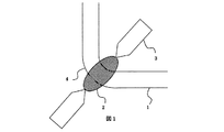
図1は、この発明の光導波路の第1の態様の概略を示す図である。すなわち、光導波路の所望部分をアーク放電により高温(屈曲店以上軟化点以下)にした状態で、光導波路を所定の半径で曲げる。この光導波路は曲げ部分は高温状態で曲げられ、曲げられた後に常温環境に持っていかれるので、曲げることによる歪はない。すなわち、曲げた状態が初期状態となるように加工したものである。光導波路は加工後に加工された状態から変形すると歪が発生して、破断するが、加工された状態を曲げ状態とすることで、歪が発生せず破断しないのである。但し、この曲げ部分を、直線状に戻す場合には歪が発生し、破断に至る。結局は、初期の歪開放状態が直線状態であるか、曲げ状態であるかを選択することで、所望の形を作成する場合の歪による破断を回避することが出来るのである。この発明では、微小な空間で光導波方向を変換することが目的であるので、変換する為の状態を初期の歪開放状態となるように加工することで、破断を回避している。
この加工を行う際に、光導波路の所望部分を加熱する方法はアーク放電による加熱、バーナーによる加熱、炉による加熱等どんな手段であっても構わず、趣旨は加熱と同時に曲げることで加工歪を開放しながら加工することである。
(実施形態2)
FIG. 1 is a diagram showing an outline of a first embodiment of an optical waveguide according to the present invention. That is, the optical waveguide is bent at a predetermined radius in a state where a desired portion of the optical waveguide is heated to a high temperature (bending store or more and softening point or less) by arc discharge. In this optical waveguide, the bent portion is bent at a high temperature, and after being bent, it is brought into a room temperature environment, so there is no distortion due to bending. That is, it is processed so that the bent state becomes the initial state. When the optical waveguide is deformed from the processed state after processing, distortion occurs and breaks, but when the processed state is changed to a bent state, no distortion occurs and the optical waveguide does not break. However, when this bent portion is returned to a straight line, distortion occurs and breaks. Eventually, by selecting whether the initial strain release state is a straight line state or a bent state, it is possible to avoid breakage due to strain when creating a desired shape. In this invention, since the purpose is to change the direction of the optical waveguide in a very small space, breakage is avoided by processing the state for conversion so as to be the initial strain release state.
When performing this processing, the method for heating the desired portion of the optical waveguide may be any means such as heating by arc discharge, heating by a burner, heating by a furnace, etc. Processing while opening.
(Embodiment 2)
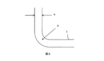
図2は、この発明の光導波路の第3及び5の態様の概略を示す図である。この態様においては、微小な空間で光導波方向を変換するが、使用する光導波路の物理的大きさから現実的に使用できる大きさが規定されている。この態様では、光導波路の外径aが50μm以上である。曲げ半径Rは、5.0mm以下である。すなわち、外径aが50μmの光導波路に対し、曲げ半径Rを50μmで曲げることは物理的に不可能である。また、外径aが50μm未満の光導波路を取り扱うのも容易ではないことから、最小外径aを50μmの光導波路を規定することで取り扱いやすさを確保し、曲げ半径として使用する光導波路の最小外径の10倍とすることで物理的に曲げを実現させる構造としている。また、外径aが125μm外径の光導波路は、現在一般に使用されている代表的な光導波路と互換な外径であるので、この外径を用いることで、本発明の適用範囲を大幅に広げられる。更に曲げ半径Rを5.0mm以下とすることで、本発明の方法を採用する利点が生かされる。すなわち、曲げ半径Rが5.0mm超では細径の光ファイバを用いた場合に、曲げ半径によっては破断歪に至らず、本発明の歪開放加工を必要としない場合があるが、曲げ半径Rを5.0mm以下とすると、取り扱いが困難とならない最小外径aを50μmとした光導波路でも、本発明の歪開放加工が必要となるのである。
この実施例では外径aが80μmである光ファイバを、曲げ半径Rを1mmにして90度に曲げている。
(実施形態3)
FIG. 2 is a diagram schematically showing the third and fifth aspects of the optical waveguide according to the present invention. In this aspect, the optical waveguide direction is converted in a minute space, but the size that can be practically used is defined from the physical size of the optical waveguide to be used. In this aspect, the outer diameter a of the optical waveguide is 50 μm or more. The bending radius R is 5.0 mm or less. That is, it is physically impossible to bend the bending radius R at 50 μm with respect to an optical waveguide having an outer diameter a of 50 μm. In addition, since it is not easy to handle an optical waveguide having an outer diameter a of less than 50 μm, by defining an optical waveguide having a minimum outer diameter a of 50 μm, it is easy to handle and an optical waveguide used as a bending radius is used. By making it 10 times the minimum outer diameter, it is configured to physically realize bending. In addition, an optical waveguide having an outer diameter a of 125 μm is an outer diameter compatible with a typical optical waveguide that is generally used at present. Therefore, by using this outer diameter, the scope of application of the present invention is greatly increased. Can be spread. Furthermore, the advantage which employ | adopts the method of this invention is utilized by making bending radius R into 5.0 mm or less. That is, when the bending radius R exceeds 5.0 mm, when a thin optical fiber is used, the bending strain does not reach the breaking strain depending on the bending radius, and the strain relief processing of the present invention may not be required. If the thickness is 5.0 mm or less, the strain relief processing of the present invention is required even for an optical waveguide having a minimum outer diameter a of 50 μm, which is difficult to handle.
In this embodiment, an optical fiber having an outer diameter a of 80 μm is bent at 90 degrees with a bending radius R of 1 mm.
(Embodiment 3)
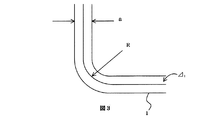
図3は、この発明の光導波路の第6の態様の概略を示す図である。実施形態2による微小な空間で光導波方向においては、機械的な破断を回避する方法に重点が置かれていたが、この態様では光学的な特性を良好に維持したまま微小な空間で光導波方向を変換することを可能にしている。光導波路のコアとクラッドの等価屈折率差Δ1が0.8%以上3.5%以下の範囲内、好ましくはΔ1が1.0%以上3.0%以下の範囲内である。すなわち、一般に使用される光導波路では、そのコアとクラッドの等価屈折率差Δ1は0.3%前後が普通である。しかし、0.3%前後の等価屈折率差Δ1の光導波路を、曲げ半径Rを5.0mm以下にして曲げると、コアに閉じ込められた光は、もはや閉じ込められなくなり、クラッドヘと放射してしまい、曲がり部分での光損失が激増する。しかし、等価屈折率差Δ1が0.8%以上3.5%以下の範囲内、好ましくはΔ1が1.0%以上3.0%以下の範囲内で、曲げ半径Rが0.5mmであっても、その曲げ部分での光損失は0.5dB以下に抑えることが可能である。3.5%超となる高い等価屈折率差Δ1にすれば、曲げ半径を0.5mm以下にしても曲げ損失をより小さく出来るが、この場合、単一モード動作を維持する為には、モードフィールド径を極端に小さくする必要が生じ、外部との接続が困難になるので、等価屈折率差Δ1は1.5%以上3.5%以下の範囲内にすることが望ましい。
この実施例では、外径aを80μm、曲げ半径Rを1mmとして90度曲げるのに、等価屈折率差Δ1を2.5%とした光ファイバを用いている。使用波長は1.3μmである。
(実施形態4)
FIG. 3 is a diagram showing an outline of the sixth embodiment of the optical waveguide of the present invention. In the optical waveguide direction in the minute space according to the second embodiment, the emphasis was placed on the method of avoiding mechanical breakage, but in this aspect, the optical waveguide is maintained in the minute space while maintaining good optical characteristics. It is possible to change the direction. Range equivalent refractive index difference delta 1 of core and clad of the optical waveguide or less 3.5% to 0.8%, preferably in the range 1 The following 3.0% and 1.0% or more delta. That is, in the optical waveguide which are commonly used, the equivalent refractive index difference delta 1 of the core and the cladding is usually 0.3% or so. However, 0.3% before and after the optical waveguide of the equivalent refractive index difference delta 1, when bending the bending radius R in the 5.0mm or less, light confined in the core is no longer confined, radiate the Kuraddohe As a result, the light loss at the bent portion increases drastically. However, when the equivalent refractive index difference Δ 1 is in the range of 0.8% to 3.5%, preferably Δ 1 is in the range of 1.0% to 3.0%, the bending radius R is 0.5 mm. Even so, the optical loss at the bent portion can be suppressed to 0.5 dB or less. If 3.5 percent to become high equivalent refractive index difference delta 1, but also bending loss with a bending radius 0.5mm or less can be smaller, in this case, in order to maintain a single mode operation, Since the mode field diameter needs to be extremely small and connection to the outside becomes difficult, it is desirable that the equivalent refractive index difference Δ 1 is in the range of 1.5% to 3.5%.
In this example, 80 [mu] m outer diameter a, to bend 90 degrees bend radius R as 1 mm, and an optical fiber in which the equivalent refractive index difference delta 1 and 2.5%. The wavelength used is 1.3 μm.
(Embodiment 4)
図4は、この発明の光導波路モジュールの第1の態様の概略を示す図である。この態様の光導波路モジュールは、本発明の光導波路をアレイ化したものであり、多数チャンネルを一括して光導波方向変換が行える。また、本発明のモジュールの入出力部分が、一般の光導波路と特性が互換の光導波路となっていることで、外部機器との特性の良い接続が可能となる。
この実施例では、外径aが80μm、等価屈折率差Δ1が2.5%の光ファイバを位置決め機構を備えた部材に固定している。また、入力から出力へは90度の光導波方向変換が行われ、研磨端面は入力と出力両方とも、90度面に対し4度ずつ傾けて研磨されている。本数は横一直線に12本が125μm間隔で並んだものである。
(実施形態5)
FIG. 4 is a diagram showing an outline of the first embodiment of the optical waveguide module of the present invention. The optical waveguide module of this embodiment is an array of the optical waveguides of the present invention, and can change the direction of the optical waveguide for a large number of channels at once. In addition, since the input / output portion of the module of the present invention is an optical waveguide whose characteristics are compatible with those of a general optical waveguide, it is possible to connect the external device with good characteristics.
In this embodiment, the outer diameter a is 80 [mu] m, the equivalent refractive index difference delta 1 is fixed to a member having a positioning mechanism 2.5% of the optical fiber. In addition, the optical waveguide direction change of 90 degrees is performed from the input to the output, and the polished end face is polished by tilting 4 degrees with respect to the 90 degree plane at both the input and output. The number is such that 12 lines are arranged in a horizontal straight line at intervals of 125 μm.
(Embodiment 5)
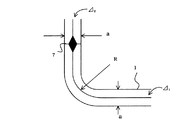
図5は、この発明の光導波路モジュールの第2の態様の概略を示す図である。この態様の光導波路モジュールは、コアとクラッドの等価屈折率差Δ1が0.8%以上3.5%以下の範囲内、好ましくはΔ1が1.0%以上3.0%以下の範囲内である第1の光導波路と、コアとクラッドの等価屈折率差Δ2が0.2%以上である第2の光導波路とを融着接続し、融着接続部分を加熱して前記コアとクラッドの等価屈折率差Δのミスマッチと、モードフィールド径のミスマッチを低減し、光導波路の所望部分を加熱して曲げる光導波路モジュールである。 FIG. 5 is a diagram showing an outline of the second mode of the optical waveguide module of the present invention. In the optical waveguide module of this aspect, the equivalent refractive index difference Δ 1 between the core and the clad is in the range of 0.8% to 3.5%, preferably Δ 1 is in the range of 1.0% to 3.0%. a first optical waveguide and a second optical waveguide equivalent refractive index difference delta 2 of the core and the cladding is 0.2% or more fusion splicing is an internal, said core by heating the fusion spliced portion This is an optical waveguide module that reduces the mismatch of the equivalent refractive index difference Δ and the clad and the mismatch of the mode field diameter, and heats and bends a desired portion of the optical waveguide.
すなわち、第2の態様による光導波路モジュールでは、高い等価屈折率差の光導波路を使用するため、そのコアやクラッドの等価屈折率は一般の光導波路のコアやクラッドの等価屈折率とは異なる。また、等価屈折率差Δも異なる為、一般の光導波路のモードフィールド径と、本発明の光導波方向変換部に使用する光導波路のモードフィールド径との間に差がある。屈折率の異なるもの同士を接触させて、その部分に光信号を通過させると、屈折率の境界部分で光が反射される。これは、光通信においては避けなければならない現象である。一般にこの反射減衰量として50dB以上が要求される。 That is, in the optical waveguide module according to the second aspect, since an optical waveguide having a high equivalent refractive index difference is used, the equivalent refractive index of the core or cladding is different from the equivalent refractive index of the core or cladding of a general optical waveguide. Also, since the equivalent refractive index difference Δ is different, there is a difference between the mode field diameter of a general optical waveguide and the mode field diameter of the optical waveguide used in the optical waveguide direction changing portion of the present invention. When objects having different refractive indexes are brought into contact with each other and an optical signal is passed through that portion, light is reflected at the boundary portion of the refractive index. This is a phenomenon that must be avoided in optical communication. Generally, the return loss is required to be 50 dB or more.
また、モードフィールド径が異なるもの同士を接続した場合、接続部分では径差による接続損失が発生する。一般の光導波路のモードフィールド径は使用波長によっても異なるが、約10μm程度であり、本発明の光導波方向変換部に使用する光導波路のモードフィールド径は約3μmである。この径差でそのまま接続すると、接続損失は5dB以上となる。また、外部の機器やレーザーとの接続を容易にする為には、一般の光ファイバと外部機器を接続し、その後、本発明の光導波方向変換部に接続することが、有効である。そこで、第2の態様では、これらの反射、接続損失を低減する為、コアとクラッドの等価屈折率差Δ1が0.8%以上3.5%以下の範囲内、好ましくは1.0%以上3.0%以下の範囲内である第1の光導波路と、コアとクラッドの等価屈折率差Δ2が0.2%以上である第2の光導波路とを融着接続し、融着接続部分を加熱してコアとクラッドの等価屈折率差Δのミスマッチとモードフィールド径のミスマッチを低減させることで、反射減衰量を大きくし、接続損失を抑制している。この方法によって、反射減衰量は50dB以上となり、接続損失は約0.2dBとなった。 In addition, when devices having different mode field diameters are connected to each other, a connection loss due to a diameter difference occurs at the connection portion. Although the mode field diameter of a general optical waveguide varies depending on the wavelength used, it is about 10 μm, and the mode field diameter of the optical waveguide used in the optical waveguide direction changing portion of the present invention is about 3 μm. If the connection is made with this diameter difference, the connection loss is 5 dB or more. In order to facilitate connection with an external device or a laser, it is effective to connect a general optical fiber and an external device, and then connect to the optical waveguide direction changer of the present invention. In the second aspect, these reflections, to reduce the connection loss, the core and the equivalent refractive index difference delta 1 of the cladding is within the range of 3.5% to 0.8%, preferably 1.0% or a first optical waveguide is 3.0% within the range, and a second optical waveguide equivalent refractive index difference delta 2 of the core and the cladding is 0.2% or more fusion spliced, fusing By heating the connection portion and reducing the mismatch of the equivalent refractive index difference Δ between the core and the clad and the mismatch of the mode field diameter, the return loss is increased and the connection loss is suppressed. By this method, the return loss was 50 dB or more, and the connection loss was about 0.2 dB.
この実施例では、外径aが80μm、曲げ半径Rが1mmで90度曲げるのに、等価屈折率差Δ1を2.5%で、使用波長による光導波モードが単一モードとなる光ファイバを用いて、その片側に外径aが80μm、等価屈折率差Δ20.35%で、使用波長による光導波モードが単一モードとなる光ファイバとを融着接続し、融着接続部分をガスバーナーで加熱して等価屈折率差Δのミスマッチとモードフィールド径のミスマッチを低滅させた。使用波長は1.3μmである。測定結果では反射減衰量が50dB以上、接続損失は0.2dBであった。
(実施形態6)
In this embodiment, an optical fiber in which the optical waveguide mode depending on the wavelength used is a single mode even when the outer diameter a is 80 μm and the bending radius R is 1 mm and the optical fiber is bent by 90 degrees and the equivalent refractive index difference Δ 1 is 2.5%. And an optical fiber having an outer diameter a of 80 μm, an equivalent refractive index difference Δ 2 of 0.35%, and an optical waveguide mode depending on the used wavelength being a single mode. Was heated with a gas burner to reduce the mismatch of the equivalent refractive index difference Δ and the mismatch of the mode field diameter. The wavelength used is 1.3 μm. According to the measurement results, the return loss was 50 dB or more, and the connection loss was 0.2 dB.
(Embodiment 6)
図6も、この発明の光導波路モジュールの第2の態様の概略を示す図である。この態様の光導波路モジュールは、コアとクラッドの等価屈折率差Δ1が0.8%以上3.5%以下の範囲内、好ましくは1.0%以上3.0%以下の範囲内である第1の光導波路の両端に、コアとクラッドの等価屈折率差Δ2が0.2%以上である第2の光導波路とを融着接続し、融着接続部分を加熱して前記コアとクラッドの等価屈折率差Δのミスマッチと、モードフィールド径のミスマッチを低減し、光導波路の所望部分を加熱して曲げる光導波路モジュールである。これは実施形態5において、光導波方向変換部の片側にだけ一般の光導波路の特性と互換な光導波路を融着接続して、接続部を加熱することで等価屈折率差Δのミスマッチとモードフィールド径のミスマッチを低減させたが、実施形態6では光導波方向変換部の両側に一般の光導波路の特性と互換な光導波路を融着接続して、接続部を加熱することで等価屈折率差Δのミスマッチとモードフィールド径のミスマッチを低減させる。これにより、光導波方向変換部のどちら側も、外部機器との接続が容易となる。
FIG. 6 is also a diagram showing an outline of the second mode of the optical waveguide module of the present invention. Optical waveguide module of this embodiment, the range equivalent refractive index difference delta 1 of core and cladding or less 3.5% to 0.8%, is preferably in the range of 3.0% or less than 1.0% at both ends of the first optical waveguide and a second optical waveguide equivalent refractive index difference delta 2 of the core and the cladding is 0.2% or more fused connection, said core by heating the fusion spliced portion This is an optical waveguide module that reduces the mismatch of the equivalent refractive index difference Δ of the clad and the mismatch of the mode field diameter and heats and bends a desired portion of the optical waveguide. In the fifth embodiment, an optical waveguide compatible with the characteristics of a general optical waveguide is fused and connected only to one side of the optical waveguide direction changing section, and the equivalent refractive index difference Δ is mismatched and mode by heating the connecting section. Although the mismatch of the field diameter is reduced, in
この実施例では外径aが80μm、曲げ半径Rが1mmで90度曲げるのに、等価屈折率差Δ1を2.5%、使用波長による光導波モードが単一モードとなる光ファイバを用いて、その両側に外径aが80μm、等価屈折率差Δ2が0.35%、使用波長による光導波モードが単一モードとなる光ファイバを融着接続し、融着接続部分をガスバーナーで加熱して、等価屈折率差Δのミスマッチとモードフィールド径のミスマッチを低減させた。使用波長は1.3μmである。測定結果では反射減衰量が50dB以上、接続損失は0.4dB程度であった。
(実施形態7)
Outer diameter a is 80μm in this embodiment, although the bending radius R is bent 90 degrees at 1 mm, the equivalent refractive index difference delta 1 2.5%, using an optical fiber optical waveguide mode by using wavelength is single mode An optical fiber having an outer diameter a of 80 μm, an equivalent refractive index difference Δ 2 of 0.35%, and an optical waveguide mode depending on the wavelength used is a single mode on both sides, and the fusion spliced portion is a gas burner. To reduce the mismatch of the equivalent refractive index difference Δ and the mismatch of the mode field diameter. The wavelength used is 1.3 μm. According to the measurement results, the return loss was 50 dB or more, and the connection loss was about 0.4 dB.
(Embodiment 7)
図7は、この発明の光導波路モジュールの第4から6の態様の概略を示す図である。この発明により、光導波路モジュールを作製するに際し、シートに内蔵される光導波路のコアとクラッドの等価屈折率差Δ1を0.8%以上3.5%以下の範囲内とした。
この実施例では、ガラス部分の外径125μm、被覆外径250μmの一般的な外径の光ファイバを使用しているが、コアとクラッドの等価屈折率差Δ1は2.5%と一般的な単一モード光ファイバの等価屈折率差Δ1である0.3%程度とは異なる、非常に大きな等価屈折率差Δ1の光導波路を使用している。
FIG. 7 is a diagram showing an outline of fourth to sixth embodiments of the optical waveguide module of the present invention. This invention, when producing an optical waveguide module, the core and the equivalent refractive index difference delta 1 of the cladding of the optical waveguide which is incorporated in the sheet was in the range of 3.5% or less 0.8% or more.
In this embodiment, an optical fiber having a general outer diameter with an outer diameter of the glass portion of 125 μm and a coating outer diameter of 250 μm is used, but the equivalent refractive index difference Δ 1 between the core and the cladding is generally 2.5%. An optical waveguide having a very large equivalent refractive index difference Δ 1 is used, which is different from about 0.3% which is the equivalent refractive index difference Δ 1 of such a single mode optical fiber.
このような、一般的な単一モード光ファイバの等価屈折率差Δ1と比較して大きな等価屈折率差Δ1を持った光ファイバを用いて光導波路モジュールを作製すると、光導波路モジュールにうねりや曲げが加わっても、それによるロスが低減される。具体的には、一般の光ファイバを用いた光導波路モジュールを、2枚のサンドペーパーで挟み込んで押し付け、その状態のまま−40℃〜+80℃の温度サイクルによる損失変動試験を行った結果では、−40℃の低温時に損失が最大約20dBという、非常に悪い結果であったのに対し、等価屈折率差Δ1が2.5%であること以外は全く条件が同じ光導波路モジュールで、全く同様の試験を行った結果では、−40℃〜+80℃の温度サイクルによる損失変動最大値は約0.1dBであり、殆ど損失変動が現れない。 Such, when producing an optical waveguide module using a typical single-mode optical fiber having a large equivalent refractive index difference delta 1 as compared to the equivalent refractive index difference delta 1 of the fiber, it swells the optical waveguide module Even if bending is applied, the resulting loss is reduced. Specifically, an optical waveguide module using a general optical fiber is sandwiched and pressed between two pieces of sandpaper, and as a result of performing a loss variation test by a temperature cycle of −40 ° C. to + 80 ° C. in that state, loss at a low temperature of -40 ℃ is that up to about 20 dB, whereas was very poor results, with the same optical waveguide module at all conditions except that the equivalent refractive index difference delta 1 is 2.5%, quite As a result of performing the same test, the maximum loss variation due to the temperature cycle of −40 ° C. to + 80 ° C. is about 0.1 dB, and the loss variation hardly appears.
等価屈折率差Δ1を1.5%まで低くしても、上記試験での損失変動はやはり約0.1dB程度であった。しかし、それ以下の等価屈折率差Δ1では、段々と損失変動が大きくなり、等価屈折率差Δ1が1%になると、前記試験での損失変動は最大で0.5dB程度となった。0.5dBでも実用上の問題は無いが、本発明の光導波路モジュールは前発明の光導波方向変換素子と接続して使用することで、良好な光伝送特性と接続特性を有する電気光融合回路基板を実現させることが可能であるので、前発明の光導波方向変換素子との接続性を考慮して、前発明の光導波方向変換素子で用いた等価屈折率差Δ1の最低値である1.5%以上と規定した。 Even when the equivalent refractive index difference delta 1 was lowered to 1.5%, the loss fluctuation in the above test was also about 0.1 dB. However, when the equivalent refractive index difference Δ 1 is less than that, the loss fluctuation gradually increases, and when the equivalent refractive index difference Δ 1 is 1%, the loss fluctuation in the test is about 0.5 dB at the maximum. Although there is no practical problem even at 0.5 dB, the optical waveguide module of the present invention is used by connecting to the optical waveguide direction changing element of the previous invention, so that the electro-optical fusion circuit having good optical transmission characteristics and connection characteristics Since the substrate can be realized, it is the lowest value of the equivalent refractive index difference Δ 1 used in the optical waveguide direction change element of the previous invention in consideration of the connectivity with the optical waveguide direction change element of the previous invention. It was defined as 1.5% or more.
また、等価屈折率差Δ1が大きくなれば損失変動は小さくなるが、等価屈折率差Δ1を大きくしすぎると、光ファイバ中のモードフィールド径が小さくなり、接続時の高精度な位置精度が求められるようになることと、前発明の光導波方向変換素子との接続性を考慮してΔ1は3.5%以下とした。 Further, if the equivalent refractive index difference Δ 1 is increased, the loss fluctuation is reduced. However, if the equivalent refractive index difference Δ 1 is excessively increased, the mode field diameter in the optical fiber is reduced, and the position accuracy is high at the time of connection. and a to become to be required, the delta 1 in consideration of the connectivity with the optical waveguide direction converting element of the prior invention was 3.5% or less.
機械的に小さく曲げられるようにするには、ガラス部分の外径aをもっと小さくすれば良いが、外径を小さくしすぎると、コアに閉じ込められた光がクラッドが薄すぎるため逃げ出してしまい、伝送損失を発生する。そこで、クラッド径すなわち光ファイバ外径はモードフィールド径の少なくとも10倍以上とすることで、この伝送損失を抑えることが可能となる。 In order to bend mechanically small, the outer diameter a of the glass portion may be made smaller, but if the outer diameter is made too small, the light trapped in the core will escape because the cladding is too thin, Transmission loss occurs. Therefore, the transmission loss can be suppressed by setting the cladding diameter, that is, the optical fiber outer diameter, to at least 10 times the mode field diameter.
また、細くすることで、本形態で行ったような−40℃〜+80℃の温度サイクルによる損失変動試験には弱くなってしまうが、等価屈折率差Δ1が1.5%以上では光ファイバの外径aを50μmとした、モードフィールド径が5μmのファイバでは、最大損失変動は0.1dB程度と、非常に良好な特性を維持していることが確認された。
(実施形態8)
In addition, thinning makes the loss fluctuation test due to a temperature cycle of −40 ° C. to + 80 ° C. as performed in this embodiment weak, but if the equivalent refractive index difference Δ 1 is 1.5% or more, the optical fiber It was confirmed that the fiber having a mode field diameter of 5 μm with an outer diameter a of 50 μm maintained a very good characteristic with a maximum loss fluctuation of about 0.1 dB.
(Embodiment 8)
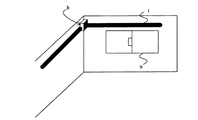
図8は、この発明の光導波路モジュールを宅内での角配線に適用した概念図である。このように、宅内の部屋の角などでの光導波路の配線は、従来光導波路の最小曲げ半径である数cmを確保する必要があったが、本発明の光導波路モジュールを用いることで、モジュールサイズとしても1cm以下の大きさで角配線が可能となった。なお、図8のbは90度で曲げることが可能となったことを示している。
(実施形態9)
FIG. 8 is a conceptual diagram in which the optical waveguide module according to the present invention is applied to corner wiring in a home. As described above, the wiring of the optical waveguide at the corner of the room in the house had to secure several centimeters which is the minimum bending radius of the conventional optical waveguide, but the module can be obtained by using the optical waveguide module of the present invention. As for the size, the corner wiring can be made with a size of 1 cm or less. In addition, b of FIG. 8 has shown that it became possible to bend at 90 degree | times.
(Embodiment 9)
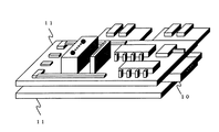
図9は、本発明の光導波路モジュールを電気光回路融合基板に適用した概略を示す図である。電気光融合基板は2枚の電気回路基板に光導波路モジュールがサンドイッチされた構造となっており、光導波路モジュールの電気回路基板面への90度方向光導波方向変換部端部にこの発明の光導波路モジュールが取り付けられている。 FIG. 9 is a diagram showing an outline in which the optical waveguide module of the present invention is applied to an electro-optical circuit fusion substrate. The electro-optical fusion substrate has a structure in which the optical waveguide module is sandwiched between two electric circuit substrates, and the optical waveguide of the present invention is formed at the end of the 90 ° direction optical waveguide direction conversion portion toward the electric circuit substrate surface of the optical waveguide module. A waveguide module is attached.
本発明の光導波路により、融着接続による接続損失を低減させながら、所望部分を所望の半径で曲げて、所定の角度に光導波方向を変換することができる。さらに、それらを用いて光導波路モジュールの小型化が可能となり、産業上の利用価値が高い。 With the optical waveguide of the present invention, the optical waveguide direction can be converted to a predetermined angle by bending a desired portion with a desired radius while reducing connection loss due to fusion splicing. Furthermore, it is possible to reduce the size of the optical waveguide module by using them, and the industrial utility value is high.
1 光ファイバ
2 アーク放電
3 電極
4 所望部分
5 位置決め機構
6 部材
7 融着接続部
8 シート
9 窓
10 光導波路モジュール
11 電気光回路融合基板
DESCRIPTION OF
Claims (13)
当該加工歪開放状態に移行した前記部分を所定の曲げ半径で曲線状に曲げられて、加工歪状態に移行していることを特徴とする光導波路。 An optical waveguide having a core and a clad, where a desired portion is heated and shifted to a processing strain release state,
An optical waveguide, wherein the portion that has shifted to the processing strain release state is bent into a curved shape with a predetermined bending radius, and shifts to a processing strain state.
前記光導波路の前記部分を加工歪開放状態に移行し、
加工歪開放状態に移行した前記光導波炉の前記部分を所定の曲げ半径に曲げ、
所定の曲げ半径に曲げた状態で前記光導波路の前記部分を加工歪状態に移行する
ことを特徴とする光導波路の作成方法。
Heating the desired part of the optical waveguide,
The portion of the optical waveguide is shifted to a processing strain release state,
Bending the portion of the optical waveguide furnace that has shifted to the processing strain release state to a predetermined bending radius,
A method for producing an optical waveguide, wherein the portion of the optical waveguide is shifted to a working strain state while being bent to a predetermined bending radius.
Priority Applications (6)
| Application Number | Priority Date | Filing Date | Title |
|---|---|---|---|
| JP2004111211A JP2005292718A (en) | 2004-04-05 | 2004-04-05 | Optical waveguide, optical waveguide module, and method for producing optical waveguide |
| CN2005800178183A CN1973221B (en) | 2004-04-05 | 2005-03-30 | Optical waveguide, optical waveguide module, and method for manufacturing optical waveguide |
| PCT/JP2005/006169 WO2005098490A1 (en) | 2004-04-05 | 2005-03-30 | Optical waveguide, optical waveguide module and method for forming optical waveguide |
| US11/547,610 US20070183730A1 (en) | 2004-04-05 | 2005-03-30 | Optical waveguide, optical waveguide module and method for forming optical waveguide |
| EP05727267A EP1736805A4 (en) | 2004-04-05 | 2005-03-30 | Optical waveguide, optical waveguide module and method for forming optical waveguide |
| US13/016,580 US8014644B2 (en) | 2004-04-05 | 2011-01-28 | Optical waveguide, optical waveguide module and method for forming optical waveguide |
Applications Claiming Priority (1)
| Application Number | Priority Date | Filing Date | Title |
|---|---|---|---|
| JP2004111211A JP2005292718A (en) | 2004-04-05 | 2004-04-05 | Optical waveguide, optical waveguide module, and method for producing optical waveguide |
Publications (1)
| Publication Number | Publication Date |
|---|---|
| JP2005292718A true JP2005292718A (en) | 2005-10-20 |
Family
ID=35125215
Family Applications (1)
| Application Number | Title | Priority Date | Filing Date |
|---|---|---|---|
| JP2004111211A Pending JP2005292718A (en) | 2004-04-05 | 2004-04-05 | Optical waveguide, optical waveguide module, and method for producing optical waveguide |
Country Status (5)
| Country | Link |
|---|---|
| US (2) | US20070183730A1 (en) |
| EP (1) | EP1736805A4 (en) |
| JP (1) | JP2005292718A (en) |
| CN (1) | CN1973221B (en) |
| WO (1) | WO2005098490A1 (en) |
Cited By (10)
| Publication number | Priority date | Publication date | Assignee | Title |
|---|---|---|---|---|
| JP2009244750A (en) * | 2008-03-31 | 2009-10-22 | Furukawa Electric Co Ltd:The | Fiber bent connector component, and manufacturing method therefor |
| JP2009244612A (en) * | 2008-03-31 | 2009-10-22 | Furukawa Electric Co Ltd:The | Optical waveguide attaching component, optical waveguide connector, and method for manufacturing optical waveguide connector |
| JP2010049173A (en) * | 2008-08-25 | 2010-03-04 | Tomoegawa Paper Co Ltd | Optical connection structure |
| CN102005688A (en) * | 2010-09-17 | 2011-04-06 | 山东大学 | Method for preparing slab waveguide laser device in neodymium-doped lutecium vanadate crystal |
| JP2013047856A (en) * | 2006-11-20 | 2013-03-07 | Furukawa Electric Co Ltd:The | Optical waveguide component and method for manufacturing optical waveguide component |
| JP2013238721A (en) * | 2012-05-15 | 2013-11-28 | Sumitomo Electric Ind Ltd | Multi-core optical fiber mounting method |
| JP2017021360A (en) * | 2016-09-07 | 2017-01-26 | 住友電気工業株式会社 | Conversion element |
| US9594220B1 (en) | 2015-09-22 | 2017-03-14 | Corning Optical Communications LLC | Optical interface device having a curved waveguide using laser writing and methods of forming |
| US9766411B2 (en) | 2015-11-20 | 2017-09-19 | Corning Optical Communications LLC | Optical interface devices and methods employing optical fibers and a support member having a bend section |
| US10036856B2 (en) | 2014-07-11 | 2018-07-31 | Furukawa Electric Co., Ltd. | Connector with built-in bent optical fibers and method for producing bent optical fibers |
Families Citing this family (62)
| Publication number | Priority date | Publication date | Assignee | Title |
|---|---|---|---|---|
| CA2559228C (en) | 2004-04-21 | 2016-06-21 | Enobia Pharma Inc. | Bone delivery conjugates and method of using same to target proteins to bone |
| CN102187255B (en) * | 2008-10-17 | 2013-06-12 | 株式会社巴川制纸所 | Optical transmission medium forming method, optical transmission medium forming device, and optical transmission medium manufacturing method |
| US8905610B2 (en) | 2009-01-26 | 2014-12-09 | Flex Lighting Ii, Llc | Light emitting device comprising a lightguide film |
| CN102449516A (en) | 2009-04-28 | 2012-05-09 | 惠普开发有限公司 | Angled Connectors for Fiber Optics |
| US20100284656A1 (en) * | 2009-05-07 | 2010-11-11 | Ofs Fitel, Llc | Short profile optical connector |
| PT2432489T (en) | 2009-05-20 | 2016-12-07 | Biomarin Pharm Inc | Variants of c-type natriuretic peptide |
| US8125856B1 (en) * | 2009-11-05 | 2012-02-28 | Western Digital (Fremont), Llc | Method and system for optically coupling a laser with a transducer in an energy assisted magnetic recording disk drive |
| US9651729B2 (en) | 2010-04-16 | 2017-05-16 | Flex Lighting Ii, Llc | Reflective display comprising a frontlight with extraction features and a light redirecting optical element |
| US20140049983A1 (en) | 2010-11-18 | 2014-02-20 | Anthony John Nichol | Light emitting device comprising a lightguide film and aligned coupling lightguides |
| WO2012088608A1 (en) | 2010-12-27 | 2012-07-05 | Enobia Canada Limited Partnership | Compositions comprising natriuretic peptides and methods of use thereof |
| CA2829388C (en) | 2011-03-09 | 2018-09-25 | Flex Lighting Ii, Llc | Light emitting device with adjustable light output profile |
| JP6038882B2 (en) * | 2011-04-20 | 2016-12-07 | マッパー・リソグラフィー・アイピー・ビー.ブイ. | Optical fiber constructs and methods of forming such constructs |
| KR20140084201A (en) | 2011-10-19 | 2014-07-04 | 알렉시온 파마 홀딩 | Compositions comprising alkaline phosphatase and/or natriuretic peptide and methods of use thereof |
| US9134807B2 (en) | 2012-03-02 | 2015-09-15 | Microsoft Technology Licensing, Llc | Pressure sensitive key normalization |
| US9075566B2 (en) | 2012-03-02 | 2015-07-07 | Microsoft Technoogy Licensing, LLC | Flexible hinge spine |
| US20130300590A1 (en) | 2012-05-14 | 2013-11-14 | Paul Henry Dietz | Audio Feedback |
| US10052366B2 (en) | 2012-05-21 | 2018-08-21 | Alexion Pharmaceuticsl, Inc. | Compositions comprising alkaline phosphatase and/or natriuretic peptide and methods of use thereof |
| US11009646B2 (en) | 2013-03-12 | 2021-05-18 | Azumo, Inc. | Film-based lightguide with interior light directing edges in a light mixing region |
| US9690032B1 (en) * | 2013-03-12 | 2017-06-27 | Flex Lighting Ii Llc | Lightguide including a film with one or more bends |
| JP6268977B2 (en) * | 2013-11-25 | 2018-01-31 | 住友電気工業株式会社 | Manufacturing method of bent optical fiber |
| WO2016007873A1 (en) | 2014-07-11 | 2016-01-14 | The Regents Of The University Of Michigan | Compositions and methods for treating craniosynostosis |
| US9304235B2 (en) | 2014-07-30 | 2016-04-05 | Microsoft Technology Licensing, Llc | Microfabrication |
| US10324733B2 (en) | 2014-07-30 | 2019-06-18 | Microsoft Technology Licensing, Llc | Shutdown notifications |
| US10678412B2 (en) | 2014-07-31 | 2020-06-09 | Microsoft Technology Licensing, Llc | Dynamic joint dividers for application windows |
| US10254942B2 (en) | 2014-07-31 | 2019-04-09 | Microsoft Technology Licensing, Llc | Adaptive sizing and positioning of application windows |
| US9787576B2 (en) | 2014-07-31 | 2017-10-10 | Microsoft Technology Licensing, Llc | Propagating routing awareness for autonomous networks |
| US10592080B2 (en) | 2014-07-31 | 2020-03-17 | Microsoft Technology Licensing, Llc | Assisted presentation of application windows |
| MX389350B (en) | 2014-12-05 | 2025-03-19 | Alexion Pharma Inc | RECOMBINANT ALKALINE PHOSPHATASES AND THEIR USES FOR THE TREATMENT OF SEIZURES. |
| JP6868561B2 (en) | 2015-01-28 | 2021-05-12 | アレクシオン ファーマシューティカルズ, インコーポレイテッド | How to treat subjects with alkaline phosphatase deficiency |
| US9513480B2 (en) | 2015-02-09 | 2016-12-06 | Microsoft Technology Licensing, Llc | Waveguide |
| US9423360B1 (en) | 2015-02-09 | 2016-08-23 | Microsoft Technology Licensing, Llc | Optical components |
| US10018844B2 (en) | 2015-02-09 | 2018-07-10 | Microsoft Technology Licensing, Llc | Wearable image display system |
| US9372347B1 (en) | 2015-02-09 | 2016-06-21 | Microsoft Technology Licensing, Llc | Display system |
| US9429692B1 (en) | 2015-02-09 | 2016-08-30 | Microsoft Technology Licensing, Llc | Optical components |
| US11086216B2 (en) | 2015-02-09 | 2021-08-10 | Microsoft Technology Licensing, Llc | Generating electronic components |
| US10317677B2 (en) | 2015-02-09 | 2019-06-11 | Microsoft Technology Licensing, Llc | Display system |
| US9535253B2 (en) | 2015-02-09 | 2017-01-03 | Microsoft Technology Licensing, Llc | Display system |
| US9827209B2 (en) | 2015-02-09 | 2017-11-28 | Microsoft Technology Licensing, Llc | Display system |
| DE112015006766T5 (en) * | 2015-08-04 | 2018-04-19 | Sumitomo Electric Industries, Ltd. | Optical connection component |
| CN108350440A (en) | 2015-08-17 | 2018-07-31 | 阿雷克森制药公司 | Manufacture of Alkaline Phosphates |
| JP6868617B2 (en) | 2015-09-28 | 2021-05-12 | アレクシオン ファーマシューティカルズ, インコーポレイテッド | Identifying effective dosing regimens for tissue-nonspecific alkaline phosphatase (TNSALP) enzyme replacement therapy for hypophosphataseemia |
| JP2018533571A (en) | 2015-10-30 | 2018-11-15 | アレクシオン ファーマシューティカルズ, インコーポレイテッド | Methods for treating cranial suture early healing disease in a patient |
| WO2017155569A1 (en) | 2016-03-08 | 2017-09-14 | Alexion Pharmaceuticals, Inc. | Methods for treating hypophosphatasia in children |
| JP7613826B2 (en) | 2016-04-01 | 2025-01-15 | アレクシオン ファーマシューティカルズ, インコーポレイテッド | Treating muscle weakness with alkaline phosphatase |
| US10898549B2 (en) | 2016-04-01 | 2021-01-26 | Alexion Pharmaceuticals, Inc. | Methods for treating hypophosphatasia in adolescents and adults |
| US10988744B2 (en) | 2016-06-06 | 2021-04-27 | Alexion Pharmaceuticals, Inc. | Method of producing alkaline phosphatase |
| WO2018011991A1 (en) * | 2016-07-15 | 2018-01-18 | 住友電気工業株式会社 | Method for manufacturing optical connection component |
| EP3500289B1 (en) | 2016-08-18 | 2024-10-09 | Alexion Pharmaceuticals, Inc. | Asfotase alfa for use in treating tracheobronchomalacia |
| JP6834254B2 (en) | 2016-08-30 | 2021-02-24 | 住友電気工業株式会社 | Manufacturing method of bent optical fiber |
| US10422950B2 (en) | 2017-02-20 | 2019-09-24 | Corning Optical Communications LLC | Laminated glass bend optical interconnection apparatus and methods |
| EP3600383A4 (en) | 2017-03-31 | 2020-10-28 | Alexion Pharmaceuticals, Inc. | METHODS FOR TREATMENT OF HYPOPHOSPHATASIA (HPP) IN ADULTS AND ADOLESCENTS |
| US11913039B2 (en) | 2018-03-30 | 2024-02-27 | Alexion Pharmaceuticals, Inc. | Method for producing recombinant alkaline phosphatase |
| US12268733B2 (en) | 2018-08-10 | 2025-04-08 | Alexion Pharmaceuticals, Inc. | Methods of treating neurofibromatosis type 1 and related conditions with alkaline phosphatase |
| WO2020047340A1 (en) | 2018-08-30 | 2020-03-05 | Flex Lighting Ii, Llc | Film-based frontlight with angularly varying diffusion film |
| CN113678034B (en) | 2018-12-11 | 2024-03-19 | 阿祖莫公司 | Method for fabricating displays using thin film-based light guides and diffuse reflective release liners |
| CN113678035B (en) | 2019-01-03 | 2024-10-18 | 阿祖莫公司 | Reflective display including a light guide and a light turning film producing multiple illumination peaks |
| WO2020146668A1 (en) | 2019-01-09 | 2020-07-16 | Flex Lighting Ii, Llc | Reflective display comprising coupling lightguides folded at different fold angles |
| US11513274B2 (en) | 2019-08-01 | 2022-11-29 | Azumo, Inc. | Lightguide with a light input edge between lateral edges of a folded strip |
| CA3161266A1 (en) | 2019-12-09 | 2021-06-17 | Alexion Pharmaceuticals, Inc. | Alkaline phosphatase polypeptides and methods of use thereof |
| AU2021337652B2 (en) | 2020-09-04 | 2025-01-30 | Alexion Pharmaceuticals, Inc. | Methods for treating bone mineralization disorders |
| WO2022072386A1 (en) | 2020-09-29 | 2022-04-07 | Azumo, Inc | Manufacturing a lightguide with cut lateral edges |
| BR112023016048A2 (en) | 2021-02-12 | 2023-11-14 | Alexion Pharma Inc | ALKALINE PHOSPHATASE POLYPEPTIDES AND METHODS OF USE THEREOF |
Family Cites Families (17)
| Publication number | Priority date | Publication date | Assignee | Title |
|---|---|---|---|---|
| US4389090A (en) * | 1980-09-04 | 1983-06-21 | The Board Of Trustees Of Leland Stanford Jr. Univ. | Fiber optic polarization controller |
| US4444460A (en) * | 1981-05-26 | 1984-04-24 | Gould Inc. | Optical fiber apparatus including subtstrate ruggedized optical fibers |
| JPS5898706A (en) * | 1981-12-07 | 1983-06-11 | Sumitomo Electric Ind Ltd | Manufacture of plastic optical fiber |
| WO1987005117A1 (en) * | 1986-02-20 | 1987-08-27 | The Dow Chemical Company | Polymeric optical fiber |
| US4812001A (en) * | 1987-07-28 | 1989-03-14 | Raychem Corp. | Annealing bent optical fiber |
| US4875969A (en) * | 1988-10-07 | 1989-10-24 | Eastman Kodak Company | Method of making a fiber optic array |
| US5138676A (en) | 1990-06-15 | 1992-08-11 | Aster Corporation | Miniature fiberoptic bend device and method |
| EP0733600B1 (en) * | 1991-08-26 | 2000-01-12 | Nippon Telegraph And Telephone Corporation | Optical fiber for optical amplifier |
| US5553177A (en) * | 1992-01-15 | 1996-09-03 | Ceramoptec Industries, Inc. | Optical fiber device which increases light intensity |
| JPH05319843A (en) * | 1992-05-18 | 1993-12-03 | Fujitsu Ltd | Production of curved optical waveguide substrate |
| AU753662B2 (en) | 1998-08-25 | 2002-10-24 | Alcoa Fujikura Limited | Asymmetrical miniature bends in optical fibers and methods of forming same |
| JP2000329950A (en) | 1999-05-24 | 2000-11-30 | Fujikura Ltd | Flexible optical fiber sheet |
| CA2311966A1 (en) * | 1999-06-23 | 2000-12-23 | Stavros Dariotis | Optical fiber mach-zehnder interferometer employing miniature bends |
| US6612753B1 (en) | 1999-08-11 | 2003-09-02 | Alcoa Fujikura Ltd. | Miniature bend splice in optical fibers and method of forming same |
| JP2002202429A (en) * | 2000-12-28 | 2002-07-19 | Sumitomo Electric Ind Ltd | Optical fiber connection method and optical transmission line |
| US6904197B2 (en) * | 2002-03-04 | 2005-06-07 | Corning Incorporated | Beam bending apparatus and method of manufacture |
| JP3866172B2 (en) * | 2002-08-27 | 2007-01-10 | 富士通株式会社 | Optical module and fiber sheet |
-
2004
- 2004-04-05 JP JP2004111211A patent/JP2005292718A/en active Pending
-
2005
- 2005-03-30 CN CN2005800178183A patent/CN1973221B/en not_active Expired - Fee Related
- 2005-03-30 WO PCT/JP2005/006169 patent/WO2005098490A1/en not_active Ceased
- 2005-03-30 EP EP05727267A patent/EP1736805A4/en not_active Ceased
- 2005-03-30 US US11/547,610 patent/US20070183730A1/en not_active Abandoned
-
2011
- 2011-01-28 US US13/016,580 patent/US8014644B2/en not_active Expired - Lifetime
Cited By (11)
| Publication number | Priority date | Publication date | Assignee | Title |
|---|---|---|---|---|
| JP2013047856A (en) * | 2006-11-20 | 2013-03-07 | Furukawa Electric Co Ltd:The | Optical waveguide component and method for manufacturing optical waveguide component |
| JP2009244750A (en) * | 2008-03-31 | 2009-10-22 | Furukawa Electric Co Ltd:The | Fiber bent connector component, and manufacturing method therefor |
| JP2009244612A (en) * | 2008-03-31 | 2009-10-22 | Furukawa Electric Co Ltd:The | Optical waveguide attaching component, optical waveguide connector, and method for manufacturing optical waveguide connector |
| JP2010049173A (en) * | 2008-08-25 | 2010-03-04 | Tomoegawa Paper Co Ltd | Optical connection structure |
| CN102005688A (en) * | 2010-09-17 | 2011-04-06 | 山东大学 | Method for preparing slab waveguide laser device in neodymium-doped lutecium vanadate crystal |
| JP2013238721A (en) * | 2012-05-15 | 2013-11-28 | Sumitomo Electric Ind Ltd | Multi-core optical fiber mounting method |
| US10036856B2 (en) | 2014-07-11 | 2018-07-31 | Furukawa Electric Co., Ltd. | Connector with built-in bent optical fibers and method for producing bent optical fibers |
| US9594220B1 (en) | 2015-09-22 | 2017-03-14 | Corning Optical Communications LLC | Optical interface device having a curved waveguide using laser writing and methods of forming |
| US9784930B2 (en) | 2015-09-22 | 2017-10-10 | Corning Optical Communications LLC | Optical interface device having a curved waveguide using laser writing and methods of forming |
| US9766411B2 (en) | 2015-11-20 | 2017-09-19 | Corning Optical Communications LLC | Optical interface devices and methods employing optical fibers and a support member having a bend section |
| JP2017021360A (en) * | 2016-09-07 | 2017-01-26 | 住友電気工業株式会社 | Conversion element |
Also Published As
| Publication number | Publication date |
|---|---|
| US8014644B2 (en) | 2011-09-06 |
| US20110135261A1 (en) | 2011-06-09 |
| EP1736805A4 (en) | 2007-08-22 |
| CN1973221A (en) | 2007-05-30 |
| EP1736805A1 (en) | 2006-12-27 |
| US20070183730A1 (en) | 2007-08-09 |
| WO2005098490A1 (en) | 2005-10-20 |
| CN1973221B (en) | 2010-07-28 |
Similar Documents
| Publication | Publication Date | Title |
|---|---|---|
| JP2005292718A (en) | Optical waveguide, optical waveguide module, and method for producing optical waveguide | |
| EP3807684B1 (en) | High-density optical fiber ribbon and ribbon cable interconnects employing small diameter optical fibers | |
| CN106443900B (en) | Optical Connector | |
| US11105981B2 (en) | Optical connectors and detachable optical connector assemblies for optical chips | |
| US20170146751A1 (en) | Optical interface device having a curved waveguide using laser writing and methods of forming | |
| US7802927B2 (en) | Bent optical fiber couplers and opto-electrical assemblies formed therefrom | |
| JP5485355B2 (en) | Optical waveguide component and method for manufacturing optical waveguide component | |
| TWI682201B (en) | Optical connection parts | |
| CN101395510A (en) | Optical fiber, optical fiber tape and optical interconnection system | |
| CN101371174A (en) | Fiber optics and fiber optic ribbons and optical interconnection systems | |
| KR100980138B1 (en) | Dual band refractory optical waveguide | |
| US12366710B2 (en) | Fiber optic ferrule and interface for coupling hollow-core and solid-core optical fibers | |
| US20150003783A1 (en) | Expanded beam optical connectors and methods for using the same | |
| JP4268177B2 (en) | Optical waveguide, optical waveguide module, and optical waveguide manufacturing method | |
| US9482830B2 (en) | Device-to-device optical connectors | |
| CN220858113U (en) | Low latency free space optical data communication channel | |
| WO2024035579A1 (en) | Expanded beam connectors and associated systems and methods | |
| JP2016212414A (en) | Waveguide coupling circuit | |
| JP7853507B1 (en) | Crosstalk measurement method | |
| JP2006113488A (en) | Optical fiber collimator and optical fiber component using it | |
| JP2009244750A (en) | Fiber bent connector component, and manufacturing method therefor | |
| Morimoto et al. | Small-radius 90°-bent single mode fiber for optical interconnection | |
| Sugizaki et al. | Bend insensitive small diameter fibers for optical interconnection systems | |
| CN121299864A (en) | A space-division multiplexing multi-core optical fiber cable for backbone networks | |
| WO2024214484A1 (en) | Optical connection assembly |