JP2005292583A - Microlens array substrate and manufacturing method thereof - Google Patents
Microlens array substrate and manufacturing method thereof Download PDFInfo
- Publication number
- JP2005292583A JP2005292583A JP2004109161A JP2004109161A JP2005292583A JP 2005292583 A JP2005292583 A JP 2005292583A JP 2004109161 A JP2004109161 A JP 2004109161A JP 2004109161 A JP2004109161 A JP 2004109161A JP 2005292583 A JP2005292583 A JP 2005292583A
- Authority
- JP
- Japan
- Prior art keywords
- microlens array
- substrate
- lens
- array substrate
- microlens
- Prior art date
- Legal status (The legal status is an assumption and is not a legal conclusion. Google has not performed a legal analysis and makes no representation as to the accuracy of the status listed.)
- Granted
Links
Images


Landscapes
- Liquid Crystal (AREA)
- Surface Treatment Of Glass (AREA)
Abstract
【課題】 本発明は、樹脂を充填して硬化させるときに気泡が発生することなく、また、ひずみを低減するマイクロレンズアレイ基板を提供するものである。
【解決手段】 本発明に係るマイクロレンズアレイ基板1は、石英基板2またはガラス基板の表面内に連続した複数のレンズ状凹部6が形成され、前記レンズ状凹部6内に樹脂が充填されてマイクロレンズアレイ8が形成され、前記石英基板2またはガラス基板の前記マイクロレンズアレイ周縁部に対応する部分が、基板表面に向ってテーパー状21に形成されているマイクロレンズアレイ8であることを特徴とする。
【選択図】 図2PROBLEM TO BE SOLVED: To provide a microlens array substrate in which bubbles are not generated when a resin is filled and cured, and distortion is reduced.
A microlens array substrate 1 according to the present invention has a plurality of continuous lens-shaped recesses 6 formed in the surface of a quartz substrate 2 or a glass substrate, and the lens-shaped recesses 6 are filled with a resin to form a microlens. A lens array 8 is formed, and a portion of the quartz substrate 2 or glass substrate corresponding to the peripheral edge portion of the micro lens array is a micro lens array 8 formed in a tapered shape 21 toward the substrate surface. To do.
[Selection] Figure 2
Description
本発明は、液晶用プロジェクタに用いるマイクロレンズアレイ基板及びその製造方法に関する。 The present invention relates to a microlens array substrate used for a projector for liquid crystal and a manufacturing method thereof.
ビジネス用途であったフロントAVプロジェクタ機器が、低価格な液晶プロジェクタの開発によりホームシアターなどのコンシューマー市場へ普及しつつある。液晶プロジェクタは、急激なスピードで小型化が進み、部品の集積度向上によって低価格を実現してきている。また、パーソナルコンピュータの発展によって、解像度もVGA、SVGA、XGA、SXGAと向上しており、その液晶プロジェクタに搭載される液晶モニタの解像度の向上もあいまって、光源からの光を効率良く使って液晶モニタの画像を投影するマイクロレンズアレイ基板が必要とされている。 Front AV projector devices, which have been used for business purposes, are becoming popular in consumer markets such as home theaters due to the development of low-cost liquid crystal projectors. Liquid crystal projectors are becoming more and more compact at a rapid speed, and have achieved low prices by improving the degree of integration of components. With the development of personal computers, the resolution has been improved to VGA, SVGA, XGA, and SXGA. The resolution of the liquid crystal monitor installed in the liquid crystal projector has also been improved, and the liquid crystal using the light from the light source can be used efficiently. There is a need for a microlens array substrate that projects a monitor image.
このマイクロレンズアレイ基板は、液晶モニタの解像度向上に合わせてマイクロレンズの集積度も向上している。マイクロレンズは、高輝度化と同時に高精細化にも対応しなければならない、例えば、液晶表示素子のパネルサイズが小さくなると、これに比例して画素サイズが微細化するので、マイクロレンズ自身も配列ピッチが小さくなる。これに伴い、カバーガラスも薄くする必要が生じてくる。 In this microlens array substrate, the degree of integration of the microlens is improved in accordance with the resolution improvement of the liquid crystal monitor. Microlenses must handle high brightness and high definition at the same time. For example, as the panel size of a liquid crystal display element becomes smaller, the pixel size becomes smaller in proportion to this, so the microlenses themselves are also arranged. The pitch becomes smaller. Accordingly, it is necessary to make the cover glass thin.
従来、このようなマイクロレンズアレイ基板の作製には、石英基板あるいは各種ガラス基板を用い、ウェットエッチング法、2P(PhotoーPolimarization)法などの適用が実用化されている。 Conventionally, for producing such a microlens array substrate, a quartz substrate or various glass substrates are used, and application of a wet etching method, a 2P (Photo-Polymerization) method, or the like has been put into practical use.
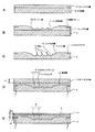
図12に、ウェットエッチング法を用いたマイクロレンズアレイ基板の製造方法を示す。先ず、図12Aに示すように、ガラスあるいは石英からなる基板31上にマイクロレンズアレイに対応するように複数の円形の開口32aを有したレジストマスク32を形成する。次に、図12Bに示すように、レジストマスク32を介してHF系エッチャントによる等方性エッチングを行い基板31の表面に複数のレンズ形状の凹部(球面状の凹部)33を形成する。次に、レジストマスク32を除去した後、図12Cに示すように、基板31上に基板と異なる屈折率の樹脂34を塗布し、樹脂34を凹部33内に充填する。この凹部33の樹脂34と基板31とによって複数のマイクロレンズ35が連続して配列されたマイクロレンズアレイ36が形成される。次いで、図12Dに示すように、樹脂34を介して基板31上にカバーガラス板37を貼り合わせ、所要の厚さまで研磨し、さらにカバーガラス板37上に例えばITO(酸化インジウム錫)の透明電極38を形成してマイクロレンズアレイ基板39を作製する。
FIG. 12 shows a method for manufacturing a microlens array substrate using a wet etching method. First, as shown in FIG. 12A, a
図13に、2P法を用いたマイクロレンズアレイ基板の製造方法を示す。先ず、図13Aに示す複数のマイクロレンズ形状42を配列してなるマイクロレンズアレイ形状43が一体に形成されたスタンパー41を用意する。次に、図13Bに示すように、ガラス基板44上に第1の樹脂層45を形成し、この樹脂層45にスタンパー41のマイクロレンズアレイ形状42を圧着する。次いで、図13Cに示すように、スタンパー41を剥離することにより、第1の樹脂層45の表面にマイクロレンズアレイ形状の凹部46が転写される。次に、図13Dに示すように、第1の樹脂層45上にこれとは屈折率の異なる第2の樹脂47を塗布し、第2の樹脂47を凹部46内に充填する。この第1の樹脂層45と第2の樹脂47により複数のマイクロレンズ48が配列されてなるマイクロレンズアレイ49が形成される。次いで、図13Eに示すように、第2の樹脂47を介してガラス基板44上にカバーガラス板50を貼り合わせ、カバーガラス板50を所要の厚さまで研磨する。その後、カバーガラス板50上に例えばITO(酸化インジウム錫)の透明電極51を形成してマイクロレンズアレイ基板52を作製する。
FIG. 13 shows a method of manufacturing a microlens array substrate using the 2P method. First, a
上述のウェットエッチング法を用いたマイクロレンズアレイ基板の製造方法については、特許文献1に記載されている。また、2P法を用いたマイクロレンズアレイ基板の製造方法については、特許文献2に記載されている。
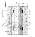
上述した石英基板またはガラス基板にマイクロレンズアレイ36が形成され、このマイクロレンズアレイ基板31に樹脂を充填してカバーガラス37を貼り合わせ、硬化したとき、図14に示すように、マイクロレンズアレイ36が形成された周縁部に気泡30が発生してしまう。この気泡30は、マイクロレンズアレイ36領域と周縁部での樹脂の収縮によるひずみの発生、及び樹脂厚の急激な変化が生じるために発生してしまう。2P法を用いたマイクロレンズアレイ基板の場合にも、同様にマイクロレンズアレイ領域周縁部において、第1の樹脂層と第2の樹脂層間に気泡が発生する。気泡が入らなくても、ひずみによってあたかも気泡が発生したように画面上に光って見えることがある。
When the
本発明は、上述の点に鑑み、樹脂を充填して硬化させるときに気泡が発生することなく、また、ひずみを低減するマイクロレンズアレイ基板を提供するものである。 In view of the above-described points, the present invention provides a microlens array substrate that does not generate bubbles when resin is filled and cured, and that reduces distortion.
本発明に係るマイクロレンズアレイ基板は、石英基板またはガラス基板の表面内に連続した複数のレンズ状凹部が形成され、前記レンズ状凹部内に樹脂が充填されてマイクロレンズアレイが形成され、前記石英基板またはガラス基板の前記マイクロレンズアレイ周縁部に対応する部分が、基板表面に向ってテーパー状に形成されているマイクロレンズアレイであることを特徴とする。 In the microlens array substrate according to the present invention, a plurality of continuous lens-shaped concave portions are formed in the surface of a quartz substrate or a glass substrate, and the lens-shaped concave portions are filled with a resin to form a microlens array. A portion of the substrate or glass substrate corresponding to the peripheral edge of the microlens array is a microlens array formed in a tapered shape toward the substrate surface.
本発明に係る好ましい形態としては、前記石英基板またはガラス基板の表面に、前記樹脂を挟んでカバーガラス部材が貼り合わされている。前記テーパーは、階段状に形成されることが好ましい。前記テーパーは、下に凸状の曲線で形成されることが好ましい。前記テーパーは、上に凸状の曲線で形成されることが好ましい。前記テーパーは、多重露光で形成されることが好ましい。 As a preferred embodiment according to the present invention, a cover glass member is bonded to the surface of the quartz substrate or the glass substrate with the resin interposed therebetween. The taper is preferably formed in a step shape. The taper is preferably formed with a downwardly convex curve. The taper is preferably formed as a convex curve upward. The taper is preferably formed by multiple exposure.
本発明に係るマイクロレンズアレイ基板によれば、マイクロレンズアレイ基板上のマイクロレンズアレイの周縁部に基板表面に向ってテーパー部を設けることで、樹脂を充填した後、カバーガラスを貼り合せて樹脂を硬化させたときに、マイクロレンズアレイと周縁部の収縮を緩和して気泡やひずみを発生させることなく良好なマイクロレンズアレイ基板を形成することができる。気泡が発生しないため、マイクロレンズアレイの最外周のマイクロレンズも利用することができる。 According to the microlens array substrate of the present invention, the resin is filled with a taper portion at the peripheral portion of the microlens array on the microlens array substrate toward the substrate surface, and then the cover glass is bonded to the resin. When the is cured, it is possible to relax the contraction of the microlens array and the peripheral portion and form a good microlens array substrate without generating bubbles or distortion. Since no bubbles are generated, the outermost microlens of the microlens array can also be used.
本発明に係るマイクロレンズアレイ基板によれば、石英基板またはガラス基板の表面内に連続した複数の凹レンズ状のマイクロレンズアレイが直接形成されるので、パターン寸法精度のよい精密なマイクロレンズアレイを有するマイクロレンズアレイ基板を提供することができる。このマイクロレンズアレイが、石英基板またはガラス板の表面に形成したレンズ状凹部内に屈折率の異なる樹脂層を充填して形成されるので、使用材料を少なくし構造を簡単化することができる。 According to the microlens array substrate according to the present invention, since a plurality of continuous concave lens-shaped microlens arrays are directly formed on the surface of the quartz substrate or the glass substrate, the microlens array substrate has a precise microlens array with good pattern dimensional accuracy. A microlens array substrate can be provided. Since this microlens array is formed by filling a resin layer having a different refractive index into a lens-shaped concave portion formed on the surface of a quartz substrate or a glass plate, the structure can be simplified with less material used.
また、隣り合うマイクロレンズ間の境界部分では、非レンズ領域がない状態で形成され、境界部分もレンズ領域として形成されるので、集光効率のよいマイクロレンズアレイ基板となる。マイクロレンズアレイが多重露光法を用いて形成されるので、レンズ曲面として球面状あるいは非球面状のものが得られ、目的に合ったレンズ曲面のマイクロレンズアレイ基板を提供することができる。レンズ状凹部内に、石英基板またはガラス基板より屈折率の大きい樹脂を充填することにより、ガラス基板側から入射した光はガラス基板と樹脂層の境界部で屈折し、集光レンズとしての機能を持たせる事ができる。 In addition, the boundary portion between adjacent microlenses is formed without a non-lens region, and the boundary portion is also formed as a lens region, so that a microlens array substrate with high light collection efficiency is obtained. Since the microlens array is formed by using the multiple exposure method, a spherical surface or an aspherical surface can be obtained as the lens curved surface, and a microlens array substrate having a lens curved surface suitable for the purpose can be provided. By filling the lens-shaped recess with a resin having a higher refractive index than that of the quartz substrate or the glass substrate, the light incident from the glass substrate side is refracted at the boundary between the glass substrate and the resin layer, and functions as a condensing lens. You can have it.
以下、図面を参照して本発明の実施の形態を説明する。
<第1実施の形態>
図1及び図2に、本発明に係るマイクロレンズアレイ基板およびその製造方法の一実施の形態を示す。本例は、液晶プロジェクタを構成する液晶パネル用のマイクロレンズアレイ基板について説明する。
先ず、図1Aに示すように、透明基板である平行平板の石英基板またはガラス基板、本例では石英基板2を用意する。この平行平板の石英基板の表面上に所要の厚さのフォトレジスト層3aを形成する。本例ではスピンコート法によりフォトレジスト層3aを形成する。
Embodiments of the present invention will be described below with reference to the drawings.
<First embodiment>
1 and 2 show an embodiment of a microlens array substrate and a manufacturing method thereof according to the present invention. In this example, a microlens array substrate for a liquid crystal panel constituting a liquid crystal projector will be described.
First, as shown in FIG. 1A, a parallel plate quartz substrate or glass substrate, which is a transparent substrate, in this example, a
次に、図1Bに示すように、フォトレジスト層3aに対してフォトリソグラフィー処理(パターン露光、現像処理)を行うことによって、表面にマイクロレンズアレイの原型となる連続した複数のマイクロレンズ形状の凹状曲面(以下、レンズ状凹部という)4と、マイクロレンズアレイの周縁部に対応する部分の表面に向って傾斜するテーパー状の領域(以下、テーパー部という)20と、表示領域(いわゆるマイクロレンズアレイとなるレンズ状凹部4の領域)の外側、すなわちテーパー部20の外側に位置したステッパ用のアライメントマークに対応した縦溝パターン5とを有したレジスト層3bを形成する。テーパー部20は、より正確にはマイクロレンズアレイとなるレンズ状凹部4の領域の最外周のレンズ状凹部4から表面に向って形成する。このフォトリソグラフィー処理は、例えば多重露光法を用いる。レンズ状凹部4では、図6に示すように、フォトレジスト層3aに対して、複数枚の露光マスク(多重マスク)61〔611、612、613、614、615〕を用いて順次パターン露光62〔621、622、623、624、625〕を行う。テーパー部20では、レンズ状凹部4の形成と同時に、図7に示すように、フォトレジスト層3aに対して複数枚の露光マスク(多重マスク)63[631、632、633、634]を用いて順次パターン露光64[641、642、643、644]を行う。この場合、レンズ状凹部4の露光マスク61とテーパー部20の露光マスク63は同一の露光マスクとして構成したものを用いることができる。露光量は、パターン露光621〜625の順に、また、パターン露光641〜644の順に多くなる。多重露光は、例えばi線ステッパ装置を用いて行うことができる。この多重露光後に現像処理が行われる。この多重露光法によって、レンズ状凹部4の曲面形状及びテーパー部20の形状を任意に制御することができ、目的のレンズ形状に合った例えば球面形状、非球面形状などの形成及びテーパー部20の形成が可能になる。
Next, as shown in FIG. 1B, a photolithographic process (pattern exposure, development process) is performed on the photoresist layer 3a, whereby a plurality of continuous microlens-shaped concave shapes that become the prototype of the microlens array are formed on the surface. A curved surface (hereinafter referred to as a lens-shaped concave portion) 4, a tapered region (hereinafter referred to as a tapered portion) 20 that is inclined toward the surface of a portion corresponding to the peripheral portion of the microlens array, and a display region (a so-called microlens array) A resist layer 3b having a vertical groove pattern 5 corresponding to an alignment mark for a stepper located outside the region of the lens-shaped concave portion 4), that is, outside the tapered portion 20, is formed. More specifically, the tapered portion 20 is formed from the lens-shaped
次に、図1Cに示すように、レジスト層3b上からの異方性エッチングによるドライエッチングにより、レジスト層3bの表面側に形成されたレンズ状凹部4、マイクロレンズアレイの周縁部に対応する部分の表面に向って傾斜するテーパー部20及び縦溝パターン5を、石英基板2の表面に転写する。このドライエッチングでは、レジスト層3bと石英基板2のエッチング選択比が同じになるエッチングガスが選ばれる。エッチングガスとしては、例えばCF4、CF3H、CH2H2、C3F8、SF6等のガスを用いることができる。このドライエッチングにより、最外周のレンズ状凹部6から石英基板2の表面にはマイクロレンズアレイとなる連続した複数のレンズ状凹部6、マイクロレンズアレイの周縁部に対応する部分を基板表面に向って傾斜するテーパー部21と、その外側に位置するステッパ用の縦溝状のアライメントマーク7が形成される。この場合、各レンズ状凹部6は、それぞれ曲面全面がレンズ形状に形成される。したがって隣り合うレンズ状凹部6の境界部分では、両曲面が突き合わされるように先鋭状の頂点18となる。
Next, as shown in FIG. 1C, a lens-
次に、図1Dに示すように、石英基板2の表面にレンズ状凹部6及びステッパ用のアライメントマーク7内に充填されるように石英基板2と屈折率が異なる樹脂層9を形成し、平坦化されている樹脂層9上に所要の厚さd1の平行平板のカバーガラス板10を貼り合わせる。ここでの樹脂層9としては、石英基板2の屈折率より大きい屈折率を有する樹脂を用いる。樹脂層9としては、例えばエピスルフィド系、その他エポキシ系、アクリル系の樹脂を用いることができる。本例では、石英基板2の表面に例えば熱硬化性の樹脂9を注入し、すなわち滴下しカバーガラス板10を載置した状態で、スピン回転させて樹脂9をレンズ状凹部6、テーパー部21及びアライメントマーク7内に充填させる。その後、熱硬化処理でカバーガラス板10が石英基板2に貼り合わされる。この熱硬化処理のときに、石英基板2のマイクロレンズアレイの周縁部に対応する部分にテーパー部が設けられていることにより、マイクロレンズアレイ8の周縁部に気泡を発生させずに樹脂を硬化させることができる。石英基板2とそのレンズ状凹部6に充填された樹脂層9とによって複数のマイクロレンズ11が連続して配列されたマイクロレンズアレイ8を形成する。このマイクロレンズアレイ8を構成する連続したマイクロレンズ11は、隣り合うマイクロレンズ11の境界部分に非レンズ領域のない連続したマイクロレンズとなる。同時にこのマイクロレンズアレイ領域の外側に縦溝状パターン5に樹脂層9が充填されたアライメントマーク7が形成される。
Next, as shown in FIG. 1D, a
次に、図1Eに示すように、カバーガラス板10を研磨して凹状のマイクロレンズの頂点からカバーガラス表面までのカバー表層厚d2を薄くする。このカバー表層厚d2としては、5μm以上30μm以下、好ましくは20μm未満、より好ましくは10μm以下の厚さとすることができる。また、マイクロレンズの頂点からカバーガラス裏面までの樹脂層9の厚さd3としては、1μm以上10μm以下の厚さとすることができる。このときの樹脂の粘度としては、1cp以上100cp以下であればよく、本例では30cp程度の粘度の樹脂を用いる。
Next, as shown in FIG. 1E, the
ここで、カバー表層厚d2が30μmを越えると、高解像度化に伴なってマイクロレンズ11を微細化していったときに、マイクロレンズ11の焦点深度を目的の位置に合わせることができず、集光効率が低下する。d2が20μm未満、10μm以下と薄くして行くにしたがい、マイクロレンズの更なる微細化を可能にする。カバー表層厚d2は、基板面内の厚さd2のばらつき発生を考慮すると、5μmが製造可能な下限である。一方、樹脂層9の厚さd3は限りなく薄くすることが望まれるが、マイクロレンズを再現性よく作るには1μmが下限となる。厚さd3が10μmを越えると、カバー表層厚d2に影響し、液晶パネル等に適用したときの高解像度化を困難にする。
Here, when the cover surface layer thickness d2 exceeds 30 μm, when the
次に、図2Fに示すように、カバーガラス板10上にいわゆるブラックマトリックスとなる金属膜等からなる遮光膜、本例ではアルミニウム(Al)膜13を蒸着またはスパッタ等により成膜する。
Next, as shown in FIG. 2F, a light shielding film made of a metal film or the like that becomes a so-called black matrix, in this example, an aluminum (Al)
次に、図2Gに示すように、石英基板2に形成したアライメントマーク7を読み取ることが出来るように、アライメントマーク7に対応する部分のアルミニウム膜13を選択エッチングにより除去し、開口(いわゆるマーカー窓)14を形成する。開口14の形成はラフな精度で形成することができる。
Next, as shown in FIG. 2G, a portion of the
次に、図2Hに示すように、アライメントマーク7を基準にi線ステッパ装置の露光マスクとの位置合わせを行い、リソグラフィ技術を用いてアルミニウム膜13を選択エッチングによりパターニングしてブラックマトリックス15を形成する。このブラックマトリックス15は、図9に示すように、連続する各マイクロレンズ11の境界部分を残すように格子状のパターンに形成する。この場合、アライメントマーク7が石英基板2に形成されているので、アライメントマーク7の位置が高精度に得られるため、マイクロレンズ11を例えば一辺10μmの略四角形状としたとき、ブラックマトリックス15は±1μm程度の位置合わせ精度で形成することができる。このブラックマトリックス15のパターン時に、同時にアルミニウム膜13によるアライメントマーク、すなわち後述する液晶パネルを構成する画素電極及び薄膜トランジスタ(TFT)が形成されたいわゆるTFT基板の貼り合わせ用のアライメントマーク16を形成する。
Next, as shown in FIG. 2H, alignment with the exposure mask of the i-line stepper apparatus is performed with reference to the
次に、図2Iに示すように、ブラックマトリックス15及びアライメントマーク16が形成されたカバーガラス板10上に透明導電膜、例えばITO(酸化インジウム錫)膜による対向電極17を成膜して目的の平行平板のマイクロレンズアレイ基板1を得る。なお、本実施の形態におけるマイクロレンズアレイ基板1の画素ピッチは10μm×10μmの高精細なものである。
Next, as shown in FIG. 2I, a counter electrode 17 made of a transparent conductive film, for example, an ITO (indium tin oxide) film is formed on the
上述の本実施の形態に係るマイクロレンズアレイ基板1によれば、石英基板2の表面に直接レンズ状凹部6をドライエッチングによる転写法で形成し、このレンズ状凹部内に樹脂を充填することによって、連続して配列された複数のマイクロレンズ11からなるマイクロレンズアレイ8が石英基板2の表面内に直接構成される。この構成では、石英基板の表面内の直接マイクロレンズアレイ8が形成されているので、パターン寸法精度のよい精密なマイクロレンズアレイ8を有するマイクロレンズアレイ基板1を提供することができる。
According to the
また、隣り合うマイクロレンズ11間の境界部分では、非レンズ領域がない状態で形成されている。すなわち、レンズ状凹部6が石英基板2に形成されているので、境界部分がだれることなく先鋭な頂点18として形成され、境界部分もレンズ領域として形成されることになる。従って、集光効率のよいマイクロレンズアレイ基板となる。
マイクロレンズアレイ8が多重露光法を用いて形成されるので、レンズ曲面として球面状あるいは非球面状のものが得られ、目的に合ったレンズ曲面のマイクロレンズアレイ基板を提供することができる。
Further, the boundary portion between the
Since the
一方、石英基板2のマイクロレンズアレイ8の周縁部に対応する部分に、最外周のマイクロレンズ11から基板表面に向って傾斜するテーパー部21を設けることで、樹脂9を充填した後、カバーガラス10を貼り合せて樹脂を硬化させたときに、マイクロレンズアレイ8と周縁部の収縮を緩和して気泡やひずみを発生させることなく良好なマイクロレンズアレイ基板1を形成することができる。気泡が発生しないため、マイクロレンズアレイ8の最外周のマイクロレンズ11も利用することができる。
On the other hand, a taper portion 21 inclined from the
石英基板2にレンズ状凹部6と共に、ステッパ用のアライメントマーク7を一体に有するので、位置精度のよいアライメントマーク7が得られる。また、別工程で形成する必要がなく、製造工程の簡素化が図れる。
マイクロレンズアレイ8が形成された表面側に所要の薄い厚さのカバーガラス板10が形成され、このカバーガラス板10表面には隣り合うマイクロレンズ11の境界部分に一致した位置にブラックマトリックス15が形成されていることにより、ブラックマトリックス15はマイクロレンズ11に最も近い位置に形成されることになる。このようなブラックマトリックス15を有することにより、液晶パネルを構成したときに、隣り合うマイクロレンズ11間の境界部分の先鋭な頂点に光が照射され、迷光成分が発生したとしても、ブラックマトリックス15によって迷光成分のTFT回路側へ入射することを確実に阻止することができる。
カバー表層厚d2を5μm以上30μm以下、さらに樹脂厚d3を1μm以上5μm以下に薄くすることにより、高解像度化に伴ってマイクロレンズ11が微細化した場合にも、光を目的の領域に集光させることができる。すなわち、微細化したマイクロレンズ11のレンズ焦点深度を目的の領域に合わせることができる。つまり、光路設計の自由度が上がる。
Since the
A
The cover surface layer thickness d2 is reduced to 5 μm or more and 30 μm or less, and the resin thickness d3 is reduced to 1 μm or more and 5 μm or less. Can be made. That is, the lens focal depth of the
本実施の形態に係るマイクロレンズアレイ基板の製造方法によれば、石英基板2の表面にドライエッチングによってレジスト層3bのレンズ状凹部4を転写して、レンズ状凹部6を形成し、このレンズ状凹部6内の樹脂層9を充填してマイクロレンズアレイ8を形成している。石英基板2自身は樹脂層のように収縮が起こらず、パターン寸法精度の良いマイクロレンズアレイ8を形成することができる。また、石英基板2に直接レンズ状凹部6を転写するので、隣り合うマイクロレンズ11間のレンズ境界部分がレンズ領域として使える。すなわち、レンズ状凹部6も隣り合うマイクロレンズとの境界部分でだれる等の変形が起こらないので、非レンズ領域のないマイクロレンズアレイ8を形成することができる。従って、集光効率の良いマイクロレンズアレイ8を形成することができる。
According to the method for manufacturing a microlens array substrate according to the present embodiment, the lens-shaped recess 6 is formed by transferring the lens-shaped
フォトレジスト層3aの表面にレンズ状凹部4を形成するめの露光として、多重露光法を用いることにより、レンズ状凹部4の曲面形状を任意に制御するもとができる。すなわち、マイクロレンズアレイ8のレンズ曲面やレンズ深さを自由自在に任意に設計することができ、石英基板2の表面に目的に合わせて球面状あるいは非球面状のレンズ状凹部6を形成することができる。従って、レンズ形状の制御性に優れる。
As the exposure for forming the lens-shaped
多重露光法と転写を用いて石英基板2のマイクロレンズアレイ8の周縁部に対応する表面に最外周のレンズ状凹部6から連続して基板表面に向って傾斜するテーパー部21を形成することにより、その後に樹脂9を充填し、カバーガラス10を貼り合せて樹脂を硬化させたときに、マイクロレンズアレイ8と周縁部の収縮を緩和することができ、気泡やひずみを発生させることなく良好なマイクロレンズアレイ基板1を形成することができる。気泡が発生しないため、マイクロレンズアレイの最外周のマイクロレンズも利用することができる。
By using a multiple exposure method and transfer, a tapered portion 21 is formed on the surface of the
石英基板2の表面にレンズ状凹部6の転写と同時に、ステッパ用のアライメントマーク7を形成するので、位置精度の良いアライメントマーク7を形成することができ、ステッパ装置のマスク合わせを精度良く行える。これにより、ブラックマトリックス15を隣り合うマイクロレンズ11間の境界に対応した部分に精密に形成することができる。また、アライメントマークの形成工程を別途必要とせず、工程の簡素化を図ることができる。
Since the
カバーガラス板10として、カバー表層厚d2を5μm以上30μm以下、さらに樹脂厚d3を1μm以上10μm以下に薄く形成することができるので、高解像度化に伴ってマイクロレンズ11を微細化した場合にも、焦点深度に合わせてカバーガラス板10を薄くすることが可能になり、高解像度に対応したマイクロレンズアレイ基板1を製造することができる。
The
マイクロレンズアレイ基板1において、マイクロレンズアレイ8に最も近いカバーガラス板10表面にブラックマトリックス15を一体に形成している。しかも、ブラックマトリックス15は、連続するレンズ状凹部6の頂点18に合わせるように形成する。これによって、液晶パネルを構成したときに、隣り合うマイクロレンズ11間の境界部分の先鋭な頂点18に入射した光により迷光成分が発生しても、TFT回路側への入射を確実に阻止することがきる。
In the
樹脂層としては1種類の樹脂層9だけを使用するので、耐熱性、耐光性に優れる。石英基板2のレンズ状凹部6に樹脂層9を充填してマイクロレンズアレイ8を形成するので、使用材料が少なく、工程数も少なくなり、構造の簡単なマイクロレンズアレイ基板1を製造することができる。
Since only one type of
因みに、前述した従来の図13で示すような2P法を用いたマイクロレンズアレイ基板の製造方法では、スタンパー41でレンズ形状を樹脂層45に転写するため、量産性に優れている。しかし、樹脂層45の硬化時の熱収縮によりマイクロレンズアレイのパターン寸法に制御が難しい。また、樹脂層45に凹部46を形成するため、隣り合う凹部46の境界部分、すなわち頂部53(図13参照)では鋭角を維持できずに丸みを帯びてしまい、結果として境界部分が非レンズ領域となってしまう。特に高解像度化のためにマイクロレンズ自体を微細化していった場合、この非レンズ領域に割合が増えることになり、マイクロレンズアレイの形成が困難となる。また、2種類の樹脂を用いるので、耐熱性、耐光性に限界があった。さらに、前述の図12に示すような、ウェットエッチング法を用いたマイクロレンズアレイ基板の製造方法では、等方エッチングであることから、マイクロレンズの形状が球面状にしかならず、他の非球面形状のマイクロレンズを形成することができない。すなわち、レンズ形状の制御性がない。一方、従来ではカバー表層厚すなわち凹部状レンズの頂点部の樹脂層からカバーガラス板の表層までの厚みは30μmが限界で、これより薄く形成できなかった。その理由は、樹脂層を形成するときの樹脂の粘度(実際は粘度が100cpより高い粘度の樹脂を用いた)の影響で樹脂層が薄く形成できないためであった。これに対して、本実施の形態では上述したようにこのような従来の問題点を解決することができる。
Incidentally, in the conventional method for manufacturing a microlens array substrate using the 2P method as shown in FIG. 13, since the lens shape is transferred to the
上述の本実施の形態に係るマイクロレンズアレイ基板の製造方法では、多重露光法を適用したが、フォトリソグラフィー技術によるパターン露光としては、多重露光法に変えて1枚のマスクにおいてレンズ形状に合わせて光透過率を中央から周辺に向かって変化させた、いわゆるグレーマスクを用いて露光するグレーマスク法で行ってもよい。 In the manufacturing method of the microlens array substrate according to the above-described embodiment, the multiple exposure method is applied. However, as the pattern exposure by the photolithography technique, the multiple exposure method is used in accordance with the lens shape in one mask. You may carry out by the gray mask method of exposing using what is called a gray mask which changed the light transmittance toward the periphery from the center.
<第2実施の形態>
次に、図3〜図4に、本発明に係るマイクロレンズアレイ基板及びその製造方法の他の実施の形態を示す。本例も、液晶プロジェクタを構成する液晶パネル用のマイクロレンズアレイ基板に適用した場合である。
本実施の形態においては、図3Aから図3Cまでの工程は、前述の図1Aから図1Cまでの工程と同じであるので、重複説明を省略する。
<Second Embodiment>
Next, FIGS. 3 to 4 show other embodiments of the microlens array substrate and the manufacturing method thereof according to the present invention. This example is also a case where the present invention is applied to a microlens array substrate for a liquid crystal panel constituting a liquid crystal projector.
In the present embodiment, the steps from FIG. 3A to FIG. 3C are the same as the steps from FIG. 1A to FIG.
本実施の形態では、図3Cの工程の後、図3Dに示すように、石英基板2の表面にTFT基板貼り合わせ用のアライメントマーク16を形成する。例えば、前述と同じように例えばアルミニウム膜を石英基板2の表面全面に成膜し、ステッパ用のアライメントマーク7に対応した部分にアルミニウム膜を選択的にエッチング除去して開口を形成する。次いで、アライメントマーク7を基準にi線ステッパ装置の露光マスクとの置合わせを行い、リソグラフィ技術を用いてアルミニウム膜を選択エッチングによりパターニングしてアライメントマーク16を形成する。
In the present embodiment, after the step of FIG. 3C, as shown in FIG. 3D, an
次に、図4Eに示すように、石英基板2の表面にレンズ状凹部6、テーパー部21及びステッパ用のアライメントマーク7内に充填されるように石英基板2と屈折率が異なる樹脂層9を形成し、平坦化されている樹脂層9上に所要の厚さd1の平行平板のカバーガラス板10を貼り合わせる。ここでの樹脂層9としては、石英基板2の屈折率より大きい屈折率を有する樹脂を用いる。本例では、石英基板2の表面に例えば熱硬化性の樹脂9を滴下しカバーガラス板10を載置した状態で、スピン回転させて樹脂9をレンズ状凹部6及びアライメントマーク7内に充填させる。その後、熱硬化処理でカバーガラス板10が石英基板2に貼り合わされる。石英基板2とそのレンズ状凹部6に充填された樹脂層9とによって複数のマイクロレンズ11が連続して配列されたマイクロレンズアレイ8を形成する。このマイクロレンズアレイ8を構成する連続したマイクロレンズ11は、隣り合うマイクロレンズ11の境界部分に非レンズ領域のない連続したマイクロレンズとなる。同時にこのマイクロレンズアレイ領域の外側に縦溝状パターン5に樹脂層9が充填されたアライメントマーク7が形成される。
Next, as shown in FIG. 4E, a
次に、図4Fに示すように、カバーガラス板10を研磨してマイクロレンズの頂点からカバーガラス表面までのカバー表層厚d2を薄くする。前述と同様に、このカバー表層厚d2としては、5μm以上30μm以下、好ましくは20μm未満、より好ましくは10μm以下の厚さとすることができる。また、樹脂層9の厚さd3としては、1μm以上10μm以下の厚さとすることができる。樹脂の粘度としては、1cp以上100cp以下であればよく、本例では30cpの粘度の樹脂を用いる。
Next, as shown in FIG. 4F, the
次に、図4Gに示すように、カバーガラス板10上に透明導電膜、例えばITO(酸化インジウム錫)膜による対向電極17を成膜して目的のマイクロレンズアレイ基板71を得る。
Next, as shown in FIG. 4G, a counter electrode 17 made of a transparent conductive film, for example, an ITO (indium tin oxide) film is formed on the
本実施の形態に係るマイクロレンズアレイ基板71及びその製造方法では、カバーガラス板10上にブラックマトリックスを形成しない点を除く、その他の構成及び製造方法は、前述のマイクロレンズアレイ基板1と同様である。従って、本実施の形態に係るマイクロレンズアレイ基板71及びその製造方法においても、ブラックマトリックスの効果を除いて、前述したマイクロレンズアレイ基板1と同様の効果を奏する。
In the microlens array substrate 71 and the manufacturing method thereof according to the present embodiment, other configurations and manufacturing methods are the same as those of the
<第3実施の形態>
図5に、本発明に係るマイクロレンズアレイ基板81の第3の実施の形態を示す。
本例も、液晶プロジェクタを構成する液晶パネル用のマイクロレンズアレイ基板に適用した場合である。
本実施の形態においては、図1Aから図2Hまでの工程は同じであるので、重複説明は省略する。
<Third Embodiment>
FIG. 5 shows a third embodiment of a microlens array substrate 81 according to the present invention.
This example is also a case where the present invention is applied to a microlens array substrate for a liquid crystal panel constituting a liquid crystal projector.
In the present embodiment, the steps from FIG. 1A to FIG. 2H are the same, and thus a duplicate description is omitted.
本実施の形態では、図2Hの工程の後、図5に示すように、ブラックマトリックス15及びアライメントマーク16が形成されたカバーガラス板10上に透明保護層、例えばシリコン酸化膜(SiO2膜)19を成膜し、さらに上層に透明導電膜、例えばITO(酸化インジウム錫)膜による対向電極17を成膜して目的の平行平板のマイクロレンズアレイ基板81を得る。
In the present embodiment, after the step of FIG. 2H, as shown in FIG. 5, a transparent protective layer such as a silicon oxide film (
本実施の形態に係るマイクロレンズアレイ基板及びその製造方法では、ブラックマトリックス15及びアライメントマーク16が形成されたカバーガラス板10上にシリコン酸化膜19を成膜している点を除いて、その他の構成及び製造方法は、前述のマイクロレンズアレイ基板1と同様である。本実施の形態によれば、例えば、Alで成膜したブラックマトリックス15及びアライメントマーク16をシリコン酸化膜19で覆うことにより、Alの酸化を防ぐことができ、長期に渡りブラックマトリックス15として使用することができる。また、透明保護層となるシリコン酸化膜19が反射防止膜として作用し、光透過率を上げることができ、集光効率を向上することができる。その他、本実施の形態に係るマイクロレンズアレイ基板及びその製造方法においても、前述したマイクロレンズアレイ基板1と同様の効果を奏する。
In the microlens array substrate and the manufacturing method thereof according to the present embodiment, except that the silicon oxide film 19 is formed on the
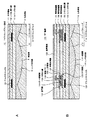
図8に、本発明に係るマイクロレンズアレイ基板の石英基板またはガラス基板に形成するテーパー部21の具体例を示す。 FIG. 8 shows a specific example of the tapered portion 21 formed on the quartz substrate or the glass substrate of the microlens array substrate according to the present invention.
図8Aに示すテーパー部211は、なだらかな直線的な傾斜状のテーパーである。 A tapered portion 211 shown in FIG. 8A is a gentle linearly inclined taper.
図8Bに示すテーパー部212は、基板表面に向って階段状のテーパーである。この階段状のテーパーは、樹脂を充填した後、熱硬化しても気泡を発生させない段数に形成する必要がある。 The tapered portion 212 shown in FIG. 8B is a stepped taper toward the substrate surface. The step-like taper needs to be formed in a number of steps that does not generate bubbles even after thermosetting after filling with resin.
図8Cに示すテーパー部213は、基板表面に向って上に凸状のテーパーである。 The tapered portion 213 shown in FIG. 8C is a taper convex upward toward the substrate surface.
図8Dに示すテーパー部214は、基板表面に向って下に凸状のテーパーである。 The tapered portion 214 shown in FIG. 8D is a taper convex downward toward the substrate surface.
テーパー部の形状は、樹脂を充填した後、熱硬化のとき熱収縮により気泡が発生しない形状に形成すればよいので、特に上記形状に限らない。 The shape of the taper portion is not particularly limited to the above-mentioned shape because it may be formed in a shape in which bubbles are not generated due to thermal shrinkage after thermosetting after filling with resin.
次に、図10及び図11を参照して上述したマイクロレンズアレイ基板81を用いて製造した液晶プロジェクタ用の液晶パネルを説明する。
図10Aに示すように、前述の図5で得られたマイクロレンズアレイ基板81を、図示せざるも分割線より分割して各液晶パネルに対応したマイクロレンズアレイ基板101を形成する。すなわち、表面側のレンズ状凹部6に樹脂層9を充填して連続した複数のマイクロレンズ11からなるマイクロレンズアレイ8を形成した石英基板2上に、カバーガラス板10を貼り合わせ、カバーガラス板10上に格子状のブラックマトリックス15を形成し、さらに透明保護層であるシリコン酸化膜19と対向電極17を形成したマイクロレンズアレイ基板101を用意する。
Next, a liquid crystal panel for a liquid crystal projector manufactured using the microlens array substrate 81 described above with reference to FIGS. 10 and 11 will be described.
As shown in FIG. 10A, the microlens array substrate 81 obtained in FIG. 5 is divided by a dividing line (not shown) to form a microlens array substrate 101 corresponding to each liquid crystal panel. That is, the
一方、図10Bに示すように、同様の製法を用いてマイクロレンズアレイを形成した透明基板上に薄膜トランジスタ(TFT)及び画素電極を形成したTFT基板102を形成する。すなわち、透明基板である例えば石英基板またはガラス基板、本例では石英基板112に、前述の図1A〜図1Eと同様の工程を用いてレンズ状凹部116に石英基板112と屈折率の異なる樹脂層119を充填して連続した複数のマイクロレンズ117からなるマイクロレンズアレイ118を形成する。また、樹脂層119上に所要の厚さに研磨されたカバーガラス板120を貼り合わせる。このカバーガラス板120上に各マイクロレンズ117を囲むように、すなわち各画素領域の周縁に沿って前述の図2Hで説明したと同様の遮光膜となる格子状のブラックマトリックス121を形成する。次いで、このブラックマトリックス121を埋め込む状態でカバーガラス板120上に透明保護層であるシリコン酸化膜122を形成した後、層間絶縁膜126の表面を例えばCMP(化学機械研磨)法により平坦化する。次に、多結晶シリコンからなる半導体薄膜123を選択的に形成する。この半導体薄膜123にSiイオンを注入してアモルファス化した後、熱処理して固相成長させて多結晶化する。
On the other hand, as shown in FIG. 10B, a thin film transistor (TFT) and a TFT substrate 102 on which pixel electrodes are formed are formed on a transparent substrate on which a microlens array is formed using the same manufacturing method. That is, a resin layer having a refractive index different from that of the
次に、半導体薄膜123上にゲート絶縁膜124を介して及びキャパシタの上部電極125を形成する。次いで、層間絶縁膜126を形成した後、半導体薄膜123の一方のソース・ドレイン領域に接続する信号線127を形成し、他方のソース・ドレイン領域に引き出し線128を形成する。次いで、層間絶縁膜129を形成し、引き出し線128に接続する配線パターン130を形成する。さらに層間絶縁膜131を形成し、この層間絶縁膜131上に下層の配線パターン130に接続する画素電極132を形成する。上記各層間絶縁膜126、129、131は、例えばシリコン酸化膜などで形成することができる。このように画素電極132を駆動する薄膜トランジスタ(TFT)回路133が設けられたTFT基板102を作製する。
Next, a capacitor
そして、図11に示すように、マイクロレンズアレイ基板101とTFT基板102を、前述したマイクロレンズアレイ基板101側に形成したアライメントマーク16(図2H参照)を基準に位置合わせして、所要の空間を挟んで対向配置し、空間内に液晶135を注入して封止し、液晶パネル140を作製する。この液晶パネル140は、両基板101及び102にマイクロレンズアレイ8及び118を有する、いわゆるダブルマイクロレンズ構造の液晶パネルでる。なお、図示せざるも、マイクロレンズアレイ基板102の対向電極17の表面、及びTFT基板102の画素電極132側の表面には、それぞれ配向膜を形成する。
Then, as shown in FIG. 11, the microlens array substrate 101 and the TFT substrate 102 are aligned with respect to the alignment mark 16 (see FIG. 2H) formed on the microlens array substrate 101 side as described above to obtain a required space. A liquid crystal panel 140 is manufactured by injecting the liquid crystal 135 into the space and sealing it. The liquid crystal panel 140 is a so-called double microlens liquid crystal panel having
この液晶パネル140によれば、マイクロレンズアレイ基板101及びTFT基板102のそれぞれのマイクロレンズアレイ8及び118が、石英基板2及び112の表面にドライエッチングによる転写法で直接形成されるので、精度のよい精密なマイクロレンズアレイを有することになる。しかも、石英基板2及び112に転写法でレンズ状凹部を形成するので、隣り合うマイクロレンズ11間の境界部分及び隣り合うマイクロレンズ間の境界部分、即ちそれぞれの頂点部分がだれることなく、レンズ領域と形成される。すなわち非レンズ領域のないマイクロレンズアレイ8及び118が形成される。この精度の良いマイクロレンズアレイ8及び118を有することによって、効率よく光を各画素へ集光することができる。また、マイクロレンズアレイ基板の石英基板2において、最外周のマイクロレンズ11から連続して基板表面に向ってテーパー部21が形成されるので気泡またはひずみの発生がなく、画質の向上が図れる。また、マイクロレンズアレイ基板102側に各マイクロレンズ11の境界部分に対応した位置にブラックマトリックス15が形成されるので、入射光が境界部分、すなわちレンズのエッジ部に照射され迷光成分が発生しても、この迷光成分がブラックマトリックス15により遮光され、TFT回路133側への入射を阻止できる。これによって、光リーク電流の発生や、フリッカやコントラストの低下などの画質上の不具合を防止することができる。
According to the liquid crystal panel 140, the
本実施の形態の液晶パネル140は、上述のマイクロレンズアレイ基板101を用いるので、高解像度化のためにマイクロレンズ自体を微細化していった場合にも、マイクロレンズアレイとして非レンズ領域がないので、マイクロレンズアレイとして有効に作用し、集光効率を上げることが可能になる。また、カバー表層厚が5μm以上30μm以下、樹脂層の厚さを1μm以上10μm以下と薄くすることにより、焦点距離を短くした微細なマイクロレンズの形成することができる。よって、高解像度でかつ信頼性の高い液晶プロジェクタ用の液晶パネルを提供することができる。 Since the liquid crystal panel 140 of the present embodiment uses the above-described microlens array substrate 101, even when the microlens itself is miniaturized for high resolution, there is no non-lens area as the microlens array. This effectively acts as a microlens array, and can improve the light collection efficiency. Further, by making the cover surface layer thickness as thin as 5 μm or more and 30 μm or less and the resin layer thickness as 1 μm or more and 10 μm or less, it is possible to form a micro lens having a short focal length. Therefore, a liquid crystal panel for a liquid crystal projector with high resolution and high reliability can be provided.
上例の液晶パネルでは、マイクロレンズアレイ基板81を用いたが、図2Iのマイクロレンズアレイ基板1を用いて構成することができる。また、マイクロレンズアレイ基板71を用いて構成することができる。この場合には、図11における層間絶縁膜129上に配線パターン130を挟んでTFT回路133への光入射を阻止するための遮光膜となるブラックマトリックスを形成する。
また、TFT基板として、マイクロレンズアレイ118を省略した構成のTFT基板を用いて、本発明のマイクロレンズアレイ基板との組み合わせで液晶パネルを構成することもできる。
Although the microlens array substrate 81 is used in the liquid crystal panel in the above example, the microlens array substrate 81 shown in FIG. 2I can be used. Further, the micro lens array substrate 71 can be used. In this case, a black matrix serving as a light shielding film for preventing light from entering the
Moreover, a liquid crystal panel can also be comprised by combining with the micro lens array substrate of this invention using the TFT substrate of the structure which abbreviate | omitted the
上例では、本発明に係るマイクロレンズアレイ基板を液晶パネルに適用したが、その他、輝度向上、あるいは視野角拡大のために、プラズマディスプレイ(PDP)、有機ELモニタ、フィールドエミッション(FPD)等の表示装置にもレンズアレイの屈折率や形状を変えることで用いることができる。さらに、本発明のマイクロレンズアレイ基板を照明装置に適用することも可能である。 In the above example, the microlens array substrate according to the present invention is applied to a liquid crystal panel. However, in order to improve the luminance or expand the viewing angle, plasma display (PDP), organic EL monitor, field emission (FPD), etc. The display device can also be used by changing the refractive index and shape of the lens array. Furthermore, the microlens array substrate of the present invention can be applied to a lighting device.
1・・マイクロレンズアレイ基板、2・・石英基板、3a・・フォトレジスト層、3b・・レジスト層、4・・レンズ状凹部、5・・縦溝パターン、6・・レンズ状凹部、7・・アライメントマーク、8・・マイクロレンズアレイ、9・・樹脂層、10・・カバーガラス板、11・・マイクロレンズ、13・・アルミニウム膜、14・・開口、15・・ブラックマトリックス、16・・アライメントマーク、17・・対向電極、18・・先鋭状の頂点、21[211、212、213、214]・・テーパー部、30・・気泡、31・・基板、32・・レジストマスク、32a・・開口、33・・凹部、34・・樹脂、35・・マイクロレンズ、36・・マイクロレンズアレイ、37・・カバーガラス板、38・・透明電極、39・・マイクロレンズアレイ基板、41・・スタンパー、42・・マイクロレンズ形状、43・・マイクロレンズアレイ形状、44・・ガラス基板、45・・第1の樹脂層、46・・凹部、47・・第2の樹脂、48・・複数のマイクロレンズ、49・・マイクロレンズアレイ、50・・カバーガラス板、51・・透明電極、52・・マイクロレンズアレイ基板、61〔611、612、613、614、615〕・・露光マスク(多重マスク)、62〔621、622、623、624、625〕・・パターン露光、63[631、632、633、634]・・露光マスク、64[641、642、643、644]・・パターン露光、71,81・・マイクロレンズアレイ基板、102・・TFT基板、112・・石英基板、116・・レンズ状凹部、117・・マイクロレンズ、118・・マイクロレンズアレイ、119・・樹脂層、120・・カバーガラス板、121・・ブラックマトリックス、122・・シリコン酸化膜、123・・半導体薄膜、124・・ゲート絶縁膜、125・・上部電極、126・・層間絶縁膜、127・・信号線、128・・引き出し線、129・・層間絶縁膜、130・・配線パターン、131・・層間絶縁膜、132・・画素電極、133・・薄膜トランジスタ(TFT)回路、140・・液晶パネル、
1 .. Microlens array substrate, 2 .. Quartz substrate, 3a .. Photoresist layer, 3b .. Resist layer, 4 .. Lens-shaped recess, 5 .. Vertical groove pattern, 6 .. Lens-shaped recess, 7 Alignment mark, 8 ... Micro lens array, 9 ... Resin layer, 10 ... Cover glass plate, 11 ... Micro lens, 13 ... Aluminum film, 14 ... Opening, ... 15 Black matrix, 16 ... Alignment mark 17 ..
Claims (6)
前記レンズ状凹部内に樹脂が充填されてマイクロレンズアレイが形成され、
前記石英基板またはガラス基板の前記マイクロレンズアレイ周縁部に対応する部分が、
基板表面に向ってテーパー状に形成されている
ことを特徴とするマイクロレンズアレイ基板。 A plurality of continuous lens-shaped recesses are formed in the surface of the quartz substrate or glass substrate,
The lens-shaped recess is filled with resin to form a microlens array,
The part corresponding to the microlens array peripheral part of the quartz substrate or the glass substrate,
A microlens array substrate characterized by being formed in a tapered shape toward the substrate surface.
ことを特徴とする請求項1記載のマイクロレンズアレイ基板。 The microlens array substrate according to claim 1, wherein a cover glass member is bonded to the surface of the quartz substrate or the glass substrate with the resin interposed therebetween.
ことを特徴とする請求項1記載のマイクロレンズアレイ基板。 The microlens array substrate according to claim 1, wherein the taper is formed in a step shape.
ことを特徴とする請求項1記載のマイクロレンズアレイ基板。 The microlens array substrate according to claim 1, wherein the taper is formed as a downwardly convex curve.
ことを特徴とする請求項1記載のマイクロレンズアレイ基板。 The microlens array substrate according to claim 1, wherein the taper is formed by an upwardly convex curve.
ことを特徴とする請求項1記載のマイクロレンズアレイ基板。 The microlens array substrate according to claim 1, wherein the taper is formed by multiple exposure.
Priority Applications (5)
| Application Number | Priority Date | Filing Date | Title |
|---|---|---|---|
| JP2004109161A JP4496824B2 (en) | 2004-04-01 | 2004-04-01 | Microlens array substrate, TFT substrate, liquid crystal panel, liquid crystal projector, display device, illumination device, and manufacturing method of microlens array substrate |
| US10/557,803 US7715104B2 (en) | 2004-03-26 | 2005-03-25 | Micro-lens array substrate and production method therefor |
| PCT/JP2005/006446 WO2005093466A1 (en) | 2004-03-26 | 2005-03-25 | Microlens array substrate and production method therefor |
| TW094109519A TW200603145A (en) | 2004-03-26 | 2005-03-25 | Microlens array substrate and production method therefor |
| US12/432,803 US7978413B2 (en) | 2004-03-26 | 2009-04-30 | Micro-lens array substrate and method for manufacturing thereof |
Applications Claiming Priority (1)
| Application Number | Priority Date | Filing Date | Title |
|---|---|---|---|
| JP2004109161A JP4496824B2 (en) | 2004-04-01 | 2004-04-01 | Microlens array substrate, TFT substrate, liquid crystal panel, liquid crystal projector, display device, illumination device, and manufacturing method of microlens array substrate |
Publications (2)
| Publication Number | Publication Date |
|---|---|
| JP2005292583A true JP2005292583A (en) | 2005-10-20 |
| JP4496824B2 JP4496824B2 (en) | 2010-07-07 |
Family
ID=35325550
Family Applications (1)
| Application Number | Title | Priority Date | Filing Date |
|---|---|---|---|
| JP2004109161A Expired - Fee Related JP4496824B2 (en) | 2004-03-26 | 2004-04-01 | Microlens array substrate, TFT substrate, liquid crystal panel, liquid crystal projector, display device, illumination device, and manufacturing method of microlens array substrate |
Country Status (1)
| Country | Link |
|---|---|
| JP (1) | JP4496824B2 (en) |
Cited By (4)
| Publication number | Priority date | Publication date | Assignee | Title |
|---|---|---|---|---|
| JP2007322503A (en) * | 2006-05-30 | 2007-12-13 | Disco Abrasive Syst Ltd | Manufacturing method of microlens array |
| WO2011052006A1 (en) * | 2009-10-28 | 2011-05-05 | パナソニック株式会社 | Lens sheet, display panel device, and display device |
| JP2013057781A (en) * | 2011-09-08 | 2013-03-28 | Seiko Epson Corp | Method of manufacturing microlens substrate, microlens substrate, electro-optic device and electronic apparatus |
| US9316767B2 (en) | 2013-09-27 | 2016-04-19 | Seiko Epson Corporation | Method of manufacturing microlens array substrate, microlens array substrate, electro-optic device, and electronic |
Citations (2)
| Publication number | Priority date | Publication date | Assignee | Title |
|---|---|---|---|---|
| JPH07191209A (en) * | 1993-12-27 | 1995-07-28 | Fujitsu Ltd | Manufacturing method of micro optical element |
| JP2001042105A (en) * | 1999-07-30 | 2001-02-16 | Seiko Epson Corp | Microlens substrate, counter substrate for liquid crystal panel, liquid crystal panel and projection display device |
-
2004
- 2004-04-01 JP JP2004109161A patent/JP4496824B2/en not_active Expired - Fee Related
Patent Citations (2)
| Publication number | Priority date | Publication date | Assignee | Title |
|---|---|---|---|---|
| JPH07191209A (en) * | 1993-12-27 | 1995-07-28 | Fujitsu Ltd | Manufacturing method of micro optical element |
| JP2001042105A (en) * | 1999-07-30 | 2001-02-16 | Seiko Epson Corp | Microlens substrate, counter substrate for liquid crystal panel, liquid crystal panel and projection display device |
Cited By (7)
| Publication number | Priority date | Publication date | Assignee | Title |
|---|---|---|---|---|
| JP2007322503A (en) * | 2006-05-30 | 2007-12-13 | Disco Abrasive Syst Ltd | Manufacturing method of microlens array |
| WO2011052006A1 (en) * | 2009-10-28 | 2011-05-05 | パナソニック株式会社 | Lens sheet, display panel device, and display device |
| JP4819204B2 (en) * | 2009-10-28 | 2011-11-24 | パナソニック株式会社 | Lens sheet, display panel device, and display device |
| US8500302B2 (en) | 2009-10-28 | 2013-08-06 | Panasonic Corporation | Display panel apparatus, display apparatus, and method of manufacturing display panel apparatus |
| JP2013057781A (en) * | 2011-09-08 | 2013-03-28 | Seiko Epson Corp | Method of manufacturing microlens substrate, microlens substrate, electro-optic device and electronic apparatus |
| US9316767B2 (en) | 2013-09-27 | 2016-04-19 | Seiko Epson Corporation | Method of manufacturing microlens array substrate, microlens array substrate, electro-optic device, and electronic |
| US9746586B2 (en) | 2013-09-27 | 2017-08-29 | Seiko Epson Corporation | Method of manufacturing microlens array substrate, microlens array substrate, electro-optic device, and electronic |
Also Published As
| Publication number | Publication date |
|---|---|
| JP4496824B2 (en) | 2010-07-07 |
Similar Documents
| Publication | Publication Date | Title |
|---|---|---|
| US7978413B2 (en) | Micro-lens array substrate and method for manufacturing thereof | |
| JP6221480B2 (en) | Electro-optical device, method of manufacturing electro-optical device, and electronic apparatus | |
| JP4207599B2 (en) | Manufacturing method of liquid crystal panel | |
| US9618787B2 (en) | Lens array substrate, method of manufacturing lens array substrate, electro-optical device, and electronic apparatus | |
| US11611056B2 (en) | Display apparatus and method for manufacturing the same | |
| JP2022550240A (en) | System and manufacturing method for display panel with integrated microlens array | |
| CN111929936A (en) | Display panel and display device | |
| JP2010002925A (en) | Micro lens array substrate and its manufacturing method, liquid crystal panel, liquid crystal projector, display, and illuminator | |
| JP6179235B2 (en) | Electro-optical device and electronic apparatus | |
| JP2010002925A5 (en) | ||
| JP2016151735A (en) | Lens array substrate, electro-optic device, electronic apparatus, and method for manufacturing lens array substrate | |
| JP2008032912A (en) | Microlens manufacturing method | |
| JP4557242B2 (en) | Photomask for controlling exposure amount and method for manufacturing the same | |
| JP4264528B2 (en) | Manufacturing method of microlens array | |
| JP4293802B2 (en) | Manufacturing method of substrate with microlens, manufacturing method of counter substrate of liquid crystal display panel, and manufacturing method of liquid crystal panel | |
| JP4496824B2 (en) | Microlens array substrate, TFT substrate, liquid crystal panel, liquid crystal projector, display device, illumination device, and manufacturing method of microlens array substrate | |
| JP6046916B2 (en) | Method for forming a microlens | |
| JP2000314876A (en) | Liquid crystal display device and liquid crystal display device | |
| JP2008209860A (en) | Microlens array substrate manufacturing method, light modulation device manufacturing method, and light modulation device | |
| JP4587210B2 (en) | Manufacturing method of substrate with microlens, manufacturing method of counter substrate of liquid crystal display panel, and manufacturing method of liquid crystal panel | |
| JP2015049468A (en) | Method for manufacturing microlens array substrate, method for manufacturing electro-optical device | |
| JP6318946B2 (en) | Microlens array substrate, electro-optical device, and electronic device | |
| JP2005283621A (en) | Microlens array substrate and manufacturing method thereof | |
| CN101080819A (en) | Microlens array | |
| TW200305749A (en) | Upper substrate, liquid crystal display, liquid crystal projector and manufacturing method for the same |
Legal Events
| Date | Code | Title | Description |
|---|---|---|---|
| A621 | Written request for application examination |
Free format text: JAPANESE INTERMEDIATE CODE: A621 Effective date: 20070316 |
|
| A131 | Notification of reasons for refusal |
Free format text: JAPANESE INTERMEDIATE CODE: A131 Effective date: 20090929 |
|
| A521 | Written amendment |
Free format text: JAPANESE INTERMEDIATE CODE: A523 Effective date: 20091130 |
|
| A131 | Notification of reasons for refusal |
Free format text: JAPANESE INTERMEDIATE CODE: A131 Effective date: 20100119 |
|
| A521 | Written amendment |
Free format text: JAPANESE INTERMEDIATE CODE: A523 Effective date: 20100212 |
|
| TRDD | Decision of grant or rejection written | ||
| A01 | Written decision to grant a patent or to grant a registration (utility model) |
Free format text: JAPANESE INTERMEDIATE CODE: A01 Effective date: 20100323 |
|
| A01 | Written decision to grant a patent or to grant a registration (utility model) |
Free format text: JAPANESE INTERMEDIATE CODE: A01 |
|
| A61 | First payment of annual fees (during grant procedure) |
Free format text: JAPANESE INTERMEDIATE CODE: A61 Effective date: 20100405 |
|
| FPAY | Renewal fee payment (event date is renewal date of database) |
Free format text: PAYMENT UNTIL: 20130423 Year of fee payment: 3 |
|
| FPAY | Renewal fee payment (event date is renewal date of database) |
Free format text: PAYMENT UNTIL: 20140423 Year of fee payment: 4 |
|
| R250 | Receipt of annual fees |
Free format text: JAPANESE INTERMEDIATE CODE: R250 |
|
| R250 | Receipt of annual fees |
Free format text: JAPANESE INTERMEDIATE CODE: R250 |
|
| R250 | Receipt of annual fees |
Free format text: JAPANESE INTERMEDIATE CODE: R250 |
|
| R250 | Receipt of annual fees |
Free format text: JAPANESE INTERMEDIATE CODE: R250 |
|
| LAPS | Cancellation because of no payment of annual fees |