JP2005292574A - Display device substrate and display device using the same - Google Patents
Display device substrate and display device using the same Download PDFInfo
- Publication number
- JP2005292574A JP2005292574A JP2004109097A JP2004109097A JP2005292574A JP 2005292574 A JP2005292574 A JP 2005292574A JP 2004109097 A JP2004109097 A JP 2004109097A JP 2004109097 A JP2004109097 A JP 2004109097A JP 2005292574 A JP2005292574 A JP 2005292574A
- Authority
- JP
- Japan
- Prior art keywords
- substrate
- display device
- film
- stress control
- insulating layer
- Prior art date
- Legal status (The legal status is an assumption and is not a legal conclusion. Google has not performed a legal analysis and makes no representation as to the accuracy of the status listed.)
- Pending
Links
Images
Landscapes
- Liquid Crystal (AREA)
- Electrochromic Elements, Electrophoresis, Or Variable Reflection Or Absorption Elements (AREA)
- Devices For Indicating Variable Information By Combining Individual Elements (AREA)
Abstract
【課題】 基板に柔軟性を持たせた場合の該基板の反りが表示装置製造に悪影響を及ぼしてしまう。
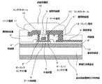
【解決手段】 導電性金属基板1の上面に、基板絶縁層2を介して、TFTを形成する半導体4とゲート電極7とソース電極11とドレイン電極12が形成されている。導電性金属基板1の下面には、該基板1の応力による反りを制御するための基板絶縁層兼応力制御膜3が形成されている。
【選択図】 図1PROBLEM TO BE SOLVED: To adversely affect display device manufacturing due to warpage of a substrate when the substrate is made flexible.
A semiconductor, a gate electrode, a source electrode, and a drain electrode that form a TFT are formed on the upper surface of a conductive metal substrate through a substrate insulating layer. On the lower surface of the conductive metal substrate 1, a substrate insulating layer / stress control film 3 for controlling warpage due to stress of the substrate 1 is formed.
[Selection] Figure 1
Description
本発明は表示装置及びその製造方法に係り、特に導電性のフレキシブル基板または、耐熱性に優れたプラスチック基板に、マトリクス配線を設けた表示装置に関する。 The present invention relates to a display device and a manufacturing method thereof, and more particularly to a display device in which matrix wiring is provided on a conductive flexible substrate or a plastic substrate having excellent heat resistance.
薄膜トランジスタ(以下、TFTと記す)は液晶表示素子やEL表示素子、または電気泳動表示装置などに用いられ、例えば電気泳動表示装置においては、各画素において泳動液室内に封入されたトナーに電界をかける為に制御電極電位を制御する為の能動素子として用いられる。 Thin film transistors (hereinafter referred to as TFTs) are used in liquid crystal display elements, EL display elements, electrophoretic display devices, and the like. For example, in an electrophoretic display device, an electric field is applied to toner enclosed in an electrophoretic liquid chamber in each pixel. Therefore, it is used as an active element for controlling the control electrode potential.
各画素に設けたTFTに用いられる半導体膜には非晶質のシリコン薄膜(a−Si薄膜)や多結晶のシリコン薄膜(poly−Si薄膜)がある。 A semiconductor film used for a TFT provided in each pixel includes an amorphous silicon thin film (a-Si thin film) and a polycrystalline silicon thin film (poly-Si thin film).
従来これらの技術は、例えば表示装置である液晶ディスプレイ用途ではガラスを基板として用いる事が多く、それゆえ、用途にもよるが、耐衝撃性や、柔軟性については十分ではない。 Conventionally, these techniques often use glass as a substrate in a liquid crystal display application, for example, as a display device. Therefore, depending on the application, impact resistance and flexibility are not sufficient.
また、昨今、前述したような電気泳動を用いた表示装置として、従来実現し得なかった薄く、丈夫、かつ、紙の様なしなやかなディスプレイの開発も盛んに行われだしている。 In addition, recently, as a display device using electrophoresis as described above, development of a thin, durable, and paper-like display that could not be realized in the past has been actively conducted.
それに伴い、表示素子を駆動する為のTFTバックプレーンも、従来のガラスではなく、薄い金属板や、プラスチック上に形成する事が考えられている。 Accordingly, it is considered that a TFT backplane for driving the display element is formed on a thin metal plate or plastic instead of the conventional glass.
例えば、特許文献1にステンレス(以下、SUSと記す(Steel Use Stainless))基板上にTFTバックプレーンを形成する為の技術が開示されている。
しかしながら、特許文献1のようにSUS基板上に複数の層にわたり材料を形成すると、例えば金属板厚が薄くなり柔軟性が高くなった場合、導電性基板の絶縁の為に用いられる絶縁層や、その他TFTバックプレーンを形成するゲート絶縁層や、配線層、半導体層などの引っ張り又は圧縮応力のためSUS基板に反りが発生する。SUS基板がその周辺部が持ち上がって凹形に反った場合は、露光や、ドライエッチングを始めとする製造工程時にステージに基板を静電吸着や真空吸着し難くなることや、大きな反りによりマスクアライメントが難しくなる等の問題が生じる。
However, when a material is formed over a plurality of layers on a SUS substrate as in
この事は、SUS基板ばかりでなくプラスチック基板においても同様の事がいえ、該プラスチック基板は必ずしも基板絶縁層を設ける必要は無いが、柔軟性が高くなることで、TFTバックプレーンを形成する各膜の引っ張り又は圧縮応力のため基板に反りが生じ、同様の問題が生じる。 This is true not only for SUS substrates but also for plastic substrates. The plastic substrate does not necessarily have to be provided with a substrate insulating layer, but the flexibility of each film that forms the TFT backplane is increased. Due to the tensile or compressive stress of the substrate, the substrate is warped and the same problem occurs.
そこで本発明の目的は、上記従来技術の問題に鑑み、基板に柔軟性を持たせた場合の該基板の反りが表示装置製造に悪影響を及ぼさないように構成された表示装置用基板及び、これを用いた表示装置を提供することにある。 Accordingly, an object of the present invention is to provide a display device substrate configured so that warpage of the substrate when the substrate is made flexible does not adversely affect display device manufacture, in view of the above-described problems of the prior art. It is to provide a display device using the above.
上記目的を達成するために、本発明は、画素毎に配置された能動素子と、該能動素子の各々に対応して設けられた配線とを、基板の一面に備える表示装置用基板において、前記基板の前記能動素子と前記配線が形成された面とは反対側の面に、前記基板にかかる応力を制御する応力制御膜が設けられていることを特徴とする。 In order to achieve the above object, the present invention provides a display device substrate comprising active elements arranged for each pixel and wiring provided corresponding to each of the active elements on one surface of the substrate. A stress control film for controlling stress applied to the substrate is provided on a surface of the substrate opposite to the surface on which the active element and the wiring are formed.
上記のような応力制御膜を備えることにより、前記能動素子と前記配線が形成された面を上側にした際に凹形に反らないように、この反り加減を制御することが可能になる。基板形状が凸形または平坦な状態になれば、この表示装置用基板をステージに吸着させることが容易となり、表示装置用基板の上面に半導体を作り込む場合の露光やエッチングなどが精度良く実施できる。 By providing the stress control film as described above, it is possible to control this warpage so that it does not warp in a concave shape when the surface on which the active element and the wiring are formed is turned upward. If the substrate shape is convex or flat, the display device substrate can be easily adsorbed to the stage, and exposure and etching can be performed accurately when a semiconductor is formed on the upper surface of the display device substrate. .
また、本発明は、上記のような表示装置用基板を用いた表示装置を提供することができる。その一つとして、前記表示装置用基板と対向配置された基板を有し、該基板と前記表示装置用基板の間に電気泳動粒子と該電気泳動粒子を分散させている媒質とを備えている表示装置を提供することができる。 Further, the present invention can provide a display device using the display device substrate as described above. As one of them, an electrophoretic particle and a medium in which the electrophoretic particles are dispersed are provided between the substrate and the display device substrate. A display device can be provided.
本発明によれば、可撓性があり割れにくいフレキシブルな基板を用いた際にも、各配線やTFTなどの能動素子層の応力に起因して生じる、基板の反りを制御することで、プロセス上重要な、ステージへの基板吸着等が容易になる。これにより、露光や、ドライエッチングを始めとする工程を容易にし、その結果として、良好な性能のTFT等を作製することができる。 According to the present invention, even when a flexible substrate that is flexible and hard to break is used, the warpage of the substrate caused by the stress of each active element layer such as each wiring or TFT is controlled. It is easy to attract the substrate to the stage. As a result, steps such as exposure and dry etching can be facilitated, and as a result, a TFT or the like having good performance can be manufactured.
以下、本発明の実施の形態について図面を参照して説明する。なお、以下の実施形態は一例であり、本発明はこれら実施形態により限定を受けるものではない。 Hereinafter, embodiments of the present invention will be described with reference to the drawings. In addition, the following embodiment is an example and this invention is not limited by these embodiment.
(第1の実施形態)
本発明の第1の実施形態について、図1を用いて説明する。図1は、本発明の第1の実施形態となるTFTの構造を説明するための縦断面図である。
(First embodiment)
A first embodiment of the present invention will be described with reference to FIG. FIG. 1 is a longitudinal sectional view for explaining the structure of a TFT according to the first embodiment of the present invention.
表示素子を駆動するためのTFTは、図1に示すように、厚さが0.2mm、材質がSUS430の導電性金属基板1の上面に基板絶縁層2(材質:SiN)が設けられ、該金属基板1の下面に基板絶縁層兼応力制御膜(材質:SiN)3が設けられている。基板絶縁層2の上面にアモルファスSi(以下、a-Siと記す)の半導体層4が設けられている。半導体層4上にゲート絶縁層6が形成され、このゲート絶縁層6と同じ絶縁層6’,6”が基板絶縁層2上の半導体層4を除いた部分に形成されている。さらに半導体層4上にはゲート絶縁層6を挟むようにオーミックコンタクト層5,5’が設けられている。オーミックコンタクト層5,5’はn型不純物をドーピングしたn+層である。
As shown in FIG. 1, a TFT for driving a display element is provided with a substrate insulating layer 2 (material: SiN) on the upper surface of a
ゲート絶縁層6上にはゲート電極7が設けられている。絶縁層6’上には画素電極8が配線されている。
A
ゲート絶縁層6及びゲート電極7の周囲に層間絶縁層9が形成され、これと同じ層間絶縁層9’が絶縁層6‘’上に、さらに層間絶縁層9”が絶縁層6’上に形成されている。層間絶縁層9,9’上にソース電極11が形成され、コンタクトホール10によりオーミックコンタクト層5’と接触している。また、層間絶縁層9,9”上にドレイン電極12が形成され、コンタクトホール10’によりオーミックコンタクト層5と接触している。
An
そして画素電極8、層間絶縁膜9,9’,9”、ソース電極11およびドレイン電極12が絶縁保護膜13で覆われている。
The
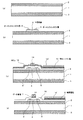
このように構成されたTFTを製造する工程を図2〜図4を用いて順を追って説明する。 A process of manufacturing the TFT configured as described above will be described in order with reference to FIGS.
先ず、図2(a)に示されるように、ブライトアニール研磨を施したSUS430の導電性金属基板1上に、プラズマCVD法を用いて、基板絶縁層2となる窒化シリコン膜を300nm形成した。
First, as shown in FIG. 2A, a 300 nm silicon nitride film serving as a
この時の成膜条件は、アンモニアの流量を300sccm、シランの流量を160ml/min(normal)、プラズマCVDのパワーを800Wとし、基板温度を350℃とした。 The film formation conditions at this time were as follows: the ammonia flow rate was 300 sccm, the silane flow rate was 160 ml / min (normal), the plasma CVD power was 800 W, and the substrate temperature was 350 ° C.
なお、この条件によって成膜された窒化シリコン膜の応力は5.121×10⁻⁵N/cm2であった。 The stress of the silicon nitride film formed under these conditions was 5.121 × 10 −5 N / cm 2 .
次に、導電性金属基板1の裏面と(基板絶縁層2と反対の面)なる面にプラズマCVD法を用いて、基板絶縁層兼応力制御膜3となる窒化シリコン膜を400nm形成した。
Next, a silicon nitride film serving as the substrate insulating layer /
この時の成膜条件は、アンモニアの流量を200ml/min(normal)、シランの流量を160ml/min(normal)、プラズマCVDのパワーを1350Wとし、基板温度を350℃とした。 The film forming conditions at this time were as follows: the ammonia flow rate was 200 ml / min (normal), the silane flow rate was 160 ml / min (normal), the plasma CVD power was 1350 W, and the substrate temperature was 350 ° C.
なお、この条件による成膜された窒化シリコン膜の応力は−5.581×10⁻⁵N/cm2であった。この、応力制御膜の膜質、膜厚等の設計方法としては、シミュレーションによるもの、またはガラス基板等の問題の生じにくい基板上に実際のプロセスでTFTを形成して応力を測定する方法が考えられる。基板を平坦面に置いた場合に凸形状にするのであれば、何れの方法においても条件を決めることは可能である。また、設計自体は各膜を成膜温度と膜厚を振った際のデータを取って応力制御膜の条件(膜厚、温度)を決定していく。 The stress of the silicon nitride film formed under these conditions was −5.581 × 10 −5 N / cm 2 . As a design method of the film quality, film thickness, etc. of the stress control film, a method of measuring stress by forming a TFT by an actual process on a substrate which is difficult to cause a problem such as a simulation or a glass substrate is conceivable. . The condition can be determined by any method as long as the substrate has a convex shape when placed on a flat surface. Also, the design itself determines the conditions (film thickness and temperature) of the stress control film by taking data when the film formation temperature and film thickness are varied for each film.
この時点において、上記のように導電性金属基板1、基板絶縁層2、基板絶縁層兼応力制御膜3からなる基板を平坦な台の上に乗せたところ、基板周辺に対し基板中央部が高く凸形になっている事が確認できた。なお、簡略化の為、図示はしていない。
At this point, when the substrate composed of the
これにより、ステージへの静電吸着を行う際に従来のように、周辺が持ち上がって凹形になっている場合と異なり、確実にチャックが行われ、その結果、基板はステージにならい略平坦な状態となる。 As a result, when performing electrostatic attraction to the stage, unlike the conventional case where the periphery is raised and recessed, the chuck is reliably performed, and as a result, the substrate is substantially flat following the stage. It becomes a state.
次に、半導体層4となるa-Siを200nmの厚さにプラズマCVD法を用いて形成した。この時の成膜条件は、シランの流量を225ml/min(normal)、水素の流量を1000ml/min(normal)、プラズマCVDのパワーを150Wとし、基板温度を350℃とした。
Next, a-Si to be the
また、オーミックコンタクト層5となるn+を70nmの厚さにプラズマCVD法を用いて形成した。この時の成膜条件は、シランの流量を225ml/min(normal)、水素の流量を1000ml/min(normal)、リン化水素の流量を500ml/min(normal)、プラズマCVDのパワーを200Wとし、基板温度を350℃とした。
Further, n + to be the
その後、a-Si層とn+層の上に既知の方法によりフォトレジストの所望の形状のパターンを形成した(不図示)。そのフォトレジストパターンをマスクとしてRIE(Reactive Ion Etching)によりエッチングを行い、さらに、a-Si層上のn+層の一部を上記方法と同様の方法にて取り除き、図2(b)に示すように、フォトレジスト以外の部分のa-Siまたはn+を完全に除去し、半導体層4及びオーミックコンタクト層5,5’を作製した。この時のエッチングの条件はエッチングガスとしてCF4、O2、エッチング圧力3Paの条件で行った。
Thereafter, a pattern of a desired shape of a photoresist was formed on the a-Si layer and the n + layer by a known method (not shown). Etching is performed by RIE (Reactive Ion Etching) using the photoresist pattern as a mask, and a part of the n + layer on the a-Si layer is removed by a method similar to the above method, as shown in FIG. As described above, a-Si or n + in portions other than the photoresist was completely removed, and the
その上に、図2(c)に示すように、ゲート絶縁層6、絶縁層6,6’となる窒化シリコン膜16をプラズマCVD法を用いて、200nm形成した。
On top of this, as shown in FIG. 2C, a
この時の成膜条件は、アンモニアの流量を200ml/min(normal)、シランの流量を160ml/min(normal)、プラズマCVDのパワーを1000Wとし、基板温度を350℃とした。 The film forming conditions at this time were as follows: the ammonia flow rate was 200 ml / min (normal), the silane flow rate was 160 ml / min (normal), the plasma CVD power was 1000 W, and the substrate temperature was 350 ° C.
その上に、ゲート電極7及び画素電極8となるAlCu15をスパッタ法にて膜厚が200nmとなるように形成した。
On top of this,
この時の成膜条件は、ターゲットに2wt%のCuを含有したAlを用い、Ar流量を50ml/min(normal)、スパッタ室の圧力を0.1Pa、DCパワー密度を7W/cm2、基板温度を100℃とした。 The film forming conditions are as follows: Al containing 2 wt% Cu as a target, Ar flow rate of 50 ml / min (normal), sputtering chamber pressure of 0.1 Pa, DC power density of 7 W / cm 2 , substrate The temperature was 100 ° C.
その上に既知の方法にてフォトレジストを塗布した後に所定の形状にパターニングし、ゲート電極7及び画素電極8を形成するときのフォトレジストパターン14、14′を形成した。
A photoresist was applied thereon by a known method and then patterned into a predetermined shape to form
次に、図2(d)に示すように、フォトレジストパターン14、14′をマスクとしてRIE法によりゲート電極7及び画素電極8を形成した。この時、AlCu層のRIEにおいては、エッチングガスとしてCl2、BCl3、エッチング圧力3Paの条件で行った。
Next, as shown in FIG. 2D, the
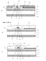
次に、図3(a)に示すように、既知の方法にてフォトレジストを塗布した後に所定の形状にパターニングしたフォトレジストパターン15、15’をマスクとし、RIE法により窒化シリコン層16をエッチングし、ゲート絶縁層6を形成した。このときの窒化シリコンのRIEにおいては、エッチングガスとしてSF6、O2、エッチング圧力3Paの条件で行った。
Next, as shown in FIG. 3A, the
そして、図3(b)に示すように、フォトレジストパターン14、14’、15、15’を取り除いた後、層間絶縁層9、9’、9”となる窒化シリコン層17をゲート絶縁層6の成膜時と同様の条件で600nmの厚さに形成した。
Then, as shown in FIG. 3B, after removing the
次に、図3(c)に示すように、既知の方法にてフォトレジストを塗布した後に所定の形状にパターニングし、RIE法により窒化シリコン層17をパターニングすると共にコンタクトホール10、10′を形成して層間絶縁層9、9’、9”を作製した。ガス種としてはSF6とO2の混合ガスを用い、圧力3Pa、RFパワー1.5kWでレジスト後退法により、コンタクトホール10、10’をテーパー角50°で形成した(図3(c)では簡略化のためにテーパーが描かれていない。)。
Next, as shown in FIG. 3C, a photoresist is applied by a known method and then patterned into a predetermined shape, and the silicon nitride layer 17 is patterned by RIE and contact holes 10, 10 'are formed. Thus,
図4(a)に示すように、その上に電極となるAlCu膜をスパッタ法により前述のゲート電極7の作製時と同様の成膜条件で膜厚が700nmとなるように形成した。その後、既知の方法で所望の形状にパターニングし、ソース電極11とドレイン電極12を形成した。
As shown in FIG. 4A, an AlCu film serving as an electrode was formed thereon by sputtering so as to have a film thickness of 700 nm under the same film formation conditions as those for manufacturing the
更に、図4(b)に示すように、この上に絶縁保護層13として窒化シリコンを、先の層間絶縁膜9の成膜時と同様の条件で、CVD法にて500nmの厚さに形成した。
Further, as shown in FIG. 4B, silicon nitride is formed thereon as an insulating protective layer 13 to a thickness of 500 nm by the CVD method under the same conditions as those for forming the
このように、熱伝導率の低いa−Siを厚く成膜することにより、断熱層として機能させることが出来る。この方法で作製したTFTはON/OFF比=1×106、Vth=1.2V、μ=0.4cm2/V・secという良好な性能であった。 In this manner, by thickly forming a-Si having a low thermal conductivity, it can function as a heat insulating layer. The TFT fabricated by this method had good performance with an ON / OFF ratio = 1 × 10 6 , Vth = 1.2 V, and μ = 0.4 cm 2 / V · sec.
更に、この基板をリア基板とし、これと対向するようフェース基板を配置し、両基板間に電気泳動粒子とこれを分散させる媒質を備えた電気泳動表示装置(EPID)を作製したところ、良好な表示装置を作ることが出来た。 Further, when this substrate is used as a rear substrate, a face substrate is disposed so as to face the rear substrate, and an electrophoretic display device (EPID) including electrophoretic particles and a medium for dispersing the electrophoretic particles is produced between both substrates. We were able to make a display device.
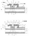
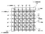
図5は、本実施形態における300行×250列のTFTアクティブマトリクスアレイの一部分の模式図である。 FIG. 5 is a schematic view of a part of a 300 × 250 column TFT active matrix array in the present embodiment.
同図において、表示パネル100は、ゲート電極106とソース電極111とがマトリクス状に配置されたゲート電極106及びソース電極111と、ゲート電極106を駆動するゲート線駆動回路125とソース電極111を駆動するソース線駆動回路126とを有している。例えば、ゲート線駆動電圧はオン電圧+20V、オフ電圧−20Vであり、ソース線駆動電圧は0V〜15Vである。なお、符号109はアモルファス半導体層であるTFTを、符号114は画素電極を示している。
In the figure, the
本実施形態では基板として光が透過しないSUSを用いているため、反射式の表示装置として構成した。その結果良好な表示状態を得ることが出来た。 In this embodiment, since SUS which does not transmit light is used as the substrate, it is configured as a reflective display device. As a result, a good display state could be obtained.
なお、本実施形態においては、表示装置用基板の応力コントロールを窒化シリコン膜の、成膜条件とその膜厚を制御する事で行ったが、窒化シリコン膜に限った事ではなく、例えばアモルファスシリコン膜を、応力制御膜として用いても何ら問題はなく、膜の応力制御が可能な膜であれば同様の効果を得ることが可能である。また、応力制御膜の膜厚が一定の条件においても、該応力制御膜の成膜条件を管理する事で基板に対する応力を制御したり、あるいは、応力制御膜の成膜条件を管理し、該応力制御膜の膜質が一定であっても、基板に対する応力を制御する為に、応力制御膜の膜厚を管理する方法をとってもよい。 In this embodiment, the stress of the display device substrate is controlled by controlling the film formation conditions and the film thickness of the silicon nitride film. However, the present invention is not limited to the silicon nitride film. For example, amorphous silicon is used. There is no problem even if the film is used as a stress control film, and the same effect can be obtained as long as the film can control the stress of the film. Further, even when the film thickness of the stress control film is constant, the stress on the substrate is controlled by managing the film formation conditions of the stress control film, or the film formation conditions of the stress control film are managed. Even if the film quality of the stress control film is constant, a method of managing the film thickness of the stress control film may be used in order to control the stress on the substrate.
さらに、本実施形態では、基板としてSUSを用いているが、可撓性があり割れにくい基板であれば如何なる材質の基板にも本発明の思想を適用することができ、例えば、金属のみならず樹脂を用いたフレキシブル基板にも適用可能である。 Furthermore, in this embodiment, SUS is used as the substrate, but the idea of the present invention can be applied to any material substrate as long as it is flexible and difficult to break. The present invention can also be applied to a flexible substrate using a resin.
また、本実施形態では、トップゲート型構造のTFTを用い表示装置を製造したが、この構成に限られず、いわゆる単純マトリクス構成や、TFD構成においても適用することが可能であり、また、TFT構造においても、ボトムゲート型構造においても応力制御膜を用いることで製造する事が可能である。 In this embodiment, a display device is manufactured using a TFT having a top gate structure. However, the present invention is not limited to this configuration, and can be applied to a so-called simple matrix configuration or TFD configuration. However, even a bottom gate type structure can be manufactured by using a stress control film.
さらに、本実施形態では、アモルファスシリコンTFTを用いたが、エキシマレーザアニールを施すなどして、多結晶化されたいわゆるポリシリコンTFTに、応力制御膜の条件を変えて用いる事で、液晶表示装置や、EL表示装置として適用しても何ら問題はない。 Furthermore, in this embodiment, an amorphous silicon TFT is used. However, a liquid crystal display device can be used by changing the conditions of the stress control film to a polycrystallized so-called polysilicon TFT by excimer laser annealing or the like. There is no problem even if it is applied as an EL display device.
1 導電性金属基板
2 基板絶縁層
3 基板絶縁層兼応力制御膜
4 半導体層
5、5′ オーミックコンタクト層
6 ゲート絶縁層
6’、6” 絶縁層
7 ゲート電極
8 画素電極
9、9’、9” 層間絶縁層
10、10’ コンタクトホール
11 ソース電極
12 ドレイン電極
13 絶縁保護膜
14、14’、15、15’ フォトレジストパターン
15 AlCu
16、17 窒化シリコン層
100 表示パネル
106 ゲート電極
109 TFT
111 ソース電極
114 画素電極
125 ゲート線駆動回路
126 ソース線駆動回路
DESCRIPTION OF
16, 17
111
Claims (7)
前記基板の前記能動素子と前記配線が形成された面とは反対側の面に、前記基板にかかる応力を制御する応力制御膜が設けられていることを特徴とする表示装置用基板。 In a display device substrate comprising active elements arranged for each pixel and wiring provided corresponding to each of the active elements on one surface of the substrate,
A substrate for a display device, wherein a stress control film for controlling a stress applied to the substrate is provided on a surface of the substrate opposite to a surface on which the active element and the wiring are formed.
前記表示装置用基板と対向配置された基板を有し、該基板と前記表示装置用基板の間に電気泳動粒子と該電気泳動粒子を分散させている媒質とを備えている表示装置。 A display device using the display device substrate according to claim 1,
A display device comprising a substrate disposed opposite to the display device substrate, and comprising an electrophoretic particle and a medium in which the electrophoretic particle is dispersed between the substrate and the display device substrate.
Priority Applications (1)
| Application Number | Priority Date | Filing Date | Title |
|---|---|---|---|
| JP2004109097A JP2005292574A (en) | 2004-04-01 | 2004-04-01 | Display device substrate and display device using the same |
Applications Claiming Priority (1)
| Application Number | Priority Date | Filing Date | Title |
|---|---|---|---|
| JP2004109097A JP2005292574A (en) | 2004-04-01 | 2004-04-01 | Display device substrate and display device using the same |
Publications (1)
| Publication Number | Publication Date |
|---|---|
| JP2005292574A true JP2005292574A (en) | 2005-10-20 |
Family
ID=35325542
Family Applications (1)
| Application Number | Title | Priority Date | Filing Date |
|---|---|---|---|
| JP2004109097A Pending JP2005292574A (en) | 2004-04-01 | 2004-04-01 | Display device substrate and display device using the same |
Country Status (1)
| Country | Link |
|---|---|
| JP (1) | JP2005292574A (en) |
Cited By (5)
| Publication number | Priority date | Publication date | Assignee | Title |
|---|---|---|---|---|
| EP1659621A1 (en) * | 2004-11-20 | 2006-05-24 | Samsung SDI Co., Ltd. | Substrate including a deformation preventing layer |
| JP2015062079A (en) * | 2008-07-10 | 2015-04-02 | 株式会社半導体エネルギー研究所 | Electronic paper |
| CN107611012A (en) * | 2017-08-31 | 2018-01-19 | 长江存储科技有限责任公司 | A kind of stress control method and structure of prefabricated back film |
| CN108231730A (en) * | 2018-01-02 | 2018-06-29 | 京东方科技集团股份有限公司 | A kind of preparation method of display panel, electronic equipment and display panel |
| CN108490698A (en) * | 2018-06-11 | 2018-09-04 | 深圳市德安里科技有限公司 | A kind of liquid crystal handwriting board device |
-
2004
- 2004-04-01 JP JP2004109097A patent/JP2005292574A/en active Pending
Cited By (6)
| Publication number | Priority date | Publication date | Assignee | Title |
|---|---|---|---|---|
| EP1659621A1 (en) * | 2004-11-20 | 2006-05-24 | Samsung SDI Co., Ltd. | Substrate including a deformation preventing layer |
| US7816666B2 (en) | 2004-11-20 | 2010-10-19 | Samsung Mobile Display Co., Ltd. | Preventing substrate deformation |
| JP2015062079A (en) * | 2008-07-10 | 2015-04-02 | 株式会社半導体エネルギー研究所 | Electronic paper |
| CN107611012A (en) * | 2017-08-31 | 2018-01-19 | 长江存储科技有限责任公司 | A kind of stress control method and structure of prefabricated back film |
| CN108231730A (en) * | 2018-01-02 | 2018-06-29 | 京东方科技集团股份有限公司 | A kind of preparation method of display panel, electronic equipment and display panel |
| CN108490698A (en) * | 2018-06-11 | 2018-09-04 | 深圳市德安里科技有限公司 | A kind of liquid crystal handwriting board device |
Similar Documents
| Publication | Publication Date | Title |
|---|---|---|
| KR100793628B1 (en) | Semiconductor device and method of manufacturing same | |
| JP4718999B2 (en) | Thin film transistor substrate manufacturing method and liquid crystal display device thin film transistor manufacturing method | |
| US8158982B2 (en) | Polysilicon thin film transistor device with gate electrode thinner than gate line | |
| US7595849B2 (en) | Display device and manufacturing method thereof | |
| JP2010135384A (en) | Thin film transistor array substrate, manufacturing method thereof, and liquid crystal display device | |
| KR100731738B1 (en) | Thin film transistor, flat panel display and manufacturing method | |
| US7507612B2 (en) | Flat panel display and fabrication method thereof | |
| CN101414564B (en) | Method for manufacturing low-temperature polycrystalline silicon film transistor | |
| JP2005292574A (en) | Display device substrate and display device using the same | |
| JP2008042218A (en) | Method for manufacturing thin film transistor panel | |
| US7177003B2 (en) | LCD with gate and data lines formed of copper and an aluminum under-layer | |
| JP2007027710A (en) | Contact hole forming method and thin film transistor substrate manufacturing method using the same | |
| JP2009289890A (en) | Semiconductor device and method of manufacturing the same | |
| JP2006505121A (en) | THIN FILM TRANSISTOR AND METHOD FOR PRODUCING THIN FILM TRANSISTOR | |
| JP2007180511A (en) | Thin film transistor substrate, manufacturing method thereof, and display panel having the same | |
| KR100425159B1 (en) | Method For Fabricating The Polysilicon Thin Film Transistor And Method For Fabricating Liquid Crystal Display Device By Using Said Metod | |
| JPH11265000A (en) | Liquid crystal display device and manufacturing method thereof | |
| KR101022569B1 (en) | Thin film transistor and its manufacturing method | |
| JP4052804B2 (en) | Electrode substrate and method for producing electrode substrate | |
| JPH0677486A (en) | Thin-film transistor element | |
| JP4780924B2 (en) | Manufacturing method of matrix array substrate | |
| JP2008021722A (en) | TFT manufacturing method and manufacturing apparatus thereof | |
| KR102135911B1 (en) | Manufacturing method of thin film transistor array substrate | |
| JP4155039B2 (en) | Thin film transistor, electro-optical device, electronic equipment | |
| JP2010147303A (en) | Thin-film transistor, method of manufacturing the same, thin-film transistor array substrate, and display device |