JP2005292223A - Electro-optical device and electronic equipment - Google Patents
Electro-optical device and electronic equipment Download PDFInfo
- Publication number
- JP2005292223A JP2005292223A JP2004103420A JP2004103420A JP2005292223A JP 2005292223 A JP2005292223 A JP 2005292223A JP 2004103420 A JP2004103420 A JP 2004103420A JP 2004103420 A JP2004103420 A JP 2004103420A JP 2005292223 A JP2005292223 A JP 2005292223A
- Authority
- JP
- Japan
- Prior art keywords
- electro
- substrate
- optical device
- pixel electrode
- wiring
- Prior art date
- Legal status (The legal status is an assumption and is not a legal conclusion. Google has not performed a legal analysis and makes no representation as to the accuracy of the status listed.)
- Withdrawn
Links
Images


Landscapes
- Liquid Crystal (AREA)
- Devices For Indicating Variable Information By Combining Individual Elements (AREA)
Abstract
Description
本発明は、電気光学装置及び電子機器に関する。 The present invention relates to an electro-optical device and an electronic apparatus.
従来、液晶装置等の電気光学装置に用いるスイッチング素子として二端子型の非線形素子が知られており、例えば特許文献1又は特許文献2に開示されたような構成のものがある。
上記特許文献1及び特許文献2では、二端子型の非線形素子としてMIM素子を備えた液晶表示装置が開示されており、該MIM素子と画素電極とが絶縁層を介して接続されている。しかしながら、これら各特許文献の構成によると、MIM素子上に形成されたコンタクトホールを介して該MIM素子と画素電極とを電気的に接続しているため、該コンタクトホールの開口径が小さくなり、コンタクト抵抗が高くなる問題を有している。この場合、画素電極への通電特性が低下し、当該液晶表示装置の表示特性の低下を引き起こす場合もある。 Patent Document 1 and Patent Document 2 disclose a liquid crystal display device including a MIM element as a two-terminal nonlinear element, and the MIM element and the pixel electrode are connected via an insulating layer. However, according to the configuration of each of these patent documents, since the MIM element and the pixel electrode are electrically connected via the contact hole formed on the MIM element, the opening diameter of the contact hole is reduced, There is a problem that the contact resistance becomes high. In this case, the current-carrying characteristic to the pixel electrode is lowered, and the display characteristic of the liquid crystal display device may be lowered.
本発明は上述の問題を解決するためになされたもので、非線形素子を備える電気光学装置であって、該素子と画素電極との電気的接続を良好に保つことが可能な構成を具備した電気光学装置を提供することを目的としている。さらに、本発明は、このような電気光学装置を備えた信頼性の高い電子機器を提供することを目的としている。 The present invention has been made to solve the above-described problems, and is an electro-optical device including a non-linear element, and an electric device having a configuration capable of maintaining good electrical connection between the element and the pixel electrode. An object is to provide an optical device. Another object of the present invention is to provide a highly reliable electronic apparatus including such an electro-optical device.
上記の目的を達成するために、本発明の電気光学装置は、基板と、前記基板上に形成されたデータ線と、前記基板上に形成されるとともに前記データ線と電気的に接続されてなり、第1導電層と第2導電層との間に絶縁層を備える構成の非線形素子であるスイッチング素子と、前記スイッチング素子から延設してなる配線と、前記データ線、前記スイッチング素子及び前記配線を覆う形にて前記基板上に形成された層間絶縁層と、該層間絶縁層上に形成され、前記層間絶縁層に形成されたコンタクトホールを介して、前記配線と電気的に接続されてなる画素電極とを具備することを特徴とする。 In order to achieve the above object, an electro-optical device of the present invention includes a substrate, a data line formed on the substrate, and formed on the substrate and electrically connected to the data line. A switching element which is a nonlinear element having an insulating layer between the first conductive layer and the second conductive layer, a wiring extending from the switching element, the data line, the switching element and the wiring An interlayer insulating layer formed on the substrate so as to cover the substrate, and formed on the interlayer insulating layer and electrically connected to the wiring via a contact hole formed in the interlayer insulating layer. And a pixel electrode.
スイッチング素子として非線形素子を用いた場合、該非線形素子は第1導電層と第2導電層との間の容量によって駆動電圧が定まるが、各導電層の対向する面積が大きくなると、容量が大きくなって大きな駆動電圧を必要とする。したがって、高速、高精細な駆動を行うために、各導電層の対向する面積は小さい方が好ましい。一方、スイッチング素子と画素電極と接続するためのコンタクトホールは、その開口面積が大きいほど、コンタクト抵抗が小さくなって高速、高精細な駆動が可能となる。つまり、高速、高精細な駆動を行うためには、スイッチング素子たる非線形素子は小さくしたい一方で、コンタクトホールは大きくしたい要求がある。 When a non-linear element is used as the switching element, the driving voltage of the non-linear element is determined by the capacitance between the first conductive layer and the second conductive layer. However, as the opposing area of each conductive layer increases, the capacitance increases. Large driving voltage is required. Therefore, in order to perform high-speed and high-definition driving, it is preferable that the opposing areas of the conductive layers are small. On the other hand, as the contact hole for connecting the switching element and the pixel electrode has a larger opening area, the contact resistance becomes smaller and high-speed, high-definition driving is possible. In other words, in order to perform high-speed, high-definition driving, there is a demand for reducing the nonlinear element as a switching element while increasing the contact hole.
ところが、従来の技術のように非線形素子上にコンタクトホールを形成した場合には、スイッチング素子とコンタクトホールの接続面において、接続部の素子の大きさと接続部のコンタクトホールの大きさを同じにしなければならない。つまり、従来の技術では、スイッチング素子の接続部面積を小さくすればコンタクトホールの開口面積は小さくなり、コンタクトホールの開口面積を大きくすればスイッチング素子の接続部面積が大きくなってしまうものである。 However, when a contact hole is formed on a nonlinear element as in the prior art, the size of the element at the connection portion and the size of the contact hole at the connection portion must be the same on the connection surface between the switching element and the contact hole. I must. That is, in the conventional technique, if the connection area of the switching element is reduced, the opening area of the contact hole is reduced, and if the opening area of the contact hole is increased, the connection area of the switching element is increased.
そこで、上述した本発明の電気光学装置によると、スイッチング素子たる非線形素子と画素電極とを接続するためのコンタクトホールを、スイッチング素子から延設された配線上に形成しており、つまり層間絶縁層のうちスイッチング素子の直上以外の領域(スイッチング素子から配線により延設された領域)に形成しているため、スイッチング素子の導電層の面積を小さくする一方、コンタクトホールの開口面積を十分に大きくすることができるようになる。したがって、当該電気光学装置において高速で高精細な駆動が可能となり、例えばこれを表示装置として用いた場合には、高速動画に適した表示特性に優れるものとなる。なお、詳しくは、前記コンタクトホールは、前記スイッチング素子のうち前記層間絶縁層側に形成された第2導電層上以外の領域に形成することができる。 Therefore, according to the electro-optical device of the present invention described above, the contact hole for connecting the nonlinear element serving as the switching element and the pixel electrode is formed on the wiring extending from the switching element, that is, the interlayer insulating layer. The area of the conductive layer of the switching element is reduced while the opening area of the contact hole is sufficiently increased. Will be able to. Therefore, the electro-optical device can be driven at high speed and with high definition. For example, when the electro-optical device is used as a display device, the display characteristics suitable for high-speed moving images are excellent. In detail, the contact hole can be formed in a region other than the second conductive layer formed on the interlayer insulating layer side of the switching element.
本発明の電気光学装置において、前記スイッチング素子と前記画素電極とが平面的に重なって形成されているものとすることができる。この場合、当該電気光学装置を表示装置として用いた場合、該スイッチング素子の形成領域は非表示部(非有効画素領域)となる一方、スイッチング素子の非形成領域が表示部(有効画素領域)となる。したがって、表示領域として大きな面積を確保することが可能となる。また、前記コンタクトホールが、前記画素電極と平面的に重なって形成されているものとすることができ、この場合も表示領域として一層面積を確保することができるようになる。 In the electro-optical device according to the aspect of the invention, the switching element and the pixel electrode may be formed so as to overlap in a plane. In this case, when the electro-optical device is used as a display device, the switching element formation region is a non-display portion (non-effective pixel region), while the switching element non-formation region is a display portion (effective pixel region). Become. Therefore, a large area can be secured as a display region. Further, the contact hole may be formed so as to overlap with the pixel electrode in a plan view, and in this case, a further area can be secured as a display region.
また、前記配線は、前記コンタクトホールの直下で該コンタクトホールの開口面積よりも大きな面積を有してなるものとすることができる。このような配線を形成することで、スイッチング素子からコンタクトホールまでの電気的接続を確実にとることができるようになり、さらに該配線を遮光性の部材にて形成することで、コンタクトホールの形成領域を該配線にて確実に遮光することができるようになる。 The wiring may have an area directly below the contact hole and larger than the opening area of the contact hole. By forming such a wiring, it is possible to reliably establish an electrical connection from the switching element to the contact hole, and by forming the wiring with a light-shielding member, formation of the contact hole The area can be reliably shielded from light by the wiring.
また、本発明の電気光学装置において、前記基板と対向する対向基板を更に備え、前記基板と前記対向基板との間に、負の誘電異方性を有する液晶が形成されてなるものとすることができる。さらに、前記基板と対向する対向基板を備え、該対向基板には、前記コンタクトホールと平面的に重なる位置に遮光部が形成されているものとすることができる。この場合もコンタクトホールの形成領域を確実に遮光することができるようになる。 The electro-optical device according to the aspect of the invention further includes a counter substrate facing the substrate, and a liquid crystal having negative dielectric anisotropy is formed between the substrate and the counter substrate. Can do. Furthermore, a counter substrate facing the substrate may be provided, and a light shielding portion may be formed on the counter substrate so as to overlap the contact hole in a plan view. Also in this case, the contact hole formation region can be reliably shielded from light.
また、前記配線は、前記スイッチング素子が設けられた領域の延長した領域に設けられてなるものとすることができる。この場合、スイッチング素子と配線との占有面積を極力小さくすることが可能となる。具体的には、前記配線を一直線状に形成し、その配線上に前記コンタクトホールを形成するものとすればよい。 The wiring may be provided in a region extended from the region in which the switching element is provided. In this case, the area occupied by the switching element and the wiring can be minimized. Specifically, the wiring is formed in a straight line, and the contact hole is formed on the wiring.
また、前記配線は、前記コンタクトホールの近傍において、前記コンタクトホールの外形に沿った形状で形成されてなるものとすることができる。詳しくは、前記コンタクトホールの近傍において、前記コンタクトホールの軸断面外形に沿った平面形状で形成されてなるものとすることができる。この場合、配線の占有面積を極力小さくし、且つ上述したコンタクトホールの遮光効果も十分に発現することができる。 Further, the wiring may be formed in a shape along the outer shape of the contact hole in the vicinity of the contact hole. Specifically, it can be formed in the vicinity of the contact hole in a planar shape along the axial cross-sectional outline of the contact hole. In this case, the area occupied by the wiring can be reduced as much as possible, and the above-described light shielding effect of the contact hole can be sufficiently exhibited.
前記層間絶縁膜は、平坦化膜であるものとすることができる。具体的には、前記層間絶縁膜が平坦な表面を有するものとして構成することができる。この場合、例えば当該電気光学装置を液晶装置として用いたときには、液晶の配向乱れを効果的に防止ないし抑制することができ、特に配線及び素子の形成されていない領域を平坦化できるので、液晶配向の乱れを抑制するには好都合である。 The interlayer insulating film may be a planarizing film. Specifically, the interlayer insulating film can be configured to have a flat surface. In this case, for example, when the electro-optical device is used as a liquid crystal device, alignment disorder of the liquid crystal can be effectively prevented or suppressed, and in particular, a region where no wiring and elements are formed can be flattened. It is convenient to suppress the disturbance.
前記配線と前記画素電極が電気的に接続されていない隣接するデータ線との距離は、前記画素電極と前記隣接するデータ線との距離よりも離れているものとすることができる。詳しくは、1つの画素電極(第1画素電極とする)と、これに信号を供給するための配線と、第1画素電極に隣接する第2画素電極に対して信号を供給するためのデータ線(第2データ線とする)との位置関係について、配線と第2データ線との距離が、第1画素電極と第2データ線との距離よりも大きく形成されてなるものとすることができる。この場合、配線と第2データ線との寄生容量を介して、該第2データ線を導通する信号が当該配線に乗ることを防止ないし抑制することができるようになる。 A distance between the wiring and an adjacent data line to which the pixel electrode is not electrically connected may be longer than a distance between the pixel electrode and the adjacent data line. Specifically, one pixel electrode (referred to as a first pixel electrode), a wiring for supplying a signal thereto, and a data line for supplying a signal to a second pixel electrode adjacent to the first pixel electrode With respect to the positional relationship with the second data line, the distance between the wiring and the second data line may be formed larger than the distance between the first pixel electrode and the second data line. . In this case, a signal that conducts the second data line can be prevented or suppressed from entering the wiring through the parasitic capacitance between the wiring and the second data line.
次に、本発明の電子機器は、先に記載の電気光学装置を具備することを特徴とする。ここで、電子機器としては、例えば、携帯電話機、移動体情報端末、時計、ワープロ、パソコンなどの情報処理装置などを例示することができる。このような電子機器によれば、先に記載の電気光学装置を用いているので、高速で高精細の駆動が可能となるとともに、該電気光学装置を表示部として備えている場合には、有効画素面積が大きい視認性に優れた表示を提供することができるようになる。 Next, an electronic apparatus according to an aspect of the invention includes the electro-optical device described above. Here, as an electronic device, information processing apparatuses, such as a mobile telephone, a mobile information terminal, a clock, a word processor, a personal computer, etc. can be illustrated, for example. According to such an electronic apparatus, since the above-described electro-optical device is used, high-speed and high-definition driving is possible, and when the electro-optical device is provided as a display unit, it is effective. A display with a large pixel area and excellent visibility can be provided.
次に、本発明に係る実施の形態について図面を参照しつつ説明する。なお、各図において、各層や各部材を図面上で認識可能な程度の大きさとするため、各層や各部材毎に縮尺を異ならせてある。 Next, embodiments according to the present invention will be described with reference to the drawings. In addition, in each figure, in order to make each layer and each member into a size that can be recognized on the drawing, the scale is varied for each layer and each member.
[電気光学装置]
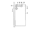
図1は、本発明の電気光学装置の一実施形態である液晶表示装置について、各構成要素とともに示す対向基板側から見た平面図であり、図2は、その要部の断面図である。図3は液晶表示装置の画像表示領域においてマトリクス状に形成された複数の画素における各種素子、配線等の等価回路図である。ここで、本実施形態の電気光学装置は、図示しないバックライトからの光を用いる透過型液晶表示装置であって、スイッチング素子として二端子型非線形素子、ここではTFD(Thin Film Diode)素子を用いたアクティブマトリクス方式の液晶表示装置である。
[Electro-optical device]
FIG. 1 is a plan view of a liquid crystal display device, which is an embodiment of the electro-optical device of the present invention, viewed from the counter substrate side shown together with each component, and FIG. FIG. 3 is an equivalent circuit diagram of various elements and wirings in a plurality of pixels formed in a matrix in the image display region of the liquid crystal display device. Here, the electro-optical device of the present embodiment is a transmissive liquid crystal display device using light from a backlight (not shown), and uses a two-terminal nonlinear element, here a TFD (Thin Film Diode) element, as a switching element. This is an active matrix type liquid crystal display device.
図1及び図2に示すように、本実施の形態の液晶表示装置100は、対をなす下基板110と上基板120とが紫外線硬化性のシール材52によって貼り合わされ、このシール材52によって区画された領域内に液晶50が封入、保持されている。シール材52は、基板面内において閉ざされた環状(枠状)に形成されており、液晶注入口を備えていない構成となっている。つまり、液晶注入口を封止する封止材を備えておらず、環状全体が同一の材料にて連続的に構成されている。なお、液晶注入口を備え、これを封止材により封止した構成のシール材を用いることもできる。
As shown in FIGS. 1 and 2, in the liquid
矩形環状のシール材52のうち、図1に示す下基板110の右辺、左辺(対向した2つの辺)に沿う部分には、下基板110と上基板120との間で電気的に導通するための導電性粒子(基板間導通部)206が含有されている。なお、この導電性粒子206は異方性導電粒子にて構成されている。
In the rectangular ring-shaped
下基板110の内面側には複数の画素電極9がマトリクス状に形成される一方、上基板120の内面側には短冊状のストライプ電極23が形成されており、各電極9,23の内面側には更に配向膜(図示略)が形成されている。なお、画素電極9にはスイッチング素子としてTFD素子4(薄膜ダイオード素子、図4参照)が接続されている。
A plurality of
また、本実施の形態では、上基板120よりも下基板110の外形寸法の方が大きく、上基板120と下基板110の3辺(図1における上辺、右辺、左辺)ではほぼ縁(基板の端面)が揃っているが、上基板120の残りの1辺(図1における下辺)からは下基板110の周縁部が張り出すように配置され、張出領域90を形成している。
張出領域90には、下基板110側に形成された画素電極9を駆動するための第1駆動IC201と、上基板120側に形成されたストライプ電極23を駆動するための第2駆動IC202とが実装されている。なお、各駆動IC201,202には図示しない外部接続端子が形成され、当該液晶表示装置100とは異なる外部機器から表示制御信号等を受信可能な構成となっている。
Further, in the present embodiment, the outer dimension of the
The
第1駆動IC201及び第2駆動IC202は、ともに下基板110上に配設され、しかも矩形状の下基板110の同一の張出領域90に形成されている。第1駆動IC201は、下基板110側に形成された信号線を介してTFD素子4(図4参照)、ひいては画素電極9に信号を送信するためのICであって、該下基板110に形成された配線205を介して信号供給が行われている。
The
第2駆動IC202は下基板110に形成される一方、上基板120に形成されたストライプ電極23に信号を送信するためのICであるため、下基板110に形成された引き廻し配線207を介し、さらにシール材52に形成された導通性粒子206を介してストライプ電極23に信号が供給されるものとなっている。ここで、引き廻し配線207は、図1に示したシール材52の下辺部を跨いで、該シール材52の環状内側から導通性粒子206に接続されている。
Since the
上下基板間の電気的導通は、以下のように行われている。
まず、上基板120に形成されたストライプ電極23は、その一端若しくは両端がシール材52の内部に食い込む形にて延在しており、シール材52内部で導電性粒子206に電気的に接続されている。
一方、下基板110側には、上述した第2駆動IC202(図1参照)と接続する引き廻し配線207が形成されており、引き廻し配線207は、図1に示すように、下基板110の下辺側の張出領域90に実装された第2駆動IC202から、下基板110の左右辺方向に延びるように屈曲して形成されており、下基板110の下辺部においてシール材52を跨いで、該シール材52の内側領域を下基板110の左右辺に沿って縦方向に延びている。そして、所定のストライプ電極23と接続する位置にてシール材52の内部に導通し、導電性粒子206に電気的に接続されている。
Electrical conduction between the upper and lower substrates is performed as follows.
First, the
On the other hand, on the
ここで、導電性粒子206は、異方性導電粒子を用いて構成されており、上下方向の接続が確実なものとなるように、上下に弾性変形した形にて配設されている。該粒子206は、基板貼り合わせ前において、液晶層厚を規定するスペーサー(図示略)の直径よりも0.1μm〜1.0μm程度大きな直径を有したものを用いるのが良く、これを上下に1%〜10%程度圧縮させて用いるのが良い。
Here, the
なお、液晶表示装置100においては、使用する液晶50の種類、すなわちTN(Twisted Nematic)モード、STN(Super Twisted Nematic)モード、VAN(Vertical Aligned Nematic)モード等の動作モードや、ノーマリホワイトモード/ノーマリブラックモードの別に応じて、位相差板、偏光板等が所定の向きに配置されるが、ここでは図示を省略する。
In the liquid
このような構成を有する液晶表示装置100の画像表示領域においては、図3に示すように、複数の画素15がマトリクス状に構成されている。また、図3に示すように、液晶表示装置100は第1駆動IC201及び第2駆動IC202を含んでおり、複数の走査線14(対向電極23に相当)と、該走査線14と交差する複数のデータ線13とが設けられ、データ線13は第1駆動IC201からの信号を、走査線14は第2駆動IC202からの信号を各画素15に供給する。そして、各画素15において、データ線13と走査線14との間にTFD素子4と液晶表示要素16(液晶層)とが直列に接続されている。なお、図3では、TFD素子4がデータ線13側に接続され、液晶表示要素16が走査線14側に接続されているが、これとは逆にTFD素子4を走査線14側に、液晶表示要素16をデータ線13側に設ける構成としても良い。
In the image display region of the liquid
以上のような回路構成により、TFD素子4のスイッチング特性に基づいて液晶表示要素16が駆動制御されるとともに、その液晶表示要素16の駆動に基づいて画素15毎に明暗表示がなされ、液晶表示装置100の表示領域において画像表示が行われるものとされている。以下、TFD素子4及び画素15の構成、並びにTFD素子4を備えた素子基板110の構成について詳細に説明する。
With the circuit configuration as described above, the liquid
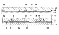
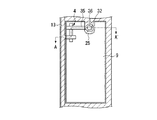
図4は、1画素当りの平面構成を示す図であって、主として画素電極9とTFD素子4及びデータ線13の平面的位置関係を示す図である。また、図5は、下基板(以下、素子基板とも言う)110における1画素当り(隣接する画素の一部を含む)の断面構成を示す図(図4のA−A’断面に相当)であって、主として画素電極9とTFD素子4及びデータ線13の断面的位置関係を示す図である。
FIG. 4 is a diagram showing a planar configuration per pixel, and is a diagram mainly showing a planar positional relationship between the
図4に示すように、本実施形態のTFD素子4は、いわゆるBack to Back構造を有してなり、データ線13と画素電極9とがTFD素子4を介して接続されている。なお、データ線13は、図1及び図2に示すようにシール材52の外側領域(非表示領域)において実装端子(外部接続端子)18に接続され、各種データの入出力が可能な構成となっている。これらTFD素子4、データ線13は、図5に示すように素子基板110上に形成されている。
As shown in FIG. 4, the
素子基板110は、絶縁性及び透明性を有するガラス基板或いはプラスチック基板等からなり、該素子基板110上には、下地絶縁膜3を介してデータ線13及びTFD素子4が形成されている。データ線13は、クロムによって形成されてなり、画素電極9の非形成領域に配設されており、画素電極9の形成領域に配設されたTFD素子4と電気的に接続されている。つまり、データ線13は画素電極9と平面的に重ならない位置に配設され、TFD素子4は画素電極9と平面的に重なる位置に配設されている。
The
データ線13と接続されてなるTFD素子4は、タンタル及びクロムによって絶縁膜を狭持した構成を有している。詳しくは、TFD素子4は、素子基板110上に下地絶縁膜3を介して形成されており、タンタルにて構成された第1導電膜6と、第1導電膜6の表面を酸化してなる酸化タンタル(Ta2O5)にて構成された絶縁膜(絶縁層)7と、該絶縁膜7上に配設されクロムにて構成された第2導電膜8とを素子基板110側から備えてなるものである。そして、第2導電膜8の一部がデータ線13と接続され、異なる一部が画素電極9と電気的に繋がる金属配線35と接続されている。
The
データ線13、TFD素子4及び金属配線35を含む素子基板110には、これらを覆う形にて層間絶縁膜34が形成されている。層間絶縁膜34はシリコン酸化膜或いはアクリル樹脂等の透光性絶縁膜にて構成されている。そして、この層間絶縁膜34上にITO等の透明導電材料からなる画素電極9が形成されている。なお、層間絶縁膜34には、画素電極9とTFD素子4とを電気的に接続するためのコンタクトホール32が、TFD素子4とは重ならない位置(つまりTFD素子4の直上以外の領域)であって、画素電極9と平面的に重なる位置に配設されている。
On the
上述の通り、画素電極9はコンタクトホール32を介してTFD素子4と電気的に接続されているわけであるが、TFD素子4の第2導電膜8から上記コンタクトホール32までは、金属配線35が素子基板110(詳しくは下地絶縁膜3)上に設けられており、該金属配線35によって電気的接続が図られている。また、図4に示すように、金属配線35はコンタクトホール32との接続部において平面視拡径のコンタクト部36を有しており、該コンタクト部36においてコンタクトホール32内の画素電極9と接続されている。つまり、TFD素子4からの信号は、金属配線35を介して画素電極9に供給されるようになっている。ここで、金属配線35はCrにより形成されている。
As described above, the
一方、上基板(以下、対向基板とも言う)120には、図5に示すように赤色(R),緑色(G),青色(B)からなる各着色層(本実施の形態では赤色のみ示す)がブラックマトリクス(BM)にて区画された態様で形成されてなるカラーフィルタCFが配設されている。また、カラーフィルタCFの内面側(液晶50側)には、絶縁材料からなる平坦化膜24が形成され、該平坦化膜24の更に内面側にはストライプ状の対向電極23が形成されている。
On the other hand, on the upper substrate (hereinafter also referred to as a counter substrate) 120, as shown in FIG. 5, each colored layer composed of red (R), green (G), and blue (B) (only red is shown in this embodiment). ) Are formed in a mode partitioned by a black matrix (BM). Further, a
また、対向基板120の内面側には、図6にも示すように、素子基板110側の層間絶縁膜34に形成されたコンタクトホール32と平面的に重なる位置にクロム等の遮光性材料からなる遮光部25が形成されている。なお、図6は、画素電極9と、対向基板120側の遮光部25との平面的位置関係を示す説明図である。
Further, as shown in FIG. 6, the inner surface of the
このように本実施の形態では、カラーフィルタCFを対向基板120側に形成している。カラーフィルタCFを素子基板110側に形成する場合には、該カラーフィルタCFを形成するための熱処理工程(200℃以上)を素子基板110に施す必要があり、素子基板110に形成する樹脂材料の熱ダレが問題となるが、該カラーフィルタCFを対向基板120側に形成することで、樹脂材料に対する熱負荷を軽減することが可能となる。
Thus, in this embodiment, the color filter CF is formed on the
以上のような本実施の形態の液晶表示装置100では、以下のような効果を発現することができる。
In the liquid
まず、層間絶縁膜34の形成により、画素電極9とTFD素子4及び/又はデータ線13との間の寄生容量を低減することができる。
また、TFD素子4及びデータ線13を覆う形にて画素電極9を形成しているため、画素電極9をTFD素子4及びデータ線13と同一平面上に形成する場合に比して、該画素電極9を大きく構成することができ、ひいては有効画素領域を大きくとることができるようになる。
First, the formation of the
Further, since the
一方、従来のアクティブ・マトリクス型の液晶表示装置では、画素電極とその両側の各データ線との間隔が夫々狭いため、特に、画素電極とそれに接続されていない隣接するデータ線との間に生じる寄生容量の影響により、いわゆる縦クロストークが生じ、表示品位が低下してしまうという問題があった。しかしながら、本実施の形態では、層間絶縁膜34を介して画素電極9を形成することで、該縦クロストークの発生を抑制することができるようになった。なお、この縦クロストークは、灰色などを背景色として、赤、青、緑などの単色、或いは赤、青、緑の各色に対して補色の関係にある、シアン、マゼンタ、イエローなどの色を矩形状に表示したときに矩形表示領域の上下方向に位置する領域が、本来表示されるべき背景色より明るく表示されてしまい、かつ、微妙に色づいて表示されてしまう現象をいう。
On the other hand, in the conventional active matrix type liquid crystal display device, since the distance between the pixel electrode and each data line on both sides thereof is narrow, it occurs particularly between the pixel electrode and an adjacent data line not connected thereto. Due to the influence of the parasitic capacitance, there is a problem that so-called vertical crosstalk occurs and the display quality deteriorates. However, in the present embodiment, it is possible to suppress the occurrence of the vertical crosstalk by forming the
また、本実施の形態によると、TFD素子4と画素電極9とが、層間絶縁膜34に形成されたコンタクトホール32を介して接続されるとともに、該コンタクトホール32がTFD素子4の直上以外の領域に形成されている。したがって、TFD素子4の導電層(第2導電膜8)の面積に拘らず、コンタクトホール32の開口面積を十分に大きくすることができるようになる。つまり、TFD素子4の容量を出来る限り小さくすべく導電層の面積を小さくする一方、コンタクトホール32の開口面積を大きくすることができるため、高速で高精細な駆動が可能となり高速動画表示に対応可能となる。
Further, according to the present embodiment, the
また、TFD素子4が画素電極9と平面的に重なる位置に形成されているため、該TFD素子4の形成領域は非表示部(非有効画素領域)となる一方、TFD素子4の非形成領域が表示部(有効画素領域)となる。したがって、画素の表示部の面積を大きく確保することが可能となる。また、コンタクトホール32も、画素電極9と平面的に重なって形成されているため、同じく表示領域として一層大きな面積を確保することができるようになる。
Further, since the
また、TFD素子4の第2導電膜8からコンタクトホール32まで延設してなる金属配線35を形成しているため、TFD素子4からコンタクトホール32までの電気的接続が確実なものとなっている。さらにコンタクトホール32の形成領域には、該金属配線35を拡径したコンタクト部36を設けているため、該コンタクトホール32を確実に遮光することができるようになる。
Further, since the
なお、本実施の形態では、金属配線35と画素電極9が電気的に接続されていない隣接するデータ線13bとの距離は、画素電極9と隣接するデータ線13bとの距離よりも離れて形成されている。詳しくは、1つの画素電極(第1画素電極とする)9と、これに信号を供給するための配線35と、第1画素電極9に隣接する第2画素電極9bに対して信号を供給するためのデータ線13b(第2データ線とする)との位置関係について、配線35と第2データ線13bとの距離が、第1画素電極9と第2データ線13bとの距離よりも大きく形成されている。この構成により、配線35と第2データ線13bとの寄生容量を介して、該第2データ線13bを導通する信号が当該配線35に乗ることを防止ないし抑制している。
In the present embodiment, the distance between the
なお、以上の実施の形態では、TNモードの液晶を用いた場合について説明したが、例えばVANモードの液晶を用いた場合には、図7に示したような平面構成の画素電極9を用いることが好ましい。図7に示したVANモード対応の画素電極9は、略正八角形の平面形状を有する複数の島状部9aと、これら島状部9aを連結する枝状の連結部9bとから構成されており、各島状部9a内で垂直配向性の液晶分子が配向分割されるものとなっている。
In the above embodiment, the case where the TN mode liquid crystal is used has been described. However, for example, when the VAN mode liquid crystal is used, the
VANモードの液晶表示装置では、液晶50が誘電異方性が負の液晶材料にて構成される。したがって、初期配向状態で液晶分子が基板面に対して垂直に立っているものを、電界印加により倒すわけであるから、何も工夫をしなければ(プレチルトが付与されていなければ)液晶分子の倒れる方向を制御できず、配向の乱れ(ディスクリネーション)が生じて光抜け等の表示不良が生じ、表示特性を落としてしまう。そのため、VANモードの採用にあたっては、電界印加時の液晶分子の配向方向の制御が重要な要素となる。
In the VAN mode liquid crystal display device, the
そこで、図7に示した例においては、画素電極9を略正八角形からなる島状部9aを主体として構成し、各島状部9aにおいて液晶分子の配向方向を規制している。具体的には、画素電極9を八角形に切り欠いたことで対向する電極23との間で斜め電界を生じさせ、該斜め電界に応じたプレチルトを付与するものとしており、その結果、略正八角形の島状部9aの中心から外側に向かって、略同心円状に液晶分子が倒れるようになる。なお、コンタクトホール32は、液晶50の挟持面に凹部を付与するため、これを島状部9aの中心に設計するものとしても良い。その場合、コンタクトホール32を中心とするプレチルトの付与を一層確実なものとすることができる。
Therefore, in the example shown in FIG. 7, the
以上、本発明の電気光学装置の一実施形態として液晶表示装置を示したが、本発明はこれに限定されることなく、反射型の液晶表示装置や、反射表示と透過表示の双方を可能にした半透過反射型の液晶表示装置等にも本発明の構成を採用することができる。また、液晶表示装置(液晶装置)以外にも、電気光学装置として、EL(Electro Luminescence)装置、電子放出素子(Field Emission Display及びSurface-Conduction Electron-Emitter Display)等に本発明の構成を適用してもよい。 As described above, the liquid crystal display device is shown as an embodiment of the electro-optical device of the present invention. However, the present invention is not limited to this, and enables a reflective liquid crystal display device and both reflective display and transmissive display. The configuration of the present invention can also be applied to a transflective liquid crystal display device and the like. Besides the liquid crystal display device (liquid crystal device), the configuration of the present invention is applied to an EL (Electro Luminescence) device, an electron-emitting device (Field Emission Display and Surface-Conduction Electron-Emitter Display) as an electro-optical device. May be.
[電子機器]
次に、本発明の上記実施の形態の液晶表示装置を備えた電子機器の具体例について説明する。
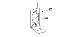
図8は、携帯電話の一例を示した斜視図である。図8において、符号500は携帯電話本体を示し、符号501は上記液晶表示装置を用いた表示部を示している。このような電子機器は、上記実施の形態の液晶表示装置を用いた表示部を備えているので、表示特性が低下することがない、有効画素面積が最大となった電子機器となる。
また、上記の電子機器は、携帯電話に限らず、電子ブック、パーソナルコンピュータ、ディジタルスチルカメラ、液晶テレビ、ビューファインダ型あるいはモニタ直視型のビデオテープレコーダ、カーナビゲーション装置、ページャ、電子手帳、電卓、ワードプロセッサ、ワークステーション、テレビ電話、POS端末、タッチパネルを備えた機器等々の画像表示手段として好適に用いることができ、いずれの電子機器においても視認性に優れた表示が可能になっている。
[Electronics]
Next, specific examples of the electronic apparatus including the liquid crystal display device according to the above embodiment of the present invention will be described.
FIG. 8 is a perspective view showing an example of a mobile phone. In FIG. 8,
In addition, the electronic device is not limited to a mobile phone, but an electronic book, a personal computer, a digital still camera, a liquid crystal television, a viewfinder type or a monitor direct view type video tape recorder, a car navigation device, a pager, an electronic notebook, a calculator, It can be suitably used as an image display means for a word processor, a workstation, a videophone, a POS terminal, a device equipped with a touch panel, etc., and any electronic device can display with excellent visibility.
4…TFD素子(非線形素子)、9…画素電極、13…データ線、32…コンタクトホール、34…層間絶縁膜(層間絶縁層)、35…金属配線、100…液晶表示装置(電気光学装置)
DESCRIPTION OF
Claims (10)
前記基板上に形成されたデータ線と、
前記基板上に形成されるとともに前記データ線と電気的に接続されてなり、第1導電層と第2導電層との間に絶縁層を備える構成の非線形素子であるスイッチング素子と、
前記スイッチング素子から延設してなる配線と、
前記データ線、前記スイッチング素子及び前記配線を覆う形にて前記基板上に形成された層間絶縁層と、
該層間絶縁層上に形成され、前記層間絶縁層に形成されたコンタクトホールを介して、前記配線と電気的に接続されてなる画素電極とを具備することを特徴とする電気光学装置。 A substrate,
Data lines formed on the substrate;
A switching element which is a non-linear element formed on the substrate and electrically connected to the data line and having an insulating layer between the first conductive layer and the second conductive layer;
Wiring extending from the switching element;
An interlayer insulating layer formed on the substrate so as to cover the data line, the switching element and the wiring;
An electro-optical device comprising: a pixel electrode formed on the interlayer insulating layer and electrically connected to the wiring through a contact hole formed in the interlayer insulating layer.
前記基板と前記対向基板との間に、負の誘電異方性を有する液晶が形成されてなることを特徴とする請求項1ないし3のいずれか1項に記載の電気光学装置。 A counter substrate facing the substrate;
4. The electro-optical device according to claim 1, wherein a liquid crystal having negative dielectric anisotropy is formed between the substrate and the counter substrate.
前記対向基板には、前記コンタクトホールと平面的に重なる位置に遮光部が形成されていることを特徴とする請求項1ないし4のいずれか1項に記載の電気光学装置。 A counter substrate facing the substrate;
5. The electro-optical device according to claim 1, wherein the counter substrate is formed with a light-shielding portion at a position overlapping the contact hole in a planar manner.
Priority Applications (1)
| Application Number | Priority Date | Filing Date | Title |
|---|---|---|---|
| JP2004103420A JP2005292223A (en) | 2004-03-31 | 2004-03-31 | Electro-optical device and electronic equipment |
Applications Claiming Priority (1)
| Application Number | Priority Date | Filing Date | Title |
|---|---|---|---|
| JP2004103420A JP2005292223A (en) | 2004-03-31 | 2004-03-31 | Electro-optical device and electronic equipment |
Publications (1)
| Publication Number | Publication Date |
|---|---|
| JP2005292223A true JP2005292223A (en) | 2005-10-20 |
Family
ID=35325259
Family Applications (1)
| Application Number | Title | Priority Date | Filing Date |
|---|---|---|---|
| JP2004103420A Withdrawn JP2005292223A (en) | 2004-03-31 | 2004-03-31 | Electro-optical device and electronic equipment |
Country Status (1)
| Country | Link |
|---|---|
| JP (1) | JP2005292223A (en) |
Cited By (1)
| Publication number | Priority date | Publication date | Assignee | Title |
|---|---|---|---|---|
| JP2017167542A (en) * | 2006-12-26 | 2017-09-21 | 株式会社半導体エネルギー研究所 | Liquid crystal display device |
-
2004
- 2004-03-31 JP JP2004103420A patent/JP2005292223A/en not_active Withdrawn
Cited By (1)
| Publication number | Priority date | Publication date | Assignee | Title |
|---|---|---|---|---|
| JP2017167542A (en) * | 2006-12-26 | 2017-09-21 | 株式会社半導体エネルギー研究所 | Liquid crystal display device |
Similar Documents
| Publication | Publication Date | Title |
|---|---|---|
| JP4645488B2 (en) | Liquid crystal device and electronic device | |
| JP3900123B2 (en) | Liquid crystal display device and electronic device | |
| JP3772842B2 (en) | Liquid crystal device, driving method thereof, and electronic apparatus | |
| US20070279567A1 (en) | Liquid crystal device and electronic apparatus | |
| US7760277B2 (en) | Active matrix LCD panel with first and second alignment layers having respectively plural first and second grooves that extend respectively along ten and one o'clock directions thereon when viewed from above | |
| US20060197898A1 (en) | Liquid crystal device and electronic apparatus | |
| US7460202B2 (en) | Liquid crystal device and electronic apparatus | |
| US7068338B2 (en) | Electro-optical device substrate, electro-optical device, and electronic apparatus | |
| JP5164672B2 (en) | Liquid crystal display device, electronic equipment | |
| US7136116B2 (en) | Liquid crystal display with control electrodes for preventing lateral leak of electric field | |
| JP4453434B2 (en) | Liquid crystal device and electronic device | |
| JP5177984B2 (en) | Liquid crystal device and electronic device | |
| JP4069879B2 (en) | Liquid crystal display device and electronic device | |
| JP4007338B2 (en) | Liquid crystal display device and electronic device | |
| JP2006091486A (en) | Electro-optical device and electronic equipment | |
| JP2004258365A (en) | Electrooptical device and electronic apparatus using it | |
| JP4341617B2 (en) | Liquid crystal display device and electronic device | |
| JP2005316404A (en) | Electro-optical device and electronic apparatus | |
| JP2005292223A (en) | Electro-optical device and electronic equipment | |
| JP5534655B2 (en) | ELECTRO-OPTICAL DEVICE, MANUFACTURING METHOD THEREOF, AND ELECTRONIC DEVICE | |
| JP2005292224A (en) | Electrooptical apparatus and electronic device | |
| JP2007065602A (en) | Liquid crystal device and electronic apparatus | |
| JP2005321501A (en) | Method for manufacturing element substrate and method for manufacturing electrooptical device | |
| JP2006350168A (en) | Liquid crystal device and manufacturing method therefor, and electronic device | |
| JP2009251489A (en) | Liquid crystal device and electronic apparatus |
Legal Events
| Date | Code | Title | Description |
|---|---|---|---|
| A300 | Application deemed to be withdrawn because no request for examination was validly filed |
Free format text: JAPANESE INTERMEDIATE CODE: A300 Effective date: 20070605 |