US7136116B2 - Liquid crystal display with control electrodes for preventing lateral leak of electric field - Google Patents
Liquid crystal display with control electrodes for preventing lateral leak of electric field Download PDFInfo
- Publication number
- US7136116B2 US7136116B2 US10/084,355 US8435502A US7136116B2 US 7136116 B2 US7136116 B2 US 7136116B2 US 8435502 A US8435502 A US 8435502A US 7136116 B2 US7136116 B2 US 7136116B2
- Authority
- US
- United States
- Prior art keywords
- liquid crystal
- crystal display
- control electrode
- electrode
- pixel electrodes
- Prior art date
- Legal status (The legal status is an assumption and is not a legal conclusion. Google has not performed a legal analysis and makes no representation as to the accuracy of the status listed.)
- Expired - Fee Related
Links
- 239000004973 liquid crystal related substance Substances 0.000 title claims abstract description 129
- 230000005684 electric field Effects 0.000 title description 31
- 239000011229 interlayer Substances 0.000 claims abstract description 17
- 239000000758 substrate Substances 0.000 claims description 53
- 239000010408 film Substances 0.000 claims description 41
- 239000010410 layer Substances 0.000 claims description 33
- 239000011159 matrix material Substances 0.000 claims description 24
- 230000008878 coupling Effects 0.000 claims description 8
- 238000010168 coupling process Methods 0.000 claims description 8
- 238000005859 coupling reaction Methods 0.000 claims description 8
- 229910052751 metal Inorganic materials 0.000 claims description 8
- 239000002184 metal Substances 0.000 claims description 8
- 239000002356 single layer Substances 0.000 claims description 3
- 239000010409 thin film Substances 0.000 description 15
- 238000000034 method Methods 0.000 description 11
- 238000004519 manufacturing process Methods 0.000 description 8
- 239000004925 Acrylic resin Substances 0.000 description 5
- 229920000178 Acrylic resin Polymers 0.000 description 5
- 238000010586 diagram Methods 0.000 description 4
- 238000002161 passivation Methods 0.000 description 4
- VYZAMTAEIAYCRO-UHFFFAOYSA-N Chromium Chemical compound [Cr] VYZAMTAEIAYCRO-UHFFFAOYSA-N 0.000 description 3
- RTAQQCXQSZGOHL-UHFFFAOYSA-N Titanium Chemical compound [Ti] RTAQQCXQSZGOHL-UHFFFAOYSA-N 0.000 description 3
- 229910052804 chromium Inorganic materials 0.000 description 3
- 239000011651 chromium Substances 0.000 description 3
- 238000005516 engineering process Methods 0.000 description 3
- 238000012986 modification Methods 0.000 description 3
- 230000004048 modification Effects 0.000 description 3
- 229910052719 titanium Inorganic materials 0.000 description 3
- 239000010936 titanium Substances 0.000 description 3
- ZOKXTWBITQBERF-UHFFFAOYSA-N Molybdenum Chemical compound [Mo] ZOKXTWBITQBERF-UHFFFAOYSA-N 0.000 description 2
- 229910052782 aluminium Inorganic materials 0.000 description 2
- XAGFODPZIPBFFR-UHFFFAOYSA-N aluminium Chemical compound [Al] XAGFODPZIPBFFR-UHFFFAOYSA-N 0.000 description 2
- 239000011521 glass Substances 0.000 description 2
- AMGQUBHHOARCQH-UHFFFAOYSA-N indium;oxotin Chemical compound [In].[Sn]=O AMGQUBHHOARCQH-UHFFFAOYSA-N 0.000 description 2
- 229910052750 molybdenum Inorganic materials 0.000 description 2
- 239000011733 molybdenum Substances 0.000 description 2
- 125000006850 spacer group Chemical group 0.000 description 2
- 238000004528 spin coating Methods 0.000 description 2
- 229910052581 Si3N4 Inorganic materials 0.000 description 1
- NIXOWILDQLNWCW-UHFFFAOYSA-N acrylic acid group Chemical group C(C=C)(=O)O NIXOWILDQLNWCW-UHFFFAOYSA-N 0.000 description 1
- 230000005540 biological transmission Effects 0.000 description 1
- 238000004891 communication Methods 0.000 description 1
- 239000000463 material Substances 0.000 description 1
- 238000000059 patterning Methods 0.000 description 1
- 238000000206 photolithography Methods 0.000 description 1
- 230000000630 rising effect Effects 0.000 description 1
- HQVNEWCFYHHQES-UHFFFAOYSA-N silicon nitride Chemical compound N12[Si]34N5[Si]62N3[Si]51N64 HQVNEWCFYHHQES-UHFFFAOYSA-N 0.000 description 1
Images


Classifications
-
- G—PHYSICS
- G02—OPTICS
- G02F—OPTICAL DEVICES OR ARRANGEMENTS FOR THE CONTROL OF LIGHT BY MODIFICATION OF THE OPTICAL PROPERTIES OF THE MEDIA OF THE ELEMENTS INVOLVED THEREIN; NON-LINEAR OPTICS; FREQUENCY-CHANGING OF LIGHT; OPTICAL LOGIC ELEMENTS; OPTICAL ANALOGUE/DIGITAL CONVERTERS
- G02F1/00—Devices or arrangements for the control of the intensity, colour, phase, polarisation or direction of light arriving from an independent light source, e.g. switching, gating or modulating; Non-linear optics
- G02F1/01—Devices or arrangements for the control of the intensity, colour, phase, polarisation or direction of light arriving from an independent light source, e.g. switching, gating or modulating; Non-linear optics for the control of the intensity, phase, polarisation or colour
- G02F1/13—Devices or arrangements for the control of the intensity, colour, phase, polarisation or direction of light arriving from an independent light source, e.g. switching, gating or modulating; Non-linear optics for the control of the intensity, phase, polarisation or colour based on liquid crystals, e.g. single liquid crystal display cells
- G02F1/133—Constructional arrangements; Operation of liquid crystal cells; Circuit arrangements
- G02F1/1333—Constructional arrangements; Manufacturing methods
- G02F1/1343—Electrodes
- G02F1/134309—Electrodes characterised by their geometrical arrangement
- G02F1/134336—Matrix
-
- G—PHYSICS
- G02—OPTICS
- G02F—OPTICAL DEVICES OR ARRANGEMENTS FOR THE CONTROL OF LIGHT BY MODIFICATION OF THE OPTICAL PROPERTIES OF THE MEDIA OF THE ELEMENTS INVOLVED THEREIN; NON-LINEAR OPTICS; FREQUENCY-CHANGING OF LIGHT; OPTICAL LOGIC ELEMENTS; OPTICAL ANALOGUE/DIGITAL CONVERTERS
- G02F1/00—Devices or arrangements for the control of the intensity, colour, phase, polarisation or direction of light arriving from an independent light source, e.g. switching, gating or modulating; Non-linear optics
- G02F1/01—Devices or arrangements for the control of the intensity, colour, phase, polarisation or direction of light arriving from an independent light source, e.g. switching, gating or modulating; Non-linear optics for the control of the intensity, phase, polarisation or colour
- G02F1/13—Devices or arrangements for the control of the intensity, colour, phase, polarisation or direction of light arriving from an independent light source, e.g. switching, gating or modulating; Non-linear optics for the control of the intensity, phase, polarisation or colour based on liquid crystals, e.g. single liquid crystal display cells
- G02F1/133—Constructional arrangements; Operation of liquid crystal cells; Circuit arrangements
- G02F1/136—Liquid crystal cells structurally associated with a semi-conducting layer or substrate, e.g. cells forming part of an integrated circuit
- G02F1/1362—Active matrix addressed cells
- G02F1/136218—Shield electrodes
Definitions
- the present invention relates generally to a liquid crystal display used, for example, in a display of a computer and the like. More particularly, the present invention relates to a liquid crystal display which has switching elements each comprising a thin film transistor (TFT) and in which lateral leak of electric field caused by the potential difference between gate lines and pixel electrodes can be effectively prevented.
- TFT thin film transistor
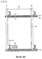
- FIG. 9 and FIG. 10 illustrate a liquid crystal display described in Japanese patent laid-open publication No. 10-221715.
- FIG. 9 is a plan view showing a portion of an active matrix substrate in such liquid crystal display.
- FIG. 10 is a cross sectional view taken along the line A—A of FIG. 9 .
- an active matrix substrate 50 comprises an insulating substrate 51 made, for example, of glass and the like, a gate insulating film 52 formed on the insulating substrate 51 , a passivation film 53 formed on the gate insulating film 52 , an interlayer insulating film 54 formed on the passivation film 53 , and pixel electrodes 55 which are formed in a matrix on the interlayer insulating film 54 .
- gate lines 56 and data lines 57 are disposed on the periphery of each of the pixel electrode 55 .
- the gate lines 56 and the data lines 57 are perpendicular to each other, and surround each of the pixel electrodes 55 .
- each of the gate lines 56 is formed on the insulating substrate 51
- each of the data lines 57 (not shown in FIG. 10 ) is formed on the gate insulating film 52 .
- a thin film transistor (TFT) 58 as a switching element is disposed in the proximity of each of the intersections between the gate lines 56 and the data lines 57 .
- the thin film transistor 58 is electrically coupled to the pixel electrode 55 via a contact hole 59 which is formed in the interlayer insulating film 54 .
- a gate electrode of the thin film transistor 58 is coupled with the gate line 56 , and the thin film transistor 58 is driven and controlled by a signal applied to the gate electrode via the gate line 56 . Also, a drain electrode of the thin film transistor 58 is coupled with the data line 57 , and a data signal is inputted to the drain electrode via the data line 57 .
- a control electrode 60 is formed on the interlayer insulating film 54 , between adjacent pixel electrodes 55 and over the gate line 56 .
- the control electrode 60 is formed in the same layer as that of the pixel electrodes 55 .
- FIG. 10 also shows an opposing substrate 64 which opposes to the active matrix substrate 50 .
- the opposing substrate 64 comprises an insulating substrate 61 , a color filter 62 formed on the insulating substrate 61 , and an opposing electrode 63 formed on the color filter 62 .
- the opposing substrate 64 is disposed such that the opposing electrode 63 and the pixel electrodes 55 oppose to each other.
- an alignment layer (not shown in the drawing). Also, there is provided a liquid crystal layer 65 which is held between the alignment layers on the active matrix substrate 50 and on the opposing substrate 64 . Also, spacers (not shown in the drawing) are disposed between the active matrix substrate 50 and the opposing substrate 64 to keep a predetermined thickness of the liquid crystal layer 65 . Further, there is formed a seal (not shown in the drawing) around the liquid crystal layer 65 for preventing liquid crystal molecules from leaking outside.
- control electrode 60 is disposed between adjacent pixel electrodes 55 .
- the control electrode 60 is provided to avoid occurrence of so-called reverse tilt.
- the reverse tilt occurs when an electric field caused by the potential difference between the gate line 56 and the pixel electrodes 55 intrudes into the liquid crystal layer 65 , and alignment direction of liquid crystal molecules partly differs from a predetermined direction.
- control electrodes 60 in the same layer as that of the pixel electrodes 55 .
- the space between mutually adjacent pixel electrodes 55 is not large and, therefore, the width of the control electrode 60 can not be so large. Further, when the control electrode 60 is to be formed in such narrow space between adjacent pixel electrodes 55 , there is a high possibility that the control electrode 60 contacts one or both of the adjacent pixel electrodes 55 .
- Such lateral leak of electric field 68 causes reverse tilt of liquid crystal molecules in the liquid crystal layer 65 , and as a result causes disclination.
- a liquid crystal display comprising: a plurality of gate lines disposed parallel to each other; a plurality of data lines disposed parallel to each other and perpendicularly to the plurality of gate lines; switching elements each disposed in the proximity of one of intersections between the plurality of gate lines and the plurality of data lines; a plurality of pixel electrodes disposed over the gate lines and the data lines via an interlayer insulating film, wherein, when viewed from upside, that is, from the side of a gap between adjacent pixel electrodes toward the side of the gate line, the gap between adjacent pixel electrodes at least partially overlaps with the gate line; and a plurality of control electrodes each disposed under the gap between adjacent pixel electrodes and over the gate line, wherein, when viewed from upside through the gap, the control electrode covers the gate line.
- liquid crystal display when viewed from the gap between the adjacent pixel electrodes, the gate line is wholly covered by the control electrode. Therefore, the electric field produced by the potential difference between the gate line and the pixel electrodes is completely shielded by the control electrode. That is, a phenomenon in which the electric field leaks through the gap between the pixel electrodes and extends laterally along the pixel electrodes into the liquid crystal layer, i.e., the so-called lateral leak of electric field, can be effectively avoided.
- control electrode when viewed from upside, the control electrode at least overlaps with the gap between adjacent pixel electrodes in width direction.
- control electrode when viewed from upside, the control electrode at least overlaps with an area in which the gate line and the gap between adjacent pixel electrodes overlap.
- control electrode overlaps with the gate line and with the gap between adjacent pixel electrodes.
- control electrode has the same potential voltage as that of a source electrode of the switching element.
- control electrode is formed in the same layer as that of a source electrode of the switching element.
- control electrode and the source electrode may be formed on mutually different layers. However, by forming the control electrode and the source electrode on the same layer, it is possible to form the control electrode and the source electrode in the same manufacturing process and to simplify the manufacturing process, so that productivity of the liquid crystal display can be improved.
- control electrode is formed integrally with a source electrode of the switching element.
- control electrode and the source electrode may be formed as separate pieces. However, by forming the control electrode and the source electrode integrally, it is possible to form the control electrode and the source electrode in the same manufacturing process and to simplify the manufacturing process, so that productivity of the liquid crystal display can be improved.
- control electrode has a single layer structure comprising metal or ITO.
- control electrode has a multi-layer structure, each layer thereof comprising metal or ITO.
- the interlayer insulating film comprises an organic film.
- the liquid crystal display has a COT structure.
- the liquid crystal display is a reflection type liquid crystal display.
- control electrode and a source electrode of the switching element are coupled via an extended portion of the source electrode, and a contact hole for coupling the control electrode and the pixel electrode is provided on the extended portion.
- a contact hole for coupling the control electrode and the pixel electrode is provided on the control electrode.
- the contact hole By forming the contact hole on the control electrode, it is possible to improve an aperture ratio by the amount corresponding to the area of the contact hole, when compared with the case the contact hole is formed on the extended portion.
- an electronic equipment which includes the above-mentioned liquid crystal display, in a display portion of the electronic equipment.
- a liquid crystal display comprising: an active matrix substrate; an opposing substrate which is opposed to the active matrix substrate; and a liquid crystal layer interposed between the active matrix substrate and the opposing substrate; wherein the active matrix substrate comprises: a plurality of gate lines which are disposed on an insulating substrate and which are disposed parallel to each other; a plurality of data lines which are disposed on the plurality of gate lines via a gate insulating film and which are disposed parallel to each other and perpendicularly to the plurality of gate lines; switching elements each disposed in the proximity of one of intersections between the plurality of gate lines and the plurality of data lines; a plurality of pixel electrodes disposed over the gate lines and the data lines via an interlayer insulating film, wherein, when viewed from upside, that is, from the side of a gap between adjacent pixel electrodes toward the side of the gate line, the gap between adjacent pixel electrodes at least partially overlaps with the gate line; and a plurality of
- control electrode is formed integrally with a source electrode of the switching element.
- control electrode and a source electrode of the switching element are coupled via an extended portion of the source electrode, and a contact hole for coupling the control electrode and the pixel electrode is provided on the extended portion.
- a contact hole for coupling the control electrode and the pixel electrode is provided on the control electrode.
- FIG. 1 is a plan view showing a portion of an active matrix substrate in a liquid crystal display according to a first embodiment of the present invention
- FIG. 2 is a partial cross sectional view taken along the line B—B of FIG. 1 ;
- FIG. 3 is a partial cross sectional view showing a first example of a locational relationship among a gate line, a gap between pixel electrodes and a control electrode;
- FIG. 4 is a partial cross sectional view showing a second example of a locational relationship among a gate line, a gap between pixel electrodes and a control electrode;
- FIG. 5 is a partial cross sectional view showing a third example of a locational relationship among a gate line, a gap between pixel electrodes and a control electrode;
- FIG. 6 is a partial cross sectional view showing a fourth example of a locational relationship among a gate line, a gap between pixel electrodes and a control electrode;
- FIG. 7 is a block diagram showing an example of an electronic equipment to which a liquid crystal display according to the present invention is applied.
- FIG. 8 is a block diagram showing another example of an electronic equipment to which a liquid crystal display according to the present invention is applied.
- FIG. 9 is a plan view showing a portion of an active matrix substrate in a conventional liquid crystal display.
- FIG. 10 is a partial cross sectional view taken along the line A—A of FIG. 9 .
- FIG. 1 is a plan view showing a portion of an active matrix substrate in the liquid crystal display according to the first embodiment of the present invention.
- FIG. 2 is a partial cross sectional view taken along the line B—B of FIG. 1 .
- an active matrix substrate 10 comprises an insulating substrate 11 made, for example, of glass and the like, a gate insulating film 12 formed on the insulating substrate 11 , a control electrode 20 formed on the gate insulating film 12 , a passivation film 13 which is formed on the gate insulating film 12 and which covers the control electrode 20 , an interlayer insulating film 14 formed on the passivation film 13 , and pixel electrodes 15 which are formed in a matrix on the interlayer insulating film 14 .
- gate lines 16 and data lines 17 are disposed on the periphery of each of the pixel electrodes 15 .
- the gate lines 16 and the data lines 17 are perpendicular to each other, and surround each of the pixel electrodes 15 .
- the gate line 16 is formed on the insulating substrate 11
- the data line 17 (not shown in FIG. 2 ) is formed on the gate insulating film 12 .
- a thin film transistor (TFT) 18 as a switching element is disposed in the proximity of each of the intersections between the gate lines 16 and the data lines 17 .
- the thin film transistor 18 is electrically coupled to the pixel electrode 15 via a contact hole 19 which is formed in the interlayer insulating film 14 and which is explained in detail later.
- a gate electrode of the thin film transistor 18 is coupled with the gate line 16 , and the thin film transistor 18 is driven and controlled by a signal applied to the gate electrode via the gate line 16 . Also, a drain electrode of the thin film transistor 18 is coupled with the data line 17 , and a data signal is inputted to the drain electrode via the data line 17 .
- the opposing substrate 24 which opposes to the active matrix substrate 10 .
- the opposing substrate 24 comprises an insulating substrate 21 , a color filter 22 formed on the insulating substrate 21 , and an opposing electrode 23 formed on the color filter 22 .
- the opposing substrate 24 is disposed such that the opposing electrode 23 and the pixel electrodes 15 oppose to each other.
- an alignment layer (not shown in the drawing). Also, there is provided a liquid crystal layer 25 which is held between the alignment layers on the active matrix substrate 10 and on the opposing substrate 24 . Also, spacers (not shown in the drawing) are disposed between the active matrix substrate 10 and the opposing substrate 24 to keep a predetermined thickness of the liquid crystal layer 25 . Further, there is formed a seal (not shown in the drawing) around the liquid crystal layer 25 for preventing liquid crystal molecules from leaking outside.
- each pixel electrode 15 comprises a transparent conductive film such as indium tin oxide (ITO) film and the like.
- each pixel electrode 15 comprises a metal film such as aluminum film and the like.
- the gate lines 16 and the data lines 17 are made, for example, of metal such as aluminum, titanium and the like.
- Each of the control electrodes 20 is formed, for example, as a single layer structure made of metal such as chromium, molybdenum, titanium or the like.
- the interlayer insulating film 14 in this embodiment is an organic film, and comprises a photosensitive acrylic resin.
- the photosensitive acrylic resin has a relative dielectric constant in a range approximately from 3.4 to 3.5.
- the relative dielectric constant of the photosensitive acrylic resin is very low when compared with that of an inorganic film.
- a relative dielectric constant of a silicon nitride is approximately 8.
- the photosensitive acrylic resin has high transparency, and can be easily applied by spin coating to form a relatively thick thin film. Therefore, it is possible to easily lower the capacitance between the gate lines 16 and the pixel electrodes 15 and the capacitance between the data lines 17 and the pixel electrodes 15 . As a result, it becomes possible to mitigate an influence of the cross talk on display operation caused by the capacitance component between the gate lines 16 and the pixel electrodes 15 and the capacitance component between the data lines 17 and the pixel electrodes 15 .
- the photosensitive acrylic resin By using the photosensitive acrylic resin, it is possible to easily form a relatively thick thin film having a thickness of several microns or so, for example, by spin coating. Also, when patterning the photosensitive acrylic film, a photolithography process is not required and, therefore, productivity of the liquid crystal display can be improved.
- control electrode 20 which is formed on the gate insulating film 12 , wholly covers the gate line 16 and also wholly covers the gap 26 , when viewed from upside of FIG. 2 .
- the source electrode 18 a of the thin film transistor 18 has an extended portion 18 b which traverses the pixel electrode 15 a and which extends to the control electrode 20 . Therefore, the control electrode 20 is integrally formed with the source electrode 18 a via the extended portion 18 b.
- the pixel electrode 15 a is coupled with the control electrode 20 and, therefore, with the source electrode 18 a of the thin film transistor 18 .
- liquid crystal display according to the first embodiment can be driven by any of the driving methods such as a data line potential inverting method, a gate line potential inverting method, and a dot potential inverting method.
- the data line potential inverting method is a driving method in which polarity of a signal voltage of each pixel electrode is inverted every data line to which the pixel electrode is coupled.
- the gate line potential inverting method is a driving method in which polarity of a signal voltage of each pixel electrode is inverted every gate line to which the pixel electrode is coupled.
- the dot potential inverting method is a driving method in which polarities of signal voltages of mutually adjacent pixels differ from each other.
- the control electrode 20 is formed such that it wholly covers both the gate line 16 and the gap 26 between adjacent pixel electrodes. Therefore, the electric field produced by the potential difference between the gate line 16 and the pixel electrodes 15 is completely shielded by the control electrode 20 . That is, a phenomenon in which the electric field leaks through the gap 26 and extends laterally along the pixel electrodes 15 into the liquid crystal layer 25 , i.e., the so-called lateral leak of electric field, can be effectively avoided.
- the structure of the liquid crystal display according to the present embodiment is not limited to the above-mentioned structure, but can be modified into various structures as mentioned below.
- the control electrode 20 when viewed from the side of the opposing substrate, i.e., from upside, the control electrode 20 is formed such that the control electrode 20 completely overlaps with the gate line 16 and the gap 26 between the pixel electrodes 15 a and 15 b , as shown in FIG. 2 .
- the structure of the control electrode 20 is not limited to such structure.
- the width of the gate line 16 may be larger than the width of the gap 26 , and, when viewed from upside, the gap 26 may be wholly contained in the gate line 16 .
- the control electrode 20 when viewed from upside, the control electrode 20 may be formed such that the control electrode 20 at least overlaps the gap 26 in width direction. It is not always necessary to form the control electrode 20 such that the control electrode 20 wholly covers the gate line 16 . Even when the control electrode 20 does not cover the gate line 16 completely, if the gap 26 is wholly covered by the control electrode 20 , it is possible to avoid occurrence of the lateral leak of electric field 68 like that of the conventional liquid crystal display shown in FIG. 10 .
- the width of the gate line 16 may be smaller than the width of the gap 26 , and, when viewed from upside, the gate line 16 may be wholly contained in the gap 26 .
- the control electrode 20 when viewed from upside, the control electrode 20 may be formed such that the control electrode 20 at least overlaps the gate line 16 in width direction. It is not always necessary to form the control electrode 20 such that the control electrode 20 wholly covers the gap 26 . Even when the control electrode 20 does not cover the gap 26 completely, if the gate line 16 is wholly covered by the control electrode 20 , it is possible to avoid occurrence of the lateral leak of electric field 68 in the conventional liquid crystal display shown in FIG. 10 .
- the gate line 16 when viewed from upside, the gate line 16 may be partially contained in the gap 26 , and a gap may exist between the pixel electrode 15 b and the gate line 16 .
- the gate line 16 when viewed from upside, the gate line 16 may be partially contained in the gap 26 , and a gap may exist between the pixel electrode 15 a and the gate line 16 .
- the control electrode 20 may be formed such that the control electrode 20 at least overlaps the gate line 16 in width direction or such that the control electrode 20 at least overlaps the gap 26 in width direction. It is not always necessary to form the control electrode 20 such that the control electrode 20 also completely overlaps the gap 26 and the gate line 16 , in respective cases. Even when the control electrode 20 does not cover both the gap 26 and the gate line 16 completely, if the gate line 16 or the gap 26 is wholly covered by the control electrode 20 in width direction, it is possible to avoid occurrence of the lateral leak of electric field 68 in the conventional liquid crystal display shown in FIG. 10 .
- control electrode 20 is formed integrally with the source electrode 18 a via the extended portion 18 b .
- control electrode 20 and the source electrode 18 a are formed separately, without forming the extended portion 18 b .
- the control electrode 20 and the source electrode 18 a are formed on the same layer.
- control electrode 20 and the source electrode 18 a are formed as separate pieces, it is preferable that that the potential of the control electrode 20 and the potential of the source electrode 18 a are made equal to each other.
- control electrode 20 is made of metal such as chromium and the like.
- ITO indium tin oxide
- control electrode 20 it is also possible to form the control electrode 20 as a multi-layer structure which is made of two or more materials selected from a group consisting of chromium, molybdenum, titanium and ITO.
- the liquid crystal display is formed as a liquid crystal display having an organic interlayer film structure.
- the liquid crystal display according to the present invention can be formed as a liquid crystal display having a COT structure, a reflection type liquid crystal display or the like.
- the contact hole 19 is formed at a location of the extended portion 18 b of the source electrode 18 a .
- By forming the contact hole 19 on the control electrode 20 it is possible to improve an aperture ratio by the amount corresponding to the area of the contact hole 19 , when compared with the case the contact hole 19 is formed on the extended portion 18 b.
- liquid crystal displays of a type in which a direction of aligned liquid crystal molecules, i.e., a director, is rotated in a plane perpendicular to the substrate to perform display operation, and of a type in which a director is rotated in a plane parallel to the substrate to perform display operation.
- a typical example of a liquid crystal display of the former type is a liquid crystal display of TN (Twisted Nematic) mode
- a liquid crystal display of the latter type is called a liquid crystal display of IPS (In-Plane Switching) mode or lateral electric field mode.
- IPS In-Plane Switching
- a viewer sees the screen of the liquid crystal display only in the direction of short axis of liquid crystal molecules even if he changed a viewpoint. Therefore, viewing angle characteristics do not depend on a rising angle of liquid crystal molecules, so that wider viewing angle characteristics can be attained than those of the liquid crystal display of TN mode.
- liquid crystal display according to the first embodiment mentioned above it is possible to select any of the liquid crystal display of TN mode and the liquid crystal display of IPS mode.
- the liquid crystal display according to the first embodiment mentioned above and variation thereof can be applied to various electronic equipment. An explanation will now be made on examples of such electronic equipment.
- FIG. 7 is a block diagram of a portable information terminal 250 to which the above-mentioned liquid crystal display according to the first embodiment is applied.
- the above-mentioned liquid crystal display according to the first embodiment is used as a component of a liquid crystal display panel 265 , in this portable information terminal 250 .
- the portable information terminal 250 comprises a display portion 268 , a control portion 269 , a memory portion 271 , a communicating circuit portion 272 , an input portion 273 and a power source 274 .
- the display portion 268 includes the liquid crystal display panel 265 , a back light generating means 266 , and an image signal processing portion 267 .
- the image signal processing portion 267 generates various signals required for driving the liquid crystal display panel 265 based on an input signal received from the control portion 269 and the like.
- the control portion 269 comprises a microprocessor and the like, generates various control signals for components of the portable information terminal 250 and controls an operation thereof.
- the memory portion 271 stores a program executed by the control portion 269 and various data.
- the communicating circuit portion 272 performs data communication and the like.
- the input portion 273 comprises, for example, a key board or a pointer.
- the power source 274 comprises, for example, a rechargeable battery and supplies electric power to various components of the portable information terminal 250 .
- liquid crystal display panel 265 which includes the liquid crystal display according to the first embodiment of the present invention, it is possible to improve display quality of various images, characters and the like in the display portion 268 .
- the liquid crystal display panel 265 which includes the liquid crystal display according to the first embodiment of the present invention can be applied to a display monitor apparatus, for example, of a portable type personal computer, a notebook type personal computer or a desktop type personal computer.
- FIG. 8 is a block diagram of a portable telephone 275 to which the above-mentioned liquid crystal display according to the first embodiment is applied.
- the portable telephone 275 comprises a display portion 276 , a control portion 277 , a memory portion 278 , a receiving circuit portion or receiver 279 , a transmitting circuit portion or transmitter 281 , an input portion 282 and a power source 283 .
- the display portion 276 includes the liquid crystal display panel 265 , a back light generating means 266 , and an image signal processing portion 267 .
- the image signal processing portion 267 generates various signals required for driving the liquid crystal display panel 265 based on an input signal received from the control portion 277 and the like.
- the control portion 277 comprises a microprocessor and the like, generates various control signals for components of the portable telephone 275 and controls an operation thereof.
- the memory portion 278 stores a program executed by the control portion 277 and various data.
- the receiving circuit portion 279 receives a radio signal and supplies received information to the control portion 277 .
- the transmitting circuit portion 281 receives information from the control portion 277 and transmits a radio signal.
- the input portion 282 comprises, for example, a key board or a pointer.
- the power source 283 comprises, for example, a rechargeable battery and supplies electric power to various components of the portable telephone 275 .
- liquid crystal display panel 265 which includes the liquid crystal display according to the first embodiment of the present invention, it is possible to improve display quality of various images, characters and the like in the display portion 276 .
- the control electrode is formed such that the control electrode covers at least the gate line 16 in the gap portion between the pixel electrodes. Therefore, the electric field produced by the potential difference between the gate line and the pixel electrodes is completely shielded by the control electrode. That is, a phenomenon in which the electric field leaks through the gap between the pixel electrodes and extends laterally along the pixel electrodes into the liquid crystal layer, i.e., the so-called lateral leak of electric field, can be effectively avoided.
- the pixel electrode and the control electrode are coupled with each other via the contact hole, an auxiliary capacitance is formed between the control electrode and the gate line via the gate insulating film interposed therebetween. Therefore, according to the structure of the present invention, it is possible to increase the storage capacitance of the liquid crystal display.
Landscapes
- Physics & Mathematics (AREA)
- Nonlinear Science (AREA)
- Mathematical Physics (AREA)
- Chemical & Material Sciences (AREA)
- Crystallography & Structural Chemistry (AREA)
- General Physics & Mathematics (AREA)
- Optics & Photonics (AREA)
- Geometry (AREA)
- Liquid Crystal (AREA)
- Engineering & Computer Science (AREA)
- Microelectronics & Electronic Packaging (AREA)
- Devices For Indicating Variable Information By Combining Individual Elements (AREA)
- Internal Circuitry In Semiconductor Integrated Circuit Devices (AREA)
- Thin Film Transistor (AREA)
Abstract
Description
Claims (22)
Applications Claiming Priority (2)
| Application Number | Priority Date | Filing Date | Title |
|---|---|---|---|
| JP2001-055191 | 2001-02-28 | ||
| JP2001055191A JP2002258320A (en) | 2001-02-28 | 2001-02-28 | Liquid crystal display device |
Publications (2)
| Publication Number | Publication Date |
|---|---|
| US20020118331A1 US20020118331A1 (en) | 2002-08-29 |
| US7136116B2 true US7136116B2 (en) | 2006-11-14 |
Family
ID=18915407
Family Applications (1)
| Application Number | Title | Priority Date | Filing Date |
|---|---|---|---|
| US10/084,355 Expired - Fee Related US7136116B2 (en) | 2001-02-28 | 2002-02-28 | Liquid crystal display with control electrodes for preventing lateral leak of electric field |
Country Status (4)
| Country | Link |
|---|---|
| US (1) | US7136116B2 (en) |
| JP (1) | JP2002258320A (en) |
| KR (1) | KR100498254B1 (en) |
| TW (1) | TW583482B (en) |
Cited By (6)
| Publication number | Priority date | Publication date | Assignee | Title |
|---|---|---|---|---|
| US20060023137A1 (en) * | 2004-07-28 | 2006-02-02 | Fujitsu Display Technologies Corporation | Liquid crystal display device and method of preventing image sticking thereon |
| US20070007525A1 (en) * | 2005-07-09 | 2007-01-11 | Samsung Electronics Co., Ltd. | Liquid crystal display with wide viewing angle |
| US20070030432A1 (en) * | 2005-08-08 | 2007-02-08 | Innolux Display Corp. | In plane switching liquid crystal display with storage capacitor corresponding to shielding metal line |
| US20070105286A1 (en) * | 2005-10-17 | 2007-05-10 | Samsung Electronics Co., Ltd | Thin film transistor array panel and manufacturing method thereof |
| US20090086135A1 (en) * | 2007-09-27 | 2009-04-02 | Hitachi Displays, Ltd. | Liquid Crystal Display Device |
| US20110025923A1 (en) * | 2008-04-25 | 2011-02-03 | Sharp Kabushiki Kaisha | Liquid crystal display device and television receiver |
Families Citing this family (8)
| Publication number | Priority date | Publication date | Assignee | Title |
|---|---|---|---|---|
| TWI227460B (en) | 2002-09-30 | 2005-02-01 | Seiko Epson Corp | Active matrix type optoelectronic device and electronic machine |
| TWI223730B (en) * | 2003-07-14 | 2004-11-11 | Au Optronics Corp | Optically self-compensated birefringence liquid crystal display |
| KR101061842B1 (en) * | 2003-09-19 | 2011-09-02 | 삼성전자주식회사 | Multi-domain liquid crystal display device and thin film transistor display panel thereof |
| US20050231447A1 (en) * | 2004-04-14 | 2005-10-20 | Shuo-Hsiu Hu | Pixel arrangement in a display system |
| US7956972B2 (en) * | 2004-09-14 | 2011-06-07 | Himax Technologies Limited | Liquid crystal on silicon display panel with reducing fringe effect |
| KR20070059293A (en) * | 2005-12-06 | 2007-06-12 | 삼성전자주식회사 | Liquid crystal display device, display panel for same and method of manufacturing same |
| TWI356263B (en) | 2007-11-30 | 2012-01-11 | Hannstar Display Corp | Liquid crystal display with high aperture ratio |
| RU2475791C1 (en) | 2009-02-13 | 2013-02-20 | Шарп Кабусики Кайся | Matrix substrate, liquid crystal display device, electronic device |
Citations (12)
| Publication number | Priority date | Publication date | Assignee | Title |
|---|---|---|---|---|
| JPH04319920A (en) | 1991-04-19 | 1992-11-10 | Sharp Corp | Active matrix liquid crystal display device |
| JPH05273584A (en) | 1992-03-26 | 1993-10-22 | Fujitsu Ltd | LCD display panel |
| JPH09152625A (en) | 1995-08-11 | 1997-06-10 | Sharp Corp | Transmissive liquid crystal display device and manufacturing method thereof |
| US5682211A (en) * | 1994-04-28 | 1997-10-28 | Xerox Corporation | Integrated dark matrix for an active matrix liquid crystal display with pixel electrodes overlapping gate data lines |
| JPH1078593A (en) | 1996-09-04 | 1998-03-24 | Semiconductor Energy Lab Co Ltd | Display device |
| JPH10221715A (en) | 1997-02-10 | 1998-08-21 | Sharp Corp | Liquid crystal display device and driving method thereof |
| JPH11109417A (en) | 1997-10-07 | 1999-04-23 | Sharp Corp | Active matrix type liquid crystal display |
| US5946065A (en) * | 1995-10-31 | 1999-08-31 | Sharp Kabushiki Kaisha | Transmission type LCD with an organic interlayer insulating film having a plurality of microscopic hollows |
| US5986724A (en) * | 1996-03-01 | 1999-11-16 | Kabushiki Kaisha Toshiba | Liquid crystal display with liquid crystal layer and ferroelectric layer connected to drain of TFT |
| US6219118B1 (en) | 1995-05-08 | 2001-04-17 | Semiconductor Energy Laboratory Co., Ltd. | LCD with shield film formed at overlapping portion of bus lines and pixel electrode |
| JP2001215529A (en) | 2000-02-03 | 2001-08-10 | Matsushita Electric Ind Co Ltd | Reflective liquid crystal display |
| US6445435B1 (en) * | 1998-01-23 | 2002-09-03 | Lg. Philips Lcd Co., Ltd. | In-plane switching mode liquid cystal display device having common electrode on passivation layer |
Family Cites Families (6)
| Publication number | Priority date | Publication date | Assignee | Title |
|---|---|---|---|---|
| JP2702319B2 (en) * | 1991-07-25 | 1998-01-21 | シャープ株式会社 | Active matrix substrate |
| JP2777545B2 (en) * | 1994-12-05 | 1998-07-16 | 株式会社フロンテック | Active matrix liquid crystal display |
| JP3739523B2 (en) * | 1997-04-16 | 2006-01-25 | 富士写真フイルム株式会社 | Reflective two-dimensional matrix spatial light modulator |
| JP2000002889A (en) * | 1998-06-16 | 2000-01-07 | Mitsubishi Electric Corp | Liquid crystal display |
| JP3125872B2 (en) * | 1998-09-14 | 2001-01-22 | 日本電気株式会社 | Active matrix type liquid crystal display |
| JP3049022B2 (en) * | 1998-11-13 | 2000-06-05 | 鹿児島日本電気株式会社 | Liquid crystal display |
-
2001
- 2001-02-28 JP JP2001055191A patent/JP2002258320A/en active Pending
-
2002
- 2002-02-26 TW TW091103514A patent/TW583482B/en not_active IP Right Cessation
- 2002-02-27 KR KR10-2002-0010678A patent/KR100498254B1/en not_active Expired - Fee Related
- 2002-02-28 US US10/084,355 patent/US7136116B2/en not_active Expired - Fee Related
Patent Citations (12)
| Publication number | Priority date | Publication date | Assignee | Title |
|---|---|---|---|---|
| JPH04319920A (en) | 1991-04-19 | 1992-11-10 | Sharp Corp | Active matrix liquid crystal display device |
| JPH05273584A (en) | 1992-03-26 | 1993-10-22 | Fujitsu Ltd | LCD display panel |
| US5682211A (en) * | 1994-04-28 | 1997-10-28 | Xerox Corporation | Integrated dark matrix for an active matrix liquid crystal display with pixel electrodes overlapping gate data lines |
| US6219118B1 (en) | 1995-05-08 | 2001-04-17 | Semiconductor Energy Laboratory Co., Ltd. | LCD with shield film formed at overlapping portion of bus lines and pixel electrode |
| JPH09152625A (en) | 1995-08-11 | 1997-06-10 | Sharp Corp | Transmissive liquid crystal display device and manufacturing method thereof |
| US5946065A (en) * | 1995-10-31 | 1999-08-31 | Sharp Kabushiki Kaisha | Transmission type LCD with an organic interlayer insulating film having a plurality of microscopic hollows |
| US5986724A (en) * | 1996-03-01 | 1999-11-16 | Kabushiki Kaisha Toshiba | Liquid crystal display with liquid crystal layer and ferroelectric layer connected to drain of TFT |
| JPH1078593A (en) | 1996-09-04 | 1998-03-24 | Semiconductor Energy Lab Co Ltd | Display device |
| JPH10221715A (en) | 1997-02-10 | 1998-08-21 | Sharp Corp | Liquid crystal display device and driving method thereof |
| JPH11109417A (en) | 1997-10-07 | 1999-04-23 | Sharp Corp | Active matrix type liquid crystal display |
| US6445435B1 (en) * | 1998-01-23 | 2002-09-03 | Lg. Philips Lcd Co., Ltd. | In-plane switching mode liquid cystal display device having common electrode on passivation layer |
| JP2001215529A (en) | 2000-02-03 | 2001-08-10 | Matsushita Electric Ind Co Ltd | Reflective liquid crystal display |
Cited By (12)
| Publication number | Priority date | Publication date | Assignee | Title |
|---|---|---|---|---|
| US20060023137A1 (en) * | 2004-07-28 | 2006-02-02 | Fujitsu Display Technologies Corporation | Liquid crystal display device and method of preventing image sticking thereon |
| US7796221B2 (en) | 2004-07-28 | 2010-09-14 | Fujitsu Limited | Liquid crystal display device and method of preventing image sticking thereon |
| US20070007525A1 (en) * | 2005-07-09 | 2007-01-11 | Samsung Electronics Co., Ltd. | Liquid crystal display with wide viewing angle |
| US7443458B2 (en) * | 2005-07-09 | 2008-10-28 | Samsung Electronics Co., Ltd. | Liquid crystal display with wide viewing angle |
| US20070030432A1 (en) * | 2005-08-08 | 2007-02-08 | Innolux Display Corp. | In plane switching liquid crystal display with storage capacitor corresponding to shielding metal line |
| US20070105286A1 (en) * | 2005-10-17 | 2007-05-10 | Samsung Electronics Co., Ltd | Thin film transistor array panel and manufacturing method thereof |
| US7709838B2 (en) * | 2005-10-17 | 2010-05-04 | Samsung Electronics Co., Ltd. | Thin film transistor array panel |
| US20100301341A1 (en) * | 2005-10-17 | 2010-12-02 | Samsung Electronics Co., Ltd | Thin film transistor array panel and manufacturing method thereof |
| US7883921B2 (en) | 2005-10-17 | 2011-02-08 | Samsung Electronics Co., Ltd. | Thin film transistor array panel and manufacturing method thereof |
| US20090086135A1 (en) * | 2007-09-27 | 2009-04-02 | Hitachi Displays, Ltd. | Liquid Crystal Display Device |
| US20110025923A1 (en) * | 2008-04-25 | 2011-02-03 | Sharp Kabushiki Kaisha | Liquid crystal display device and television receiver |
| US8184223B2 (en) * | 2008-04-25 | 2012-05-22 | Sharp Kabushiki Kaisha | Liquid crystal display device and television receiver |
Also Published As
| Publication number | Publication date |
|---|---|
| KR100498254B1 (en) | 2005-06-29 |
| JP2002258320A (en) | 2002-09-11 |
| US20020118331A1 (en) | 2002-08-29 |
| KR20020070844A (en) | 2002-09-11 |
| TW583482B (en) | 2004-04-11 |
Similar Documents
| Publication | Publication Date | Title |
|---|---|---|
| JP4029663B2 (en) | Transflective liquid crystal device and electronic device using the same | |
| EP1835334B1 (en) | Liquid crystal device and electronic apparatus | |
| US6977701B2 (en) | Transflective liquid crystal device and electronic apparatus using the same | |
| US20070279567A1 (en) | Liquid crystal device and electronic apparatus | |
| US7639336B2 (en) | In-plane switching mode liquid crystal display device | |
| JP2007226175A (en) | Liquid crystal device and electronic equipment | |
| US7136116B2 (en) | Liquid crystal display with control electrodes for preventing lateral leak of electric field | |
| US6894756B2 (en) | In-plane switching mode liquid crystal display device and method of fabricating the same | |
| KR100895017B1 (en) | Transverse electric field mode liquid crystal display device with improved aperture ratio | |
| US20070030432A1 (en) | In plane switching liquid crystal display with storage capacitor corresponding to shielding metal line | |
| US20040085278A1 (en) | In-plane switching mode liquid crystal display device having improved aperture ratio | |
| JP2009271389A (en) | Liquid crystal device and electronic equipment | |
| JP2010096796A (en) | Liquid crystal display device and electronic apparatus | |
| JP2007226200A (en) | Liquid crystal device, and electronic device | |
| JP5397982B2 (en) | Liquid crystal display device and electronic device | |
| JP2009080303A (en) | Liquid crystal device and electronic equipment | |
| JP4661506B2 (en) | Transflective LCD panel | |
| JP4905011B2 (en) | Liquid crystal device and electronic device | |
| KR100919195B1 (en) | In plane switching mode liquid crystal display device having improved aperture ratio | |
| EP1956420A1 (en) | Liquid crystal device and electronic apparatus | |
| JP2006058908A (en) | Horizontal electric field type active matrix liquid crystal display device and method for manufacturing the same | |
| JP4029907B2 (en) | Liquid crystal device and electronic device using the same | |
| JP4832547B2 (en) | Transflective liquid crystal display device | |
| JP2007226199A (en) | Liquid crystal device, and electronic equipment | |
| JP2005316404A (en) | Electro-optical device and electronic apparatus |
Legal Events
| Date | Code | Title | Description |
|---|---|---|---|
| AS | Assignment |
Owner name: NEC CORPORATION, JAPAN Free format text: ASSIGNMENT OF ASSIGNORS INTEREST;ASSIGNORS:SAKAMOTO, MICHIAKI;HIDEHIRA, MASANOBU;OKAMOTO, MAMORU;REEL/FRAME:012643/0967 Effective date: 20020219 |
|
| AS | Assignment |
Owner name: NEC LCD TECHNOLOGIES, LTD. (50%), JAPAN Free format text: ASSIGNMENT OF ASSIGNORS INTEREST;ASSIGNOR:NEC CORPORATION;REEL/FRAME:013687/0397 Effective date: 20030401 |
|
| FEPP | Fee payment procedure |
Free format text: PAYOR NUMBER ASSIGNED (ORIGINAL EVENT CODE: ASPN); ENTITY STATUS OF PATENT OWNER: LARGE ENTITY |
|
| FPAY | Fee payment |
Year of fee payment: 4 |
|
| AS | Assignment |
Owner name: NEC CORPORATION,JAPAN Free format text: ASSIGNMENT OF ASSIGNORS INTEREST;ASSIGNOR:NEC LCD TECHNOLOGIES, LTD.;REEL/FRAME:024494/0980 Effective date: 20100301 Owner name: NEC CORPORATION, JAPAN Free format text: ASSIGNMENT OF ASSIGNORS INTEREST;ASSIGNOR:NEC LCD TECHNOLOGIES, LTD.;REEL/FRAME:024494/0980 Effective date: 20100301 |
|
| FEPP | Fee payment procedure |
Free format text: PAYER NUMBER DE-ASSIGNED (ORIGINAL EVENT CODE: RMPN); ENTITY STATUS OF PATENT OWNER: LARGE ENTITY Free format text: PAYOR NUMBER ASSIGNED (ORIGINAL EVENT CODE: ASPN); ENTITY STATUS OF PATENT OWNER: LARGE ENTITY |
|
| AS | Assignment |
Owner name: GETNER FOUNDATION LLC, DELAWARE Free format text: ASSIGNMENT OF ASSIGNORS INTEREST;ASSIGNOR:NEC CORPORATION;REEL/FRAME:026254/0381 Effective date: 20110418 |
|
| FPAY | Fee payment |
Year of fee payment: 8 |
|
| AS | Assignment |
Owner name: VISTA PEAK VENTURES, LLC, TEXAS Free format text: ASSIGNMENT OF ASSIGNORS INTEREST;ASSIGNOR:GETNER FOUNDATION LLC;REEL/FRAME:045469/0023 Effective date: 20180213 |
|
| FEPP | Fee payment procedure |
Free format text: MAINTENANCE FEE REMINDER MAILED (ORIGINAL EVENT CODE: REM.) |
|
| LAPS | Lapse for failure to pay maintenance fees |
Free format text: PATENT EXPIRED FOR FAILURE TO PAY MAINTENANCE FEES (ORIGINAL EVENT CODE: EXP.); ENTITY STATUS OF PATENT OWNER: LARGE ENTITY |
|
| STCH | Information on status: patent discontinuation |
Free format text: PATENT EXPIRED DUE TO NONPAYMENT OF MAINTENANCE FEES UNDER 37 CFR 1.362 |
|
| FP | Lapsed due to failure to pay maintenance fee |
Effective date: 20181114 |
|
| AS | Assignment |
Owner name: GETNER FOUNDATION LLC, DELAWARE Free format text: SECURITY INTEREST;ASSIGNOR:VISTA PEAK VENTURES, LLC;REEL/FRAME:060654/0430 Effective date: 20180213 |