JP2005292060A - Inspection jig for printed circuit board - Google Patents
Inspection jig for printed circuit board Download PDFInfo
- Publication number
- JP2005292060A JP2005292060A JP2004110506A JP2004110506A JP2005292060A JP 2005292060 A JP2005292060 A JP 2005292060A JP 2004110506 A JP2004110506 A JP 2004110506A JP 2004110506 A JP2004110506 A JP 2004110506A JP 2005292060 A JP2005292060 A JP 2005292060A
- Authority
- JP
- Japan
- Prior art keywords
- inspection
- coil spring
- plunger
- jig
- spring
- Prior art date
- Legal status (The legal status is an assumption and is not a legal conclusion. Google has not performed a legal analysis and makes no representation as to the accuracy of the status listed.)
- Pending
Links
Images


Landscapes
- Measuring Leads Or Probes (AREA)
- Testing Of Short-Circuits, Discontinuities, Leakage, Or Incorrect Line Connections (AREA)
Abstract
【課題】 治具ベース10の挿通孔11内にコイルバネ20を収納し、プランジャー22の頭部を所定レイアウトで突設して検査ヘッドを形成したプリント配線基板の検査治具において、高密度プリント配線基板の検査に適合するため、バネプローブの細径ピッチ化を図る場合に、組立作業性の向上により製作コストの低減するとともに、安定した動作により精度の高い検査を可能とした検査治具を提案する。
【解決手段】 治具ベース10を複数枚のプレート12、13、14を積層して形成し、プランジャー22の下半部に下方へ延びる細径部22aを形成し、この細径部22aをコイルバネ20内に挿入して一体としたバネプローブ24を形成し、このバネプローブ24を上方から挿通孔11内に挿入した後、上段の保護プレート14を取り付けて組み付けることを特徴とする。
【選択図】 図1PROBLEM TO BE SOLVED: To provide a high density print in an inspection jig of a printed wiring board in which a coil spring 20 is accommodated in an insertion hole 11 of a jig base 10 and a head of a plunger 22 is projected in a predetermined layout to form an inspection head. An inspection jig that reduces the manufacturing cost by improving assembly workability and enables high-accuracy inspection by stable operation when reducing the pitch of the spring probe to meet the inspection of the wiring board. suggest.
A jig base 10 is formed by laminating a plurality of plates 12, 13, and 14, and a small diameter portion 22a extending downward is formed in a lower half portion of a plunger 22, and the small diameter portion 22a is formed. An integral spring probe 24 is formed by being inserted into the coil spring 20, and after inserting the spring probe 24 into the insertion hole 11 from above, the upper protection plate 14 is attached and assembled.
[Selection] Figure 1
Description
この発明は、プリント配線基板の電気的接続を検査するために用いる検査治具に関するもので、特に、高密度プリント配線基板の検査に適合するため、極めて狭ピッチの検査ヘッドを備えたプリント配線基板の検査治具に関するものである。 The present invention relates to an inspection jig used for inspecting the electrical connection of a printed wiring board, and more particularly to a printed wiring board having an extremely narrow pitch inspection head in order to suit inspection of a high-density printed wiring board. This relates to the inspection jig.
プリント配線基板の配線パターンの電気的接続を検査する方法として、検査ヘッドを備えた検査治具を検査装置に設置し、所定検査接点間の配線の導通状態を検査する手段が取られている。かかる検査手段で用いる検査治具として、ロングピン(プローブピン)を検査接点に当接させる従来のものに代わり、特開2002−48816号(特許文献1)に示すように、コイルバネ上にプランジャーを載置したバネプローブを用い、治具ベースの挿通孔内にコイルバネを収納し、プランジャーの頭部を所定レイアウトで突設して検査ヘッドを形成したものがある。この検査治具は、検査ヘッドをプリント配線基板に対向させて検査装置に設置し、プランジャーの頂端を検査接点に当接させて検査接点間の導通状態を検査するものである。 As a method for inspecting the electrical connection of the wiring pattern of the printed wiring board, a means for inspecting the continuity of wiring between predetermined inspection contacts by installing an inspection jig provided with an inspection head in an inspection apparatus is employed. As an inspection jig used in such inspection means, instead of a conventional one in which a long pin (probe pin) is brought into contact with an inspection contact, as shown in JP-A-2002-48816 (Patent Document 1), a plunger is provided on a coil spring. There is a type in which an inspection head is formed by using a mounted spring probe, storing a coil spring in an insertion hole of a jig base, and projecting a plunger head in a predetermined layout. This inspection jig is installed in an inspection apparatus with an inspection head facing a printed wiring board, and the top end of a plunger is brought into contact with an inspection contact to inspect a conduction state between the inspection contacts.
一方、高密度実装技術の進展によりプリント配線基板の配線回路は高密度化し、近年では極めて狭ピッチ(0.5mm以下)の検査ヘッドを備えた検査治具が求められている。バネプローブを用いた検査治具においては、こうした高密度プリント配線基板の検査に適合するため、バネプローブ(プランジャー)の間隔の狭ピッチ化とバネプローブ自体の細径化が図られている。
このようにしてバネプローブの細径ピッチ化、さらには極細径ピッチ化を図る場合、構成部品の取り扱いが煩雑となって組立作業性が著しく劣り、製作コストが高価となった。また、バネプローブの強度の低下や進退動作の不安定化を招き、検査精度が低下するなどの動作上の課題があった。 In this way, when the pitch of the spring probe is reduced, and further, the pitch is reduced, the handling of the component parts becomes complicated, the assembly workability is remarkably inferior, and the manufacturing cost is increased. In addition, there has been a problem in operation such as a decrease in strength of the spring probe and instability of advancing / retreating operation and a decrease in inspection accuracy.
この発明は、新規構成のプリント配線基板の検査治具を提供してこれらの課題を解決することを目的とするもので、高密度プリント配線基板の検査に適合するため、バネプローブの細径ピッチ化を図った検査治具において、組立作業性の向上により製作コストの低減を図るとともに、安定した動作により精度の高い検査を可能とした検査治具を提案するものである。 An object of the present invention is to provide an inspection jig for a printed circuit board having a new configuration and to solve these problems. Therefore, the present invention proposes an inspection jig capable of reducing manufacturing costs by improving assembly workability and enabling high-precision inspection through stable operation.
こうした目的を達成するため、この発明は、コイルバネ20上にプランジャー22を載置し、治具ベース10の挿通孔11内にコイルバネ20を収納し、プランジャー22の頭部を所定レイアウトで突設して検査ヘッドを形成したプリント配線基板の検査治具において、治具ベース10を複数枚のプレート12、13、14を積層して形成し、プランジャー22の下半部に下方へ延びる細径部22aを形成し、この細径部22aをコイルバネ20内に挿入して一体としたバネプローブ24を形成し、このバネプローブ24を上方から挿通孔11内に挿入した後、上段の保護プレート14を取り付けて組み付けることを特徴とするものである。
In order to achieve such an object, according to the present invention, the
また、治具ベース10の底面から導出されるリード線30を、先端をスリーブ32内に挿入してカシメて結合し、スリーブ32を上方から挿通孔11内に挿入して係止した後、バネプローブ24を挿通孔11内に挿入し、コイルバネ20の底面をスリーブ32に当接させて係止するものである。
Further, the
また、この発明のプリント配線基板の検査治具は、細径部22aの下端をコイルバネ20の底面から突設し、これをスリーブ32内に挿入し、プランジャー22の進退動作の安定を図るように構成するものである。
In the printed circuit board inspection jig according to the present invention, the lower end of the small-
また、検査ヘッドの狭ピッチ化に伴い、隣接するコイルバネ20が接触して導通する危険を回避するため、コイルバネ20にコーテイングを施すものである。
In addition, the
この発明のプリント配線基板の検査治具は、バネプローブ24を、プランジャー22の下半部に形成した細径部22aをコイルバネ20内に挿入して予め一体として形成し、このバネプローブ24を上方から挿通孔11内に挿入した後、上段の保護プレート14を取り付けて組み付けるので、バネプローブ24の取り扱いと組み付けを容易とし、組立作業性の向上により製作コストの低減を図ることができる。また、検査ヘッドのレイアウトに応じたバネプローブ24のレイアウトの改変も容易で、異なる検査装置による様々な配線パターンの高密度プリント配線基板の検査に適用可能である。
The printed wiring board inspection jig according to the present invention is formed in advance by integrally forming a
また、バネプローブ24を、従来のコイルバネ20上にプランジャー22を載置しただけの構造に代わり、細径部22aをコイルバネ20内に挿入した一体構造としたので、バネプローブ24の強度の向上が図られるとともに、細径部22aがコイルバネ20にガイドされるので、プランジャー22の揺動や振れを防止することができ、バネプローブ24の上下動進退動作の安定化により、精度の高い検査を可能とするものである。
Further, since the
以下にこの発明の実施の形態を、図面を用いて具体的に説明する。
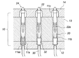
図1は、この発明のプリント配線基板の検査治具の最初の実施例で、検査治具の要部の構成を示した断面図である。図に示すように、この検査治具は、コイルバネ20上にプランジャー22を載置したバネプローブ24を用い、矩形盤状の治具ベース10からプランジャー22の頭部を所定レイアウトで突設して検査ヘッドを形成している。治具ベース10の底面からはリード線30が導出され、測定器側コネクタを接続するコネクタに配線される。
Embodiments of the present invention will be specifically described below with reference to the drawings.
FIG. 1 is a cross-sectional view showing a configuration of a main part of an inspection jig in the first embodiment of the inspection jig for a printed wiring board according to the present invention. As shown in the figure, this inspection jig uses a
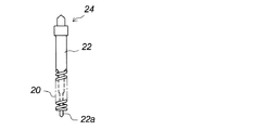
プランジャー22はコイルバネ20の外径と略同一径に形成され、その下半部は先鋭化して下方へ延びる細径部22aを形成している。図2に示すように、バネプローブ24は、細径部22aをコイルバネ20内に挿入し、プランジャー22の上半部をコイルバネ20上に載置した状態で一体として形成されている。また、リード線30の先端をスリーブ32内に挿入し、スリーブ32の外周面をカシメ加工することで一体に結合されている。各部材は電気的に導通する金属材料で形成され、プランジャー22とリード線30は、コイルバネ20、スリーブ32を介して電気的に導通している。
The
治具ベース10は、3枚のプレート12、13、14を積層して形成され、それぞれに上下に貫通した多数の挿通孔11a、11b、11cが所定レイアウトで配置され、各挿通孔11a、11b、11cの位置を揃えて3枚が重ねられている。最下段のプレート12の挿通孔11aには、上面からザグリ加工することで段差係止部11aaが形成され、スリーブ32を係止して脱落を防止している。中段のプレート13の挿通孔11b内にバネプローブ24が収納され、上段のプレート14は、プランジャー22の脱落を防止する保護プレートである。
The
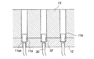
図3、4に、この検査治具の組み付け手順を示す。
最初に、プレート12の上方から、リード線30を結合したスリーブ32を所定の配置に従って挿通孔11a内に挿入する。スリーブ32は段差係止部11aaで係止され、これにプレート13を取り付ける(図3の状態)。
3 and 4 show the procedure for assembling this inspection jig.
First, the
次に、予めコイルバネ20とプランジャー22が一体とされてたバネプローブ24を、プレート13の上方から挿通孔11b内に挿入する。バネプローブ24は、コイルバネ20の底面をスリーブ32に当接して係止され、挿通孔11b内に収納される(図4の状態)。これに上段の保護プレート14を取り付けて検査治具は組み付けられ、プランジャー22の頭部を所定レイアウトで突設した検査ヘッドが形成される。
Next, the
このようにして組み立てた検査治具を用い、上治具と下治具の一対を検査ヘッドを対向させて検査装置に設置し、上治具と下治具の間にプリント配線基板をセットする。そして、検査装置において上方から押圧し、検査ヘッドのプランジャー22の頂端をプリント配線基板の検査接点に当接させ、検査接点間の導通状態を検査する。検査時の押圧でコイルバネ20が収縮してプランジャー22が進退し、押圧の大きさに応じてコイルバネ20が伸縮することで押圧が吸収される。
Using the inspection jig thus assembled, a pair of the upper jig and the lower jig is placed in the inspection apparatus with the inspection head facing each other, and the printed wiring board is set between the upper jig and the lower jig. . Then, pressing is performed from above in the inspection device, and the top end of the
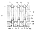
図5は、この発明の検査治具の他の実施例で、検査治具の要部の構成を示した断面図であり、図に示すように、前例よりもさらにバネプローブ24の間隔を狭ピッチとしたものである。前例と同様に、バネプローブ24は、プランジャー22の細径部22aをコイルバネ20内に挿入して一体として形成され、図6に示すように、細径部22aは下方へ延びて下端をコイルバネ20の底面から突設している。この検査治具は前例と同様な手順で組み付けられ、バネプローブ24を挿通孔11b内に収納した状態で、細径部22aの下端をスリーブ32内に挿入している。このように構成することで、検査時の押圧によるコイルバネ20の収縮時に、プランジャー22の進退動作の安定が図られている。
FIG. 5 is a cross-sectional view showing the configuration of the main part of the inspection jig according to another embodiment of the inspection jig of the present invention. As shown in the figure, the interval between the
治具ベース10は、4枚のプレート12a、12b、13、14を積層して形成され、挿通孔11a、11b、11cは、バネプローブ24の細径化に伴ってストレートに開孔することが困難となり、ザグリ加工による段加工で形成されている。スリーブ32は、下段の2枚のプレート12a、12bを重ねて形成される挿通孔11a内に上方から挿入され、最下段のプレート12aの傾斜段差面11abで係止されている。このようにして、検査ヘッドの狭ピッチ化を図った場合、隣接する挿通孔11bが連通し、隣接したコイルバネ20が収縮動作において接触して導通する危険がある。この危険を回避するため、接触した場合にも導通することがないように、コイルバネ20にコーティングが施されている。
The
10 治具ベース
11 挿通孔
12、13、14 プレート
20 コイルバネ
22 プランジャー
22a 細径部
24 バネプローブ
30 リード線
32 スリーブ
DESCRIPTION OF
Claims (4)
治具ベース10を複数枚のプレート12、13、14を積層して形成し、プランジャー22の下半部に下方へ延びる細径部22aを形成し、この細径部22aをコイルバネ20内に挿入して一体としたバネプローブ24を形成し、このバネプローブ24を上方から挿通孔11内に挿入した後、上段の保護プレート14を取り付けて組み付けることを特徴としたプリント配線基板の検査治具。 A printed wiring board in which a plunger 22 is placed on the coil spring 20, the coil spring 20 is accommodated in the insertion hole 11 of the jig base 10, and the head of the plunger 22 is projected in a predetermined layout to form an inspection head. In the inspection jig of
The jig base 10 is formed by laminating a plurality of plates 12, 13, 14, and a small diameter portion 22 a extending downward is formed in the lower half of the plunger 22, and the small diameter portion 22 a is formed in the coil spring 20. An inspection jig for a printed circuit board, in which an integrated spring probe 24 is formed by insertion, the spring probe 24 is inserted into the insertion hole 11 from above, and then an upper protection plate 14 is attached and assembled. .
Priority Applications (1)
| Application Number | Priority Date | Filing Date | Title |
|---|---|---|---|
| JP2004110506A JP2005292060A (en) | 2004-04-02 | 2004-04-02 | Inspection jig for printed circuit board |
Applications Claiming Priority (1)
| Application Number | Priority Date | Filing Date | Title |
|---|---|---|---|
| JP2004110506A JP2005292060A (en) | 2004-04-02 | 2004-04-02 | Inspection jig for printed circuit board |
Publications (1)
| Publication Number | Publication Date |
|---|---|
| JP2005292060A true JP2005292060A (en) | 2005-10-20 |
Family
ID=35325137
Family Applications (1)
| Application Number | Title | Priority Date | Filing Date |
|---|---|---|---|
| JP2004110506A Pending JP2005292060A (en) | 2004-04-02 | 2004-04-02 | Inspection jig for printed circuit board |
Country Status (1)
| Country | Link |
|---|---|
| JP (1) | JP2005292060A (en) |
Cited By (3)
| Publication number | Priority date | Publication date | Assignee | Title |
|---|---|---|---|---|
| WO2008084627A1 (en) * | 2006-12-19 | 2008-07-17 | Nhk Spring Co., Ltd. | Conductive contact unit |
| WO2009102030A1 (en) * | 2008-02-14 | 2009-08-20 | Nhk Spring Co., Ltd. | Probe unit |
| JP2010078432A (en) * | 2008-09-25 | 2010-04-08 | Nidec-Read Corp | Substrate inspection jig and contactor |
-
2004
- 2004-04-02 JP JP2004110506A patent/JP2005292060A/en active Pending
Cited By (4)
| Publication number | Priority date | Publication date | Assignee | Title |
|---|---|---|---|---|
| WO2008084627A1 (en) * | 2006-12-19 | 2008-07-17 | Nhk Spring Co., Ltd. | Conductive contact unit |
| JP5154450B2 (en) * | 2006-12-19 | 2013-02-27 | 日本発條株式会社 | Conductive contact unit |
| WO2009102030A1 (en) * | 2008-02-14 | 2009-08-20 | Nhk Spring Co., Ltd. | Probe unit |
| JP2010078432A (en) * | 2008-09-25 | 2010-04-08 | Nidec-Read Corp | Substrate inspection jig and contactor |
Similar Documents
| Publication | Publication Date | Title |
|---|---|---|
| US8832933B2 (en) | Method of fabricating a semiconductor test probe head | |
| US6469531B1 (en) | Loaded-board, guided-probe test fixture | |
| JP4861860B2 (en) | Printed circuit board inspection jig and printed circuit board inspection apparatus | |
| KR100415245B1 (en) | Probe Card, Probe substrate and Space Transformer using thereto, and Manufacturing Methods thereof | |
| EP3615949B1 (en) | Probe card for a testing apparatus of electronic devices | |
| US10649005B2 (en) | Contact terminal, inspection jig, and inspection device | |
| CN102859370B (en) | Inspection contact element and inspection jig | |
| CN110678759B (en) | Electrical connection device | |
| JP2008145238A (en) | Electrical connector and electrical connection device using the same | |
| JPWO2017212814A1 (en) | Inspection jig and inspection device | |
| KR20210111774A (en) | Contact terminals, inspection jigs and inspection devices | |
| JPWO2004072661A1 (en) | Electrical connection device | |
| JP6283929B2 (en) | Inspection jig and method for manufacturing inspection jig | |
| JP2001153909A (en) | Board inspecting device, board manufacturing method, and board with bump | |
| JP2008216060A (en) | Electrical connection device | |
| JP2008532042A (en) | Probe card having a multilayer substrate | |
| JP2007017234A (en) | Socket for inspection device | |
| JP2018159690A (en) | Electrical connection device | |
| KR101369406B1 (en) | Probe structure and electric tester having a probe structure | |
| JP2020165775A (en) | Probe card | |
| JP5397619B2 (en) | Inspection jig for board inspection | |
| JP2004235591A (en) | Electrical connection device | |
| JP2004138576A (en) | Electrical connection device | |
| JP6665979B2 (en) | Electrical contact | |
| TWI745750B (en) | Electrical connection piece and electrical connection device |
Legal Events
| Date | Code | Title | Description |
|---|---|---|---|
| A621 | Written request for application examination |
Free format text: JAPANESE INTERMEDIATE CODE: A621 Effective date: 20070323 |
|
| A977 | Report on retrieval |
Free format text: JAPANESE INTERMEDIATE CODE: A971007 Effective date: 20090619 |
|
| A131 | Notification of reasons for refusal |
Free format text: JAPANESE INTERMEDIATE CODE: A131 Effective date: 20090630 |
|
| A02 | Decision of refusal |
Free format text: JAPANESE INTERMEDIATE CODE: A02 Effective date: 20091110 |