JP2005291980A - Optical encoder - Google Patents
Optical encoder Download PDFInfo
- Publication number
- JP2005291980A JP2005291980A JP2004108687A JP2004108687A JP2005291980A JP 2005291980 A JP2005291980 A JP 2005291980A JP 2004108687 A JP2004108687 A JP 2004108687A JP 2004108687 A JP2004108687 A JP 2004108687A JP 2005291980 A JP2005291980 A JP 2005291980A
- Authority
- JP
- Japan
- Prior art keywords
- light
- main scale
- signal
- slit
- scale
- Prior art date
- Legal status (The legal status is an assumption and is not a legal conclusion. Google has not performed a legal analysis and makes no representation as to the accuracy of the status listed.)
- Granted
Links
Images


Landscapes
- Optical Transform (AREA)
Abstract
【課題】スケール又はその付帯部材に不連続部分を設けて絶対位置を検出し得る光学式エンコーダを得る。
【解決手段】メインスケール13上に等間隔にスリットSが配列され、スリットS15のみは原点検出のための光線不透過領域とされている。一方、インデックススケール14には3個の矩形状の開口部を1組とした4組の窓W1〜W4が形成され、窓W1〜W4はスリットSのピッチをpとした場合に(1/4)pだけ位相をずらせて配置されている。欠落スリットS15の部分がインデックススケール14と重なると、欠落スリットS15からの光量がフォトダイオードに届かないため、窓W1では3つの開口部のうちの2個分の光しか透過せず、スリット1本分が欠落となることに相当する光量1/3だけ減少し、その値は正規の値の2/3になる。全てのフォトダイオードの出力を足すと、欠落スリットS15による原点信号が得られる。
【選択図】図10An optical encoder capable of detecting an absolute position by providing a discontinuous portion on a scale or its accessory member.
Slits S are arranged at equal intervals on a main scale 13, and only the slit S15 is a light-opaque region for detecting the origin. On the other hand, the index scale 14 is formed with four sets of windows W1 to W4 each including three rectangular openings, and the windows W1 to W4 are (1/4) when the pitch of the slits S is p. ) The phase is shifted by p. When the portion of the missing slit S15 overlaps the index scale 14, the light quantity from the missing slit S15 does not reach the photodiode, so that only two of the three openings are transmitted through the window W1, and one slit is provided. The amount of light is reduced by 1/3 corresponding to the missing portion, and the value becomes 2/3 of the normal value. When the outputs of all the photodiodes are added, the origin signal by the missing slit S15 is obtained.
[Selection] Figure 10
Description
本発明は、変位測定や角度測定に用いられ絶対位置検出を可能とする光学式エンコーダに関するものである。 The present invention relates to an optical encoder that is used for displacement measurement and angle measurement and enables absolute position detection.
光学式エンコーダは基本的に、第1の光学格子が形成されたメインスケールと、これに対向して配置され第2の光学格子が形成されたインデックススケールと、メインスケールに光を照射する光源と、メインスケールの第1の光学格子を透過又は反射し、更にインデックススケールの第2の光学格子から戻ってくる光を受光する受光素子とを備えた構成とされている。 The optical encoder basically includes a main scale on which a first optical grating is formed, an index scale that is disposed opposite to the main scale and on which a second optical grating is formed, and a light source that irradiates the main scale with light. The light receiving element transmits or reflects the first optical grating of the main scale and receives light returning from the second optical grating of the index scale.
この種の光学式エンコーダにおいて、インデックススケールを兼ねて受光素子アレイを用いる方式は、既に例えば特許文献1において提案されている。また、本出願人も同様の構成の特許文献2の光学式エンコーダを出願している。
In this type of optical encoder, a method of using a light receiving element array also serving as an index scale has already been proposed in
このエンコーダはインクリメンタル型と云われ、スケールの移動に対しパルスの増減によりその移動量を検出することが可能である。インクリメンタル型の問題点として、絶対位置が不明なため、絶対位置を検出するセンサが別途に必要になるという問題がある。 This encoder is referred to as an incremental type, and it is possible to detect the movement amount by increasing or decreasing the pulse with respect to the movement of the scale. A problem of the incremental type is that the absolute position is unknown, and therefore a separate sensor for detecting the absolute position is required.
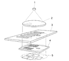
図40はこれらのインクリメンタル式のエンコーダにおける絶対位置を検出する光学式エンコーダの一例を示す斜視図である。LED等の光源1と平行光束に変換するためのコリメータレンズ2、メインスケール3、インデックススケール4、及び複数の受光素子を有する受光部5から成る透過型の光学式エンコーダとして構成されている。
FIG. 40 is a perspective view showing an example of an optical encoder that detects an absolute position in these incremental encoders. It is configured as a transmissive optical encoder including a
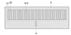
図41はメインスケール3の平面図であり、複数のスリットがS1、S2、・・・、S15、・・・として等間隔に配列され、スリットHが原点信号を発生する目的で標識開口部として設けられている。
41 is a plan view of the
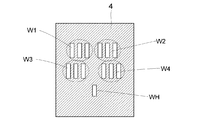
図42はインデックススケール4の平面図を示し、インクリメンタルA、B相信号発生のために設けられた開口パターンを示し、それぞれ3個ずつのスリット状の開口部を有する窓W1、W2、W3、W4は、空間的に90度位相をずらして配置されている。また、窓WHはメインスケール3の原点標識開口部Hに対応している。
FIG. 42 is a plan view of the
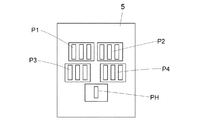
図43は受光部5を示し、フォトダイオードP1、P2、P3、P4はそれぞれ窓W1、W2、W3、W4のスリットを透過してきた光を受光するために設けられている。また、フォトダイオードPHはメインスケール3の原点標識開口部Hに対応し、メインスケール3とインデックススケール4の双方の開口位置が合致したときに光源1からの光が透過し受光部5で受光される。
FIG. 43 shows the
図44は状態a、b、c、dにおいて、インデックススケール4に対してメインスケール3が相対的に1/4ピッチずつずれながら移動してゆく状態を表している。インデックススケール4の開口部とメインスケール3のスリットSの重なりが状態a〜dで徐々に変化し、その変化の結果を受光部5で検出している。図45は図44に示す状態a、b、c、dでのフォトダイオードP1〜P4、PHの出力を示している。
FIG. 44 shows a state in which the
しかし、上述のような従来構成では、原点標識開口部Hの検出のために特別に受光素子が必要で、そのために素子が大型化する。また、この原点検出方法では原点信号発生のための受光素子を設ける必要があり、また光源1の光軸を回転軸としたメインスケール3のアジマスずれにより、インクリメンタル相との位相関係が崩れてしまう問題もある。
However, in the conventional configuration as described above, a light receiving element is specially required for detecting the origin marker opening H, which increases the size of the element. Further, in this origin detection method, it is necessary to provide a light receiving element for generating an origin signal, and the phase relationship with the incremental phase is lost due to the azimuth shift of the
本発明の目的は、上述の問題点を解消し、メインスケール又はその付帯部材に不連続部分を設けてメインスケールの絶対位置をも検出し得る光学式エンコーダを提供することにある。 An object of the present invention is to provide an optical encoder that solves the above-described problems and can detect the absolute position of the main scale by providing a discontinuous portion on the main scale or its accessory member.
上記目的を達成するための本発明に係る光学式エンコーダは、光透過部又は光反射部を連続して配列したメインスケールと、該メインスケールに対して相対移動可能に設けると共に前記光透過部又は光反射部のピッチに関係付けして配設した複数のフォトダイオードを有する受光部と、前記メインスケールを介して前記受光部に光を照射する発光部とを有する光学式エンコーダにおいて、前記メインスケール又は前記メインスケールと共に移動する付帯部材に前記相対移動方向に沿って光学的に不連続部分を設けたことを特徴とする。 In order to achieve the above object, an optical encoder according to the present invention is provided with a main scale in which a light transmitting portion or a light reflecting portion is continuously arranged, and provided relative to the main scale so as to be movable relative to the main scale. In the optical encoder having a light receiving portion having a plurality of photodiodes arranged in relation to the pitch of the light reflecting portion, and a light emitting portion for irradiating light to the light receiving portion through the main scale, the main scale Or the incidental member which moves with the said main scale provided the optically discontinuous part along the said relative movement direction, It is characterized by the above-mentioned.
本発明に係る光学式エンコーダによれば、メインスケール又はその付帯部材に不連続部分を設けたので、安価なコストで絶対位置の検出が可能となる。また、原点検出受光素子が不要となり、極めて小型のエンコーダデバイスが得られる。 According to the optical encoder of the present invention, since the discontinuous portion is provided in the main scale or its accompanying member, the absolute position can be detected at a low cost. In addition, the origin detection light receiving element is unnecessary, and an extremely small encoder device can be obtained.
本発明を図1〜図39に図示の実施例に基づいて詳細に説明する。 The present invention will be described in detail based on the embodiment shown in FIGS.
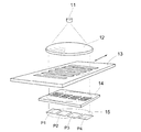
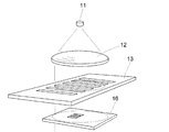
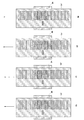
図1は光学式エンコーダの実施例1の斜視図であり、光源11の下方に、コリメータレンズ12、メインスケール13、インデックススケール14、複数のフォトダイオードPを並列した受光部15が順次に配列されている。そして、メインスケール13が他の光学部材に対して矢印方向に相対的に移動可能とされている。
FIG. 1 is a perspective view of an optical encoder according to a first embodiment. A
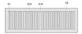
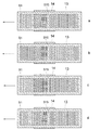
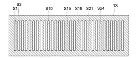
図2はメインスケール13の平面図を示し、メインスケール13上に等間隔に矩形状のスリットS1、・・・・、S10、・・が配列されている。ただし、スリットS15のみは光線不透過領域とされ、原点検出のための特異点とされている。
FIG. 2 is a plan view of the
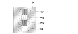
図3はインデックススケール14の平面図を示し、このインデックススケール14にはメインスケール13のスリットSの長さよりも短い長さの3個の矩形状の開口部を1組とした4組の窓W1、W2、W3、W4が形成されている。各開口部はメインスケール13のスリットSと同方向に配列されており、窓W1、W2、W3、W4はメインスケール13のスリットSのピッチをpとした場合に、(1/4)pだけ位相を順次にずらせて開口部の長手方向に沿って配置されている。
FIG. 3 is a plan view of the
この配置により、メインスケール13の変位に応じて90度ずつ位相がずれた信号を発生させることが可能となる。そして、受光部15の4個のフォトダイオードP1〜P4の配列方向は、メインスケール13のスリットS及びインデックススケール14の開口部の長手方向とされている。
With this arrangement, it is possible to generate a signal whose phase is shifted by 90 degrees in accordance with the displacement of the
光源11からの発散光束は、コリメータレンズ12によって平行光束に変換され、メインスケール13を照射する。図4はメインスケール13とインデックススケール14の重なり具合を光源11側から見た平面図である。メインスケール13のスリットSを透過した光束はインデックススケール14に到達し、一部の光束はインデックススケール14の窓W1、W2、W3、W4を透過しそれぞれ受光部15のフォトダイオードP1、P2、P3、P4に入射する。インデックススケール14を通過する光量は、メインスケール13の変位に応じて変化する。
The divergent light beam from the
図5は欠落スリットS15を設けたメインスケール13がインデックススケール14と相対的に変位してゆく状態a〜dを示している。
FIG. 5 shows states a to d in which the
図6はメインスケール13のスリットSを透過した光束によって、インデックススケール14上に形成される光強度分布図である。欠落スリットS15の部分と透過した光束においては光強度分布周期が崩れている。
FIG. 6 is a light intensity distribution diagram formed on the
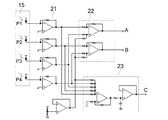
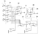
図7は処理回路の構成図を示し、受光部15のフォトダイオードP1〜P4から得られた受光量に見合う電流は、電流電圧回路21において電圧に変換され、変換信号を差動増幅器22に差動入力し、エンコーダ信号A、Bが得られる。また、フォトダイオードP1〜P4の和信号Cが、和算回路23から出力される。
FIG. 7 shows a configuration diagram of the processing circuit. A current corresponding to the amount of light received from the photodiodes P1 to P4 of the
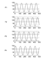
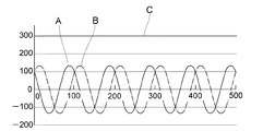
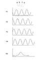
図8は電流電圧回路21の4つの出力信号を示し、インデックススケール14の窓Wの配置により、出力信号は窓W1、W2、W3、W4に対応したフォトダイオードP1、P2、P3、P4の出力位相差の関係を示している。差動増幅器22の出力(P1−P3)、(P2−P4)の結果、図9に示すように波形の90度位相差の信号A、Bが得られる。また、和信号Cはメインスケール13の移動に依存せずに一定した値を示している。
FIG. 8 shows four output signals of the current-
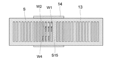
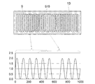
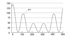
図10はメインスケール13の欠落スリットS15の部分がインデックススケール14と重なった場合のフォトダイオードP1の出力を表し、特に図10では窓W1の部分に注目してその出力の関係を示している。本来、スリットSとして存在しているはずの欠落スリットS15からの光量が、フォトダイオードP1に届かないため、窓W1では3つの開口部のうちの2個分の光しか透過せず、信号の平均電圧レベルはスリット1本分が欠落となることに相当する光量1/3だけ減少し、信号振幅及びDCレベルが低い値になり、その値は正規の値の2/3になる。
FIG. 10 shows the output of the photodiode P1 when the missing slit S15 portion of the
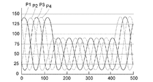
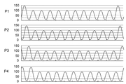
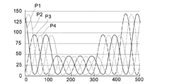
図11はスリットS15がインデックススケール14を通過するときの4個のフォトダイオードP1〜P4の出力信号の位相関係を示している。欠落スリットS15がそれぞれの窓W1〜W4にかかるタイミングが90度の位相差でずれるために、フォトダイオードP1〜P4からはこのような出力波形が得られる。
FIG. 11 shows the phase relationship of the output signals of the four photodiodes P1 to P4 when the slit S15 passes through the
図12はフォトダイオードP1〜P4の4個の信号を全て重ねて表した波形図であり、図13はそのときの差動増幅器22の出力A、Bと和算回路23の出力である和信号Cの変化の様子を表している。
FIG. 12 is a waveform diagram in which all four signals of the photodiodes P1 to P4 are superimposed, and FIG. 13 is a sum signal that is the outputs A and B of the
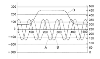
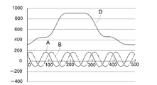
図13に示すように、欠落スリットS15の影響を受けて、受光光量の和信号Cは出力波形周期にして約3周期分、インデックススケール14の開口部の本数分に渡って約2/3に低下し、同時に差動増幅器22の出力信号A、Bの振幅も減少することになる。この和信号Cの変化点は、原点信号として用いることが可能である。
As shown in FIG. 13, under the influence of the missing slit S15, the sum signal C of the amount of received light is about 3/3 of the output waveform period and about 2/3 over the number of openings of the
しかし、更に改善された方法として、図14の信号処理回路に示すような変形例とすれば、差動増幅器22の出力信号A、Bの振幅の減少を回避しながら、上記の変化点を検出することができる。
However, as a further improved method, if the modified example shown in the signal processing circuit of FIG. 14 is used, the above change point is detected while avoiding the decrease in the amplitude of the output signals A and B of the
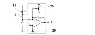
即ち、和算回路23による出力をフィードバック回路24で基準電圧と比較して、光源11の発光量が所定の光量レベルになるようにフィードバックする。光源11を流れる電流値を、オフセット除去回路25が設けられた電流検出回路26により、電圧信号Dとして検出する。なお、電流検出回路26はメインスケール13の欠落スリットS15が通過する電流変化を大きく捉えるために、光量のバイアス分を除去して変化部分を拡大するためにゲインを上げる構成とされている。
That is, the output from the summing
この図14の回路構成では、欠落スリットS15がフォトダイオードP1〜P4を通過したときには、受光部15で得られる光量が少なくなるために、フィードバック回路24により光源11を流れる電流を大きくして、受光部15での光量を一定にするように動作する。このような回路構成によって、欠落スリットS15が存在しても信号振幅が変わらない安定したエンコーダ信号A、Bが得られることになる。
In the circuit configuration of FIG. 14, when the missing slit S15 passes through the photodiodes P1 to P4, the amount of light obtained by the
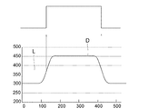
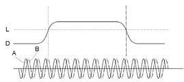
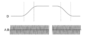
図15は受光部15がスリット8波分の幅を持っている場合に、メインスケール13の欠落スリットS15が通過したときの電流検出回路26で得られる信号Dと、差動増幅器22から得られるエンコーダ信号A、Bを示している。信号A、Bの振幅は殆ど変化なく、信号Dはメインスケール13による欠落スリットS15の特異点つまり原点位置で変化している。従って、例えば図16に示すようにコンパレータにより適宜に信号Dを基準電圧Lと比較することで、矩形波信号を得て原点信号として用いることが可能となる。
FIG. 15 shows the signal D obtained by the
図17は実施例2のメインスケール13の平面図である。実施例1に対して、本実施例2では欠落スリットSは1個所ではなく、スリットS15以外にスリットS18、S21、S24と、2個おきに欠落スリットSが設けられている。
FIG. 17 is a plan view of the
フォトダイオードP1〜P4から図18に示すような信号が得られ、原点信号ではなく或る広い領域を定義する場合に有効である。この場合には、出力信号周期にして約10周期分のゾーン定義が可能となる。 Signals as shown in FIG. 18 are obtained from the photodiodes P1 to P4, which is effective when defining a wide area rather than the origin signal. In this case, it is possible to define a zone for about 10 cycles as an output signal cycle.
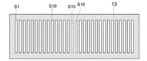
図19は実施例3によるメインスケール13による欠落点の設け方として、連続したスリットS15、S16が欠落スリットとされている。インデックススケール14の窓W1、W2、W3、W4は図2で示したように3個の開口部を組にして1つの窓Wと対応している。従って、欠落スリットS15、S16が連続して欠落しても、残りの1個の窓Wで光を受光することが可能なため、インクリメンタル相の信号A、Bは歯抜けになることはない。
In FIG. 19, continuous slits S <b> 15 and S <b> 16 are defined as missing slits as a method of providing missing points by the
図20、図21はそれぞれ1個のフォトダイオードPの出力、4個のフォトダイオードP1〜P4の出力を示し、3個の窓Wのうちの2個分を覆うような状態では出力は正規の値の1/3まで落ち込むが、図14の信号処理回路を適用することで、図22に示すように信号A、Bの信号振幅を安定に保ちながら、光源11の電流の変化点を捉え、電流検出回路26の出力信号Dを原点信号として使用できる。
FIGS. 20 and 21 respectively show the output of one photodiode P and the outputs of four photodiodes P1 to P4. In the state where two of the three windows W are covered, the output is normal. Although it drops to 1/3 of the value, by applying the signal processing circuit of FIG. 14, the change point of the current of the
実施例1ではインデックススケール14と受光部15を別個にして用いたが、実施例4では図23に示すようにインデックススケール14と受光部15が一体的に集積されたフォトダイオードアレイ16が用いられている。
In the first embodiment, the
図24はフォトダイオードアレイ16の配列を示し、フォトダイオードP1、P2、P3、P4が受光エレメントとして0゜、90゜、180゜、270゜の関係になるように繰り返して規則正しく並べられ、実施例1と同様の受光信号が得られ、このフォトダイオードアレイ16を用いることで更に高精度な原点検知が可能となる。実施例1では、光源11からの照射光量を効率的に受光することが困難であるが、このフォトダイオードアレイ16では、光源光軸のほぼ中央に受光部15を配置することができる。
FIG. 24 shows the arrangement of the
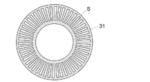
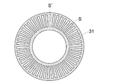
図25は実施例5による透過型ロータリエンコーダ用のメインスケール31を示している。このメインスケール31は放射方向に多数個のスリットSが設けられているが、図26に示すように1つの欠落スリットS’を設けて原点信号としている。基本的な動作は実施例1と同様なので説明は省略する。
FIG. 25 shows a
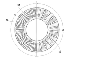
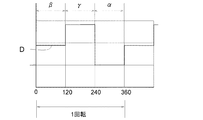
図27は実施例2、実施例3の欠落スリットの配列をメインスケール31に適用したものであり、180゜ずつの2つの領域α、βに分けられ、領域βにおいては領域αに対してスリットSが1つおきに間引かれている。
FIG. 27 shows an example in which the arrangement of the missing slits in the second and third embodiments is applied to the
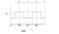
図28は電流検出回路26からの信号Dを基とする矩形波の波形を示し、領域αとβとで信号Dのレベルが明瞭に識別でき、領域α、βを区別することができる。
FIG. 28 shows a rectangular wave waveform based on the signal D from the
ロータリ式エンコーダでは、例えばモータ駆動制御用の出力信号としてUVW信号(コミュテーション信号)を生成する必要があるが、その場合にも図29に示すようにスリットSの密度を領域α、β、γにおいて変えることにより、3種類の異なるゾーン定義が可能となり、UVW信号の置き換えが可能である。そして、この場合には図30に示すような信号Dが得られる。 In the rotary encoder, for example, it is necessary to generate a UVW signal (commutation signal) as an output signal for motor drive control. In this case as well, the density of the slits S is set to regions α, β, γ as shown in FIG. By changing in, three different zones can be defined, and the UVW signal can be replaced. In this case, a signal D as shown in FIG. 30 is obtained.
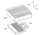
図31は実施例6を示し、移動体であるメインスケール41の形状を、反射型のマイクロルーフミラーアレイとした直線移動式エンコーダの光学系の構成図であり、このような構成を採用することにより、光の利用効率を向上させることができる。このマイクロルーフミラーアレイを用いた構成については、特許文献4に開示されている。なお、受光部42に対し相対的にかつ直線状にX方向に移動するメインスケール41の反射部には、反射部のX方向への連続性を損う非反射部による欠落部41aが部分的に設けられている。
FIG. 31 shows a sixth embodiment, and is a configuration diagram of an optical system of a linearly movable encoder in which the shape of the
この光学式エンコーダは、メインスケール41、複数のフォトダイオードPを並列した受光部42、光源43から成り、光源43で発光した光が、細かい間隔の反射部と非反射部を持つメインスケール41で反射して、受光部42上に明暗の分布を与える。
This optical encoder is composed of a
この構成は、特にメインスケール41がマイクロルーフミラーアレイを用いた構成でなく、単に反射部と非反射部を持つ構成であれば、信号レベルは異なるものの、同様な光の明暗の分布が受光部42上に形成され、エンコーダ信号A、Bを得ることが可能である。
In this configuration, if the
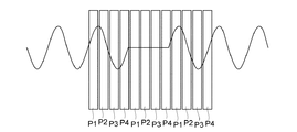
図32は複数のフォトダイオードPを配列した受光部42の構成と入力光の明暗パターンの説明図であり、フォトダイオードP1、P2、P3、P4はそれぞれ0゜、90゜、180゜、270゜の関係になるように繰り返して配置されている。入力光の明暗パターンが欠落部41aによって部分的に欠落しても、他のフォトダイオードPの存在のために、ほぼフォトダイオードPの残っている割合での信号振幅が得られる。
FIG. 32 is an explanatory diagram of the configuration of the
この実施例6の構成では図14の回路構成が使用でき、図33はフォトダイオードPがスリット8波分の幅を持っている場合のときの信号出力である。この図33から分かるようにメインスケール41の欠落部41aが1つの場合に、最初に受光部42に欠落部41aがかかったときに光量が減少するので、フィードバック回路24では電流を増加する。従って、電流検出回路26の信号Dは約1/8の割合で増加する。そして、その状態が受光部42に欠落部41aがかかっている間続き、受光部42から外れると元の信号レベルに低下する。
In the configuration of the sixth embodiment, the circuit configuration of FIG. 14 can be used, and FIG. 33 shows the signal output when the photodiode P has a width corresponding to 8 waves of the slit. As can be seen from FIG. 33, when the number of
このような構成にすることで、エンコーダ信号A、Bに変化を与えることなく、メインスケール41の欠落部41aが通過したことを信号Dにより検出することができる。
With such a configuration, it is possible to detect from the signal D that the missing
ここで、メインスケール41の欠落部41aは1つのときの実施例を示したが、欠落部41aが連続した2つであれば電流変化も2倍になり、電流検出回路26の信号Dのレベルの変化も大きくなる。これを利用することにより、信号Dのレベルにより何個の欠落部41aが受光部42上を通過しているかが分かるので、メインスケール41に特殊なパターンを構成することにより絶対位置の検出にも利用できる。
Here, the embodiment in which the number of
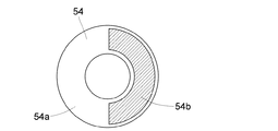
図34は実施例7の回転型の光学式エンコーダにおける透過型のメインスケール51等の光学的な構成図を示している。メインスケール51には不連続部分を設けずに、メインスケール51の受光部52、光源53とは反対側に、メインスケール51を透過した光を反射して、受光部52に戻す効果を有する反射板54が設けられている。この反射板54は保持部材55に張り付けられ、メインスケール51と共に共通の回転軸56により回転するようにされている。
FIG. 34 shows an optical configuration diagram of the transmissive
図35は反射板54の反射部54aと非反射部54bのパターンを示し、反射部54aと非反射部54bが丁度半分半分の半月状の形状とされ、非反射部54bが回転方向に対する不連続部分となっている。
FIG. 35 shows a pattern of the reflecting
光源53から出射した光は光路L1を経てメインスケール51に至り、メインスケール51で反射して受光部52に戻って位置パルスのエンコーダ信号A、Bを発生させる。また、光源53で発光した光の一部はメインスケール51を光路L2のように通過し、反射板54の反射部54aで反射してメインスケール51を経て受光部52に戻る。
The light emitted from the
この光路L2による光はエンコーダ信号A、Bとは異なり、絶対位置を得るための信号Dを発生するためのものであり、メインスケール51の反射パターンとは関係のないDC光である。従って、受光部52はメインスケール51の裏側に反射部54aがあるときは、DC光が入ってきたかのような動作となり、光源53の光量を絞る方向に動作する。
Unlike the encoder signals A and B, the light on the optical path L2 is for generating a signal D for obtaining an absolute position, and is DC light that is not related to the reflection pattern of the
図36はこの実施例7の構成において、図14に示す回路からの信号A、B、Dを示し、反射板54の反射部54aが受光部52上に至ると、反射してきた光の影響で、光源52の電流を減らす挙動となる。従って、この変化により実施例1と同様に、絶対位置に対応した位置情報が得られる。
FIG. 36 shows signals A, B and D from the circuit shown in FIG. 14 in the configuration of the seventh embodiment. When the reflecting
本実施例7では、メインスケール51に加工を加えることなく、つまりメインスケール51には不連続部分を設けることなく、非反射部54bを有する反射板54をメインスケール51の裏側に配置するだけで、絶対位置情報が得られる利点がある。また、反射板54の反射部54aと非反射部54bのパターンを変えて信号Dのハイレベルとローレベルの区間を変更したり、反射板54の反射率を変えることにより、ハイレベルとローレベルの差を変化させることも可能である。
In the seventh embodiment, the
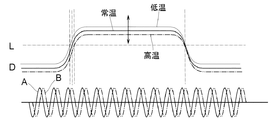
図37は温度環境に対応していないときの電流検出回路26の信号Dを示し、温度環境が変わることによって、光源11を流れる電流のオフセットが大きく上下する。光源11で同じ発光量を得るためには、電流は高温では少なく、低温では増やす必要がある。また、受光部15の温度特性としては、高温で検出電圧が上がり、低温で検出電圧が下がる傾向にある。
FIG. 37 shows the signal D of the
その他にも、温度によって特性変化する部材が存在するが、図37はこれらの各部材の温度特性を合成した特性を基にしたエンコーダ信号A、B及び電流検出回路26の信号Dの波形図である。この温度特性は高温で同じ光量を得るためには電流値が下がり、低温では電流値が上がる傾向となっている。このとき、信号Dを基準電圧Lと比較する場合に、信号Dの立上部は基準電圧Lと交叉する位置は温度によって大きくずれて、絶対位置の検出に誤差が介入されるという問題がある。
There are other members whose characteristics change depending on the temperature. FIG. 37 is a waveform diagram of the encoder signals A and B and the signal D of the
図38はこの温度特性を改善するための回路構成図を示し、基本構成は図14と同様であるが、本実施例8では光源11に直列に接続されている抵抗Rが、正の温度特性を持つ感温抵抗とされている。これにより、高温時に電流が減少しても抵抗Rの値は増えるため、電流検出回路26からの信号Dが上昇し、それぞれが打ち消し合うことになる。
FIG. 38 shows a circuit configuration diagram for improving this temperature characteristic. The basic configuration is the same as that of FIG. 14, but in the eighth embodiment, the resistor R connected in series with the
従って、抵抗Rの温度係数と受光部15の電流変化の温度特性を組み合わせることにより、温度変化があっても図39に示すように信号Dが大きく変わることがなく、基準電圧Lと交叉する位置である原点検出を正確に求めることが可能となる。
Therefore, by combining the temperature coefficient of the resistor R and the temperature characteristic of the current change in the
本実施例8では、抵抗Rを感温抵抗にする手段を用いたが、オフセット除去回路25の部分に温度補償回路を設けるようにすることも可能である。
In the eighth embodiment, the means for changing the resistance R to the temperature-sensitive resistance is used. However, a temperature compensation circuit may be provided in the portion of the offset
11、43、53 光源
12 コリメータレンズ
13、31、41、51 メインスケール
14 インデックススケール
15、42、52 受光部
16 フォトダイオードアレイ
21 電流電圧回路
22 差動増幅器
23 和算回路
24 フィードバック回路
25 オフセット除去回路
26 電流検出回路
54 反射板
55 保持部材
56 回転軸
P フォトダイオード
S スリット
W 窓
DESCRIPTION OF
Claims (5)
Priority Applications (8)
| Application Number | Priority Date | Filing Date | Title |
|---|---|---|---|
| JP2004108687A JP4474188B2 (en) | 2004-04-01 | 2004-04-01 | Optical encoder |
| EP05004593A EP1577645B1 (en) | 2004-03-17 | 2005-03-02 | Optical encoder |
| DE602005002287T DE602005002287T2 (en) | 2004-03-17 | 2005-03-02 | Optical encoder |
| US11/075,959 US7132647B2 (en) | 2004-03-17 | 2005-03-09 | Optical encoder |
| CNB2005100554535A CN100389305C (en) | 2004-03-17 | 2005-03-17 | Optical encoder |
| KR1020050022194A KR100753062B1 (en) | 2004-03-17 | 2005-03-17 | Optical encoder |
| US11/535,298 US7326919B2 (en) | 2004-03-17 | 2006-09-26 | Optical encoder |
| KR1020070029126A KR100738495B1 (en) | 2004-03-17 | 2007-03-26 | Optical encoder |
Applications Claiming Priority (1)
| Application Number | Priority Date | Filing Date | Title |
|---|---|---|---|
| JP2004108687A JP4474188B2 (en) | 2004-04-01 | 2004-04-01 | Optical encoder |
Publications (3)
| Publication Number | Publication Date |
|---|---|
| JP2005291980A true JP2005291980A (en) | 2005-10-20 |
| JP2005291980A5 JP2005291980A5 (en) | 2007-05-31 |
| JP4474188B2 JP4474188B2 (en) | 2010-06-02 |
Family
ID=35325064
Family Applications (1)
| Application Number | Title | Priority Date | Filing Date |
|---|---|---|---|
| JP2004108687A Expired - Fee Related JP4474188B2 (en) | 2004-03-17 | 2004-04-01 | Optical encoder |
Country Status (1)
| Country | Link |
|---|---|
| JP (1) | JP4474188B2 (en) |
Cited By (5)
| Publication number | Priority date | Publication date | Assignee | Title |
|---|---|---|---|---|
| JP2008028025A (en) * | 2006-07-19 | 2008-02-07 | Canon Inc | Reflective sensor |
| JP2010160147A (en) * | 2008-12-23 | 2010-07-22 | Avago Technologies Ecbu Ip (Singapore) Pte Ltd | Single track optical encoder |
| US8035724B2 (en) | 2006-10-06 | 2011-10-11 | Canon Kabushiki Kaisha | Method and apparatus for controlling lens position |
| JP2012042635A (en) * | 2010-08-18 | 2012-03-01 | Canon Inc | Imaging device, control method for imaging devices and computer program |
| JP2013041000A (en) * | 2011-08-11 | 2013-02-28 | Olympus Imaging Corp | Interchangeable lens |
-
2004
- 2004-04-01 JP JP2004108687A patent/JP4474188B2/en not_active Expired - Fee Related
Cited By (6)
| Publication number | Priority date | Publication date | Assignee | Title |
|---|---|---|---|---|
| JP2008028025A (en) * | 2006-07-19 | 2008-02-07 | Canon Inc | Reflective sensor |
| US8035724B2 (en) | 2006-10-06 | 2011-10-11 | Canon Kabushiki Kaisha | Method and apparatus for controlling lens position |
| EP1909129B1 (en) * | 2006-10-06 | 2017-08-23 | Canon Kabushiki Kaisha | Method and apparatus for controlling lens position |
| JP2010160147A (en) * | 2008-12-23 | 2010-07-22 | Avago Technologies Ecbu Ip (Singapore) Pte Ltd | Single track optical encoder |
| JP2012042635A (en) * | 2010-08-18 | 2012-03-01 | Canon Inc | Imaging device, control method for imaging devices and computer program |
| JP2013041000A (en) * | 2011-08-11 | 2013-02-28 | Olympus Imaging Corp | Interchangeable lens |
Also Published As
| Publication number | Publication date |
|---|---|
| JP4474188B2 (en) | 2010-06-02 |
Similar Documents
| Publication | Publication Date | Title |
|---|---|---|
| KR100738495B1 (en) | Optical encoder | |
| JP5318212B2 (en) | How to index an optical encoder | |
| CN101529211B (en) | Rotary Optical Encoder Using Multiple Sub-Encoders With Common Grazed Substrate | |
| JP4678553B2 (en) | Optical encoder | |
| US7732757B2 (en) | Origin detection method for optical encoder | |
| JP5046523B2 (en) | Position measuring device | |
| JP4498024B2 (en) | Optical encoder | |
| JPH0658779A (en) | Measuring device | |
| US7391011B2 (en) | Optical encoder capable of detecting absolute position | |
| US9116163B2 (en) | Displacement measuring apparatus | |
| JP4474188B2 (en) | Optical encoder | |
| JP3881339B2 (en) | Position measuring device | |
| JPH09113213A (en) | Device for filtering higher-harmonic signal component | |
| JP2009047595A (en) | Absolute position length-measurement type encoder | |
| JP2005265512A (en) | Optical encoder | |
| JP2007078690A (en) | Reflective optical encoder | |
| US7196319B2 (en) | Position-measuring device | |
| JP2012233755A (en) | Optical encoder and absolute position detecting method for the same | |
| JP2004347358A (en) | Displacement measuring apparatus | |
| JP2001174290A (en) | Talbot array type rotary encoder | |
| JPH03267719A (en) | Reference position detector and encoder using the same |
Legal Events
| Date | Code | Title | Description |
|---|---|---|---|
| A521 | Written amendment |
Free format text: JAPANESE INTERMEDIATE CODE: A523 Effective date: 20070330 |
|
| A621 | Written request for application examination |
Free format text: JAPANESE INTERMEDIATE CODE: A621 Effective date: 20070330 |
|
| A977 | Report on retrieval |
Free format text: JAPANESE INTERMEDIATE CODE: A971007 Effective date: 20090716 |
|
| A131 | Notification of reasons for refusal |
Free format text: JAPANESE INTERMEDIATE CODE: A131 Effective date: 20090721 |
|
| A521 | Written amendment |
Free format text: JAPANESE INTERMEDIATE CODE: A523 Effective date: 20090924 |
|
| A131 | Notification of reasons for refusal |
Free format text: JAPANESE INTERMEDIATE CODE: A131 Effective date: 20091020 |
|
| RD01 | Notification of change of attorney |
Free format text: JAPANESE INTERMEDIATE CODE: A7421 Effective date: 20100218 |
|
| TRDD | Decision of grant or rejection written | ||
| A01 | Written decision to grant a patent or to grant a registration (utility model) |
Free format text: JAPANESE INTERMEDIATE CODE: A01 Effective date: 20100302 |
|
| A01 | Written decision to grant a patent or to grant a registration (utility model) |
Free format text: JAPANESE INTERMEDIATE CODE: A01 |
|
| A61 | First payment of annual fees (during grant procedure) |
Free format text: JAPANESE INTERMEDIATE CODE: A61 Effective date: 20100308 |
|
| FPAY | Renewal fee payment (event date is renewal date of database) |
Free format text: PAYMENT UNTIL: 20130312 Year of fee payment: 3 |
|
| R150 | Certificate of patent or registration of utility model |
Free format text: JAPANESE INTERMEDIATE CODE: R150 |
|
| FPAY | Renewal fee payment (event date is renewal date of database) |
Free format text: PAYMENT UNTIL: 20140312 Year of fee payment: 4 |
|
| LAPS | Cancellation because of no payment of annual fees |