JP4498024B2 - Optical encoder - Google Patents
Optical encoder Download PDFInfo
- Publication number
- JP4498024B2 JP4498024B2 JP2004177407A JP2004177407A JP4498024B2 JP 4498024 B2 JP4498024 B2 JP 4498024B2 JP 2004177407 A JP2004177407 A JP 2004177407A JP 2004177407 A JP2004177407 A JP 2004177407A JP 4498024 B2 JP4498024 B2 JP 4498024B2
- Authority
- JP
- Japan
- Prior art keywords
- signal
- amplitude
- scale
- center voltage
- value
- Prior art date
- Legal status (The legal status is an assumption and is not a legal conclusion. Google has not performed a legal analysis and makes no representation as to the accuracy of the status listed.)
- Expired - Fee Related
Links
Images


Classifications
-
- G—PHYSICS
- G01—MEASURING; TESTING
- G01D—MEASURING NOT SPECIALLY ADAPTED FOR A SPECIFIC VARIABLE; ARRANGEMENTS FOR MEASURING TWO OR MORE VARIABLES NOT COVERED IN A SINGLE OTHER SUBCLASS; TARIFF METERING APPARATUS; MEASURING OR TESTING NOT OTHERWISE PROVIDED FOR
- G01D5/00—Mechanical means for transferring the output of a sensing member; Means for converting the output of a sensing member to another variable where the form or nature of the sensing member does not constrain the means for converting; Transducers not specially adapted for a specific variable
- G01D5/26—Mechanical means for transferring the output of a sensing member; Means for converting the output of a sensing member to another variable where the form or nature of the sensing member does not constrain the means for converting; Transducers not specially adapted for a specific variable characterised by optical transfer means, i.e. using infrared, visible, or ultraviolet light
- G01D5/32—Mechanical means for transferring the output of a sensing member; Means for converting the output of a sensing member to another variable where the form or nature of the sensing member does not constrain the means for converting; Transducers not specially adapted for a specific variable characterised by optical transfer means, i.e. using infrared, visible, or ultraviolet light with attenuation or whole or partial obturation of beams of light
- G01D5/34—Mechanical means for transferring the output of a sensing member; Means for converting the output of a sensing member to another variable where the form or nature of the sensing member does not constrain the means for converting; Transducers not specially adapted for a specific variable characterised by optical transfer means, i.e. using infrared, visible, or ultraviolet light with attenuation or whole or partial obturation of beams of light the beams of light being detected by photocells
- G01D5/36—Forming the light into pulses
- G01D5/366—Particular pulse shapes
Landscapes
- Physics & Mathematics (AREA)
- General Physics & Mathematics (AREA)
- Optical Transform (AREA)
Description
本発明は、変位測定や角度測定に用いられる光学式エンコーダに関するものである。 The present invention relates to an optical encoder used for displacement measurement and angle measurement.
光学式エンコーダは基本的に、第1の光学格子が形成されたメインスケールと、これに対向して配置され第2の光学格子が形成されたインデックススケールと、メインスケールに光を照射する光源と、メインスケールの光学格子を透過又は反射し、更にインデックススケールの光学格子を透過した光を受光する受光素子とを備えて構成されている。 The optical encoder basically includes a main scale on which a first optical grating is formed, an index scale that is disposed opposite to the main scale and on which a second optical grating is formed, and a light source that irradiates the main scale with light. And a light receiving element that receives or reflects light transmitted through the optical grating of the main scale and further transmitted through the optical grating of the index scale.
この種の光学式エンコーダにおいて、インデックススケールを兼ねて受光素子アレイを用いる方式は、既に特許文献1に提案されている。また、本発明者もこの構成のエンコーダとして、特許文献2に開示の発明を出願している。
In this type of optical encoder, a method using a light receiving element array also serving as an index scale has already been proposed in
この構成のエンコーダはインクリメンタル型と云われ、スケールの移動に対し、パルスの増減によりその移動量を検出することが可能である。 The encoder having this configuration is called an incremental type, and can detect the movement amount of the scale by moving the scale up or down.
このインクリメンタル型の問題として、回転角度の絶対位置が分からないために、絶対位置を検出するセンサを別途必要とする問題があるが、それを回避する手段として特許文献3が開示されている。
As an incremental type problem, since the absolute position of the rotation angle is not known, there is a problem that a sensor for detecting the absolute position is separately required.
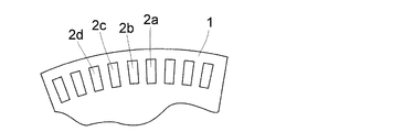
この特許文献3においては、インクリメンタル式の透過型のエンコーダにおける絶対値を検出するために、図13に示すようにスケール1に配列したスリット2の透過率を変化させ、例えばスリット2aの透過率を1とし、並列する順次のスリット2b、2c、2dの透過率を徐々に低下させている。
In
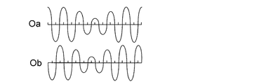
図14はこのスケール1を用いて、センサをスリット2の透過率が変化している部分が通過したときに得られる信号変化を示しており、センサから得られるアナログ2相信号Oa、Obは、スリット2の透過率が徐々に低下することにより振幅が低下するので、この変化を検出することによって絶対位置を検出するようになっている。
FIG. 14 shows the signal change obtained when the portion where the transmittance of the
上述の従来例で示すエンコーダの絶対位置検出手段では、信号振幅を検出する方法として、得られるエンコーダ信号の1周期よりも十分に細かいタイミングでサンプリングし、そこから得られる信号のピークとバレイの電圧を求めなければならず、この処理のために高速なAD変換器など規模の大きな回路が必要となる。また、スケールに透過率の異なる部分を正確に製作する必要があり、実際の振幅変化もかなりのばらつきが発生する問題がある。 In the encoder absolute position detecting means shown in the above-mentioned conventional example, as a method for detecting the signal amplitude, sampling is performed at timing sufficiently finer than one period of the obtained encoder signal, and the peak of the signal obtained and the voltage of the valley are obtained. For this processing, a large-scale circuit such as a high-speed AD converter is required. In addition, it is necessary to accurately manufacture portions having different transmittances on the scale, and there is a problem that a substantial variation occurs in the actual amplitude change.
本発明の目的は、上述の問題点を解消し、簡単な構成で不連続部分が得られるスケール構成とし、環境変化の影響を受けることのない信号や信号処理を用いて、スケールに付した不連続部分の位置を原点として安定して検出することを可能とする光学式エンコーダを提供することにある。 An object of the present invention is to eliminate the above-mentioned problems and to provide a scale configuration that can obtain a discontinuous portion with a simple configuration, and using a signal and signal processing that are not affected by environmental changes, An object of the present invention is to provide an optical encoder that can stably detect the position of a continuous portion as an origin.
上記目的を達成するための本発明に係る光学式エンコーダは、所定の間隔の光学格子が形成され、前記光学格子の一部に光学的な不連続部分が設けられたスケールと、該スケールに対して相対移動可能に設けられ、光源から照射された光束を前記スケールを介して受光する複数の受光素子を1セグメントとし、複数の前記セグメントを有し、複数の前記セグメント間の互いに対応する位置からは同位相の出力が得られるよう前記光学格子のピッチに関係付けして配設した受光素子アレイと、前記受光素子アレイから得られる電気信号に基づいてインクリメンタル信号を得る信号処理回路とを有する光学式エンコーダにおいて、前記信号処理回路は、前記インクリメンタル信号として互いに位相が90°ずれた2つのアナログ信号と、前記2つのアナログ信号と位相が等しく、前記アナログ信号の2値化された信号である2つのデジタル信号とを出力し、少なくとも一方のデジタル信号のパルスエッジのタイミングで得られる前記一方のデジタル信号と位相が90°ずれた前記アナログ信号の値に基づいて、前記位相が90°ずれたアナログ信号の振幅又は中心電圧を求め、前記不連続部材が前記受光素子アレイを通過するときに前記振幅又は前記中心電圧の変化を検出し、該変化が発生したときの位置に基づいて原点を検出することを特徴とする。 In order to achieve the above object, an optical encoder according to the present invention includes a scale in which optical gratings having a predetermined interval are formed, and an optical discontinuity is provided in a part of the optical grating , and the scale. The plurality of light receiving elements that are provided so as to be relatively movable and receive the light beam emitted from the light source through the scale are defined as one segment, have a plurality of the segments, and from a position corresponding to each other between the plurality of segments. Is an optical device having a light receiving element array disposed in relation to the pitch of the optical grating so as to obtain an in-phase output, and a signal processing circuit for obtaining an incremental signal based on an electric signal obtained from the light receiving element array. in formula encoder, the signal processing circuit includes two analog signals phase shifted 90 ° from each other as said incremental signal, the two Two digital signals that are equal in phase to the analog signal and are binarized from the analog signal are output, and the phase of the one digital signal obtained at the timing of the pulse edge of at least one of the digital signals is 90. ° out based on the value of the analog signal, obtains the amplitude or the center voltage of the analog signal which the phases are shifted 90 °, the amplitude or the center voltage when the discontinuity member passes through the light receiving element array detecting a change, and detects the origin based on the position at which said change has occurred.
本発明に係る光学式エンコーダによれば、絶対位置検出を行う際にアナログエンコーダ信号振幅の変化点或いは中心電圧の変化点を検出することにより、スケールの不連続部分の位置を検出することを可能とし、スケールの絶対位置を簡素な電気回路により検出することができる。 According to the optical encoder of the present invention, it is possible to detect the position of the discontinuous portion of the scale by detecting the change point of the analog encoder signal amplitude or the change point of the center voltage when performing absolute position detection. And the absolute position of the scale can be detected by a simple electric circuit.
本発明を図示の実施例に基づいて詳細に説明する。 The present invention will be described in detail based on the embodiments shown in the drawings.
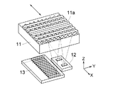
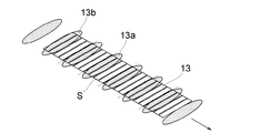
図1は反射型スケールの形状をマイクロルーフミラーアレイとした光学式エンコーダの構成図である。従来では、発光部と受光部とがスケールを挟んで対向して設置された所謂透過型の構成であったが、本実施例1では反射型の構成とされている。また、スケール11の形状をマイクロルーフミラーアレイを用いた構成とすることにより、光の利用効率を向上させている。このマイクロルーフミラーアレイについては、特許文献4に開示されている。
FIG. 1 is a configuration diagram of an optical encoder in which the shape of a reflective scale is a micro roof mirror array. Conventionally, the light-emitting unit and the light-receiving unit have a so-called transmissive configuration in which the scale and the light-receiving unit are opposed to each other, but in the first embodiment, a reflective configuration is used. Moreover, the utilization efficiency of light is improved by making the shape of the
移動体であるスケール11の片側には、発光部12、複数の受光素子を列状に配置した受光部13が固定して配置されている。発光部12で発光した光は、細かい間隔の反射部と非反射部を持つスケール11で反射して図2の受光部13の受光素子の列上に明暗の分布を与える。この構成は特にスケール11がマイクロルーフミラーアレイを用いた構成ではなく、単に反射部と非反射部を持つ構成であれば、信号レベルは異なるものの、同様な光の明暗の分布が受光部13上に形成され、エンコーダ信号を得ることができる。
On one side of the
従来のスケールでは前述したように、不連続部分として透過率が異なる部分を構成していたが、本実施例1では光束が完全に透過しない不連続部分11aがスケール11に設けられている。従来例において透過率が異なる部分を設けていたのは、完全な不完全部分を設けると信号が欠落しエラーとなってしまうため、或る程度の信号振幅が必要であったためである。
In the conventional scale, as described above, the discontinuous portion has a portion having different transmittance. However, in the first embodiment, the
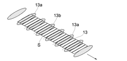
図2に示す受光部13は、4個のフォトダイオードSを1セグメントとし、複数のセグメントを有する構成とされている。13aはスケール11を介して受光部13に戻ってきた光の強度が強い部分である。通常のエンコーダでは、この光強度の強い部分13aがスケール11のピッチと或る関係で分布する。本実施例1の構成では、4つのフォトダイオードSのセグメントと同じ間隔で13aの部分が分布することになる。
The
本実施例1では、スケール11に不連続部分11aを設けているため、13bに示すように光強度の強い部分が抜ける現象が生ずる。しかし、この構成によれば入力光の波がスケール11の不連続部分11aに従って、完全に1つ欠落したとしても、他のフォトダイオードSの存在のために、ほぼフォトダイオードSが残っている割合での信号振幅が得られる。
In the first embodiment, since the
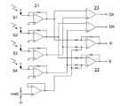
図3は本実施例の回路構成図であり、フォトダイオードS1〜S4の出力はそれぞれ電流電圧変換器21に接続されている。フォトダイオードS1〜S4からはそれぞれ位相が90゜ずれた信号が出力され、フォトダイオードS1とS3、S2とS4からのそれぞれ位相が180°ずれた信号が、2個の差動増幅器22及び2個のコンパレータ23のプラス入力とマイナス入力に入力して2値化され、アナログエンコーダ信号(以下、アナログ信号と云う)A、Bと、デジタルエンコーダ信号(以下、デジタル信号と云う)DA、DBが得られる。
FIG. 3 is a circuit configuration diagram of this embodiment, and the outputs of the photodiodes S1 to S4 are connected to the current-
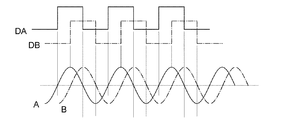
図4は図3の回路構成から得られた信号のタイムチャート図である。デジタル信号DA、DBはアナログ信号A、Bのゼロクロスにおいて生成されており、しかもアナログ信号A、Bは90°位相がずれているため、デジタル信号DBの立上りと立下りはアナログ信号Aの最大と最小の値になる。 FIG. 4 is a time chart diagram of signals obtained from the circuit configuration of FIG. Since the digital signals DA and DB are generated at the zero crossing of the analog signals A and B, and the analog signals A and B are 90 ° out of phase, the rising and falling edges of the digital signal DB are the maximum of the analog signal A. It becomes the minimum value.
従って、デジタル信号DBのパルスエッジのタイミングでアナログ信号Aの信号を取り込めば、アナログ信号Aの最大値と最小値の値が得られる。 Therefore, if the signal of the analog signal A is taken in at the timing of the pulse edge of the digital signal DB, the maximum value and the minimum value of the analog signal A can be obtained.
また、アナログ信号Aの振幅は(アナログ信号Aの最大値−アナログ信号Aの最小値)から求められ、アナログ信号Aの中心電圧は、{(アナログ信号Aの最大値+アナログ信号Aの最小値)/2}から求めることができる。 The amplitude of the analog signal A is obtained from (the maximum value of the analog signal A−the minimum value of the analog signal A), and the center voltage of the analog signal A is {(the maximum value of the analog signal A + the minimum value of the analog signal A). ) / 2}.
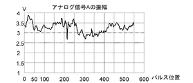
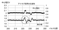
図5はこの手法により得られたアナログ信号Aの振幅の波形図を示し、データは600パルス/Rで、図1に示したような不連続部分11aが1回転で1個所、図5では230番目のパルス付近に現われている。
FIG. 5 shows a waveform diagram of the amplitude of the analog signal A obtained by this method. The data is 600 pulses / R, and the
このように、不連続部分11aが通過したとき信号振幅は低下することになるが、この低下のレベルとしては、4つのフォトダイオードS1〜S4を1セグメントとしたとき、図2では6セグメントのフォトダイオードのグループがあるのに対し、1セグメント分の信号が入力しないため、図5での信号レベルは不連続部分11aを設けないときの信号レベルと比べると5/6に低下している。
Thus, when the
マイクロコンピュータなどの演算処理部では、図5において信号レベルが3Vを下回った場合、又は振幅値が最小値になった場合などのときに原点であると認識し、そのときの位置を記憶し、或いはコンパレータを設けてパルス信号を出力する。 An arithmetic processing unit such as a microcomputer recognizes the origin when the signal level is lower than 3 V in FIG. 5 or when the amplitude value becomes the minimum value, and stores the position at that time. Alternatively, a pulse signal is output by providing a comparator.
このように、スケール11に不連続部分11aを設け、振幅を一方のデジタル信号DBのパルスエッジを基準に一方のアナログ信号Aをサンプリングし演算処理することで、原点位置を検出することが可能となる。
As described above, the
図6は本実施例1の原点検出アルゴリズムのフローチャート図である。ステップS1で原点検出を開始し、スケール11を移動させて信号を発生させる。
FIG. 6 is a flowchart of the origin detection algorithm of the first embodiment. In step S1, origin detection is started, and the
ステップS2でデジタル信号DBの立ち上りと立ち下りタイミングで、アナログ信号Aの信号を検出し、アナログ信号Aの最大値と最小値を求める。 In step S2, the analog signal A is detected at the rising and falling timings of the digital signal DB, and the maximum value and the minimum value of the analog signal A are obtained.
ステップS3で最大値−最小値を演算して振幅を求める。 In step S3, the maximum value-minimum value is calculated to determine the amplitude.
ステップS4で、振幅値が最小になる個所を検出する。 In step S4, a portion where the amplitude value is minimized is detected.
ステップS5で、振幅値が最小のパルス値のときのデジタル信号DAの立ち上り位置を原点とする。 In step S5, the rising position of the digital signal DA when the amplitude value is the minimum pulse value is set as the origin.
このようにして、デジタル信号の或る特定のパルスエッジを原点位置とすることにより、再現性の良い原点位置を高精度で得ることが可能となる。 Thus, by setting a specific pulse edge of the digital signal as the origin position, it is possible to obtain an origin position with good reproducibility with high accuracy.
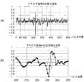
図7は実施例1において、検出不能となる場合の振幅変動の波形図を示している。スケール11に不連続部分11aを設けたにも拘らず、他の振幅変動が大きく、実施例1のような或る電圧を下廻ったとき、又は最小値となったときを計算しても、不連続部分11aを捉えられないという問題が発生することがある。
FIG. 7 shows a waveform diagram of amplitude fluctuation in the first embodiment when detection is impossible. Even if the
これはスケール11の汚れ、取付精度が悪いなどの原因によるものであるが、それを解消するためには、エンコーダを塵埃が侵入しない環境で使用したり、組み立て調整を厳しく行うなどの制約が生ずる。
This is due to factors such as dirt on the
本実施例2は振幅変動が大きくとも、スケール11の原点である不連続部分11aを検出するために、検出信号を微分して不連続部分11aが通過したときの急激な振幅変化を捉えている。
In the second embodiment, even if the amplitude fluctuation is large, in order to detect the
図8は図7におけるアナログ信号Aを微分した結果であり、図8(a)は全領域での微分信号の波形図、図8(b)は不連続部分11aが通過したときの振幅が急激に変化したときの微分信号の波形図を示している。
8 is a result of differentiating the analog signal A in FIG. 7, FIG. 8 (a) is a waveform diagram of the differential signal in the entire region, and FIG. 8 (b) is an abrupt amplitude when the
図8(a)から分かるように、スケール11の不連続部分11aが通過した個所では、微分値が大きく上下に変化している。これは実際の振幅が一瞬低下して直ちに復活するためである。図8(b)は微分値が大きく変化している個所の横軸を拡大しており、マークのある個所はエンコーダ信号の1パルスに相当する。
As can be seen from FIG. 8A, the differential value greatly changes up and down where the
ここで、マイクロコンピュータなどにより微分値を検索してゆき、例えば図8(b)で微分値が−0.5を下回った個所から、+0.5を超える間の個所で、最もゼロに近い値を見付けるようにする。すると、図8(b)の点線で囲った232番目のパルス位置が原点位置として選択できる。 Here, the differential value is searched by a microcomputer or the like. For example, the value closest to zero at the point where the differential value is below -0.5 to the point where it exceeds +0.5 in FIG. 8B. Try to find out. Then, the 232nd pulse position surrounded by the dotted line in FIG. 8B can be selected as the origin position.
従って、最初に計数したパルス計数値に対し232を差し引くなどして、以後はこのパルス位置を原点に決定することが可能となる。なお、この計数のときのデジタル信号DAのエッジを原点位置とすることで、精度の良い原点位置を得ることができる。 Accordingly, by subtracting 232 from the pulse count value initially counted, the pulse position can be determined as the origin thereafter. By setting the edge of the digital signal DA at the time of counting as the origin position, a precise origin position can be obtained.
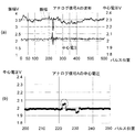
図9は実施例3を説明するためのアナログ信号Aの出力波形図であり、従来の信号振幅ではなく、アナログ信号Aの中心電圧に着目している。図9(a)は横軸をパルス位置としたときのアナログ信号Aの振幅とその中心電圧を示し、図9(b)はスケール11の不連続部分が通過する付近のアナログ信号Aの中心電圧の変化を横軸を拡大して示している。
FIG. 9 is an output waveform diagram of the analog signal A for explaining the third embodiment, and focuses on the center voltage of the analog signal A instead of the conventional signal amplitude. FIG. 9A shows the amplitude of the analog signal A and its center voltage when the horizontal axis is the pulse position, and FIG. 9B shows the center voltage of the analog signal A in the vicinity where the discontinuous portion of the
図9(b)から分かるように、アナログ信号Aの中心電圧はスケール11の不連続部分11aが発光部12、受光部13に入ったときにプラス側にピークを出力し、発光部12、受光部13を抜けるときにマイナス側にピークを出力する。
As can be seen from FIG. 9B, the center voltage of the analog signal A outputs a peak on the plus side when the
図10はこの現象の説明図であり、スケール11の不連続部分11aによる部分13bが受光部13の端の部分にあるとき、光が入射する部分と出射する部分で不均衡が生じ、図3の差動増幅器22で相殺していたオフセット成分が、微妙に発生している。これにより、図9(b)に示すような中心電圧の変化部が検出される。従って、図9(b)の点線でくくった個所のように、電圧変化のピークになるパルス位置を原点とすることができる。
FIG. 10 is an explanatory diagram of this phenomenon. When the
図9(a)からも分かるように、アナログ信号Aの中心電圧は、振幅が変化しているにも拘らず殆ど変化せず、スケール11の不連続部分11aが通過するときのみ変動するため、安定して原点を検出することが可能となる。
As can be seen from FIG. 9A, the center voltage of the analog signal A hardly changes despite the change in amplitude, and changes only when the
図11は実施例4のアナログ信号Aの中心電圧とその中心電圧を微分した波形を示している。この図11において、中心電圧のピークの部分を見ると、複数のピークが存在し、中心電圧のピークを取るという前述の実施例3では、状況により異なる方の個所が求めるピーク値になってしまうという問題が発生する。 FIG. 11 shows a center voltage of the analog signal A of the fourth embodiment and a waveform obtained by differentiating the center voltage. In FIG. 11, when looking at the peak portion of the center voltage, there are a plurality of peaks, and in the above-described third embodiment in which the peak of the center voltage is taken, a different portion depending on the situation has a desired peak value. The problem occurs.
そこで本実施例4では、アナログ信号Aの中心電圧の微分値を求めると、上がり下がりを有するS字カーブになるので、上昇してから下がるときのゼロに近い個所を原点と決定することで、確実に1個所を原点位置に決定することができる。なお図11においては、個所224番目のパルス位置が原点となる。 Therefore, in the fourth embodiment, when the differential value of the center voltage of the analog signal A is obtained, an S-shaped curve having an ascending / descending shape is obtained, and by determining a point close to zero when rising and descending as an origin, One place can be reliably determined as the origin position. In FIG. 11, the 224th pulse position is the origin.
また、ここで微分した結果の上がり下がりのゼロに近い個所が2個所あり、何れかを決められないとき、初期時にゼロに最も近い個所を原点として選択し、次の原点検出からは先の個所が持っていた値に最も近い個所を探すことにより、確実に原点位置を捉えることが可能となる。 In addition, there are two places where the result of differentiation here is close to zero in the rise and fall, and when either cannot be determined, the place closest to zero is selected as the origin at the initial stage, and the next place from the next origin detection By searching for the location closest to the value held by, the origin position can be reliably captured.
図12はこの実施例4の原点検出アルゴリズムのフローチャート図である。ステップS11で原点検出スタートし、スケール11を移動し信号を発生させる。ステップS12においてデジタル信号DBの立ち上りと立ち下りタイミングでアナログ信号Aの信号を検出することで、アナログ信号Aの最大値と最小値を検出する。
FIG. 12 is a flowchart of the origin detection algorithm of the fourth embodiment. In step S11, the origin detection starts, the
ステップS13で{最大値+最小値}/2から中心電圧を求める。ステップS14で中心電圧値データの中心電圧が或る値以上に変化している領域のデータを微分する。 In step S13, the center voltage is obtained from {maximum value + minimum value} / 2. In step S14, the data in the region where the center voltage of the center voltage value data changes to a certain value or more is differentiated.
ステップS15〜S16で初期測定のときは、微分値がゼロに近いパルス位置を原点と決定し、その微分値Xを記憶する。ステップS17で、初期測定ではないときは微分値がXのときの個所を選択する。ステップS18で、得られた個所のデジタル信号DAの立ち上りの位置を原点とする。 In the initial measurement in steps S15 to S16, a pulse position having a differential value close to zero is determined as the origin, and the differential value X is stored. In step S17, if it is not the initial measurement, the location where the differential value is X is selected. In step S18, the starting position of the obtained digital signal DA is set as the origin.
このようにして、デジタル信号の或る特定のパルスエッジを原点位置であるとすることにより、精度の良い原点位置を得ることが可能となる。 In this way, by setting a specific pulse edge of the digital signal as the origin position, it is possible to obtain a precise origin position.
11 スケール
11a 不連続部分
12 発光部
13 受光部
21 電流電圧変換器
22 差動増幅器
23 コンパレータ
S、S1〜S4 フォトダイオード
DESCRIPTION OF
Claims (5)
該スケールに対して相対移動可能に設けられ、光源から照射された光束を前記スケールを介して受光する複数の受光素子を1セグメントとし、複数の前記セグメントを有し、複数の前記セグメント間の互いに対応する位置からは同位相の出力が得られるよう前記光学格子のピッチに関係付けして配設した受光素子アレイと、
前記受光素子アレイから得られる電気信号に基づいてインクリメンタル信号を得る信号処理回路とを有する光学式エンコーダにおいて、
前記信号処理回路は、前記インクリメンタル信号として互いに位相が90°ずれた2つのアナログ信号と、前記2つのアナログ信号と位相が等しく、前記アナログ信号の2値化された信号である2つのデジタル信号とを出力し、
少なくとも一方のデジタル信号のパルスエッジのタイミングで得られる前記一方のデジタル信号と位相が90°ずれた前記アナログ信号の値に基づいて、前記位相が90°ずれたアナログ信号の振幅又は中心電圧を求め、前記不連続部材が前記受光素子アレイを通過するときに前記振幅又は前記中心電圧の変化を検出し、該変化が発生したときの位置に基づいて原点を検出することを特徴とする光学式エンコーダ。 An optical grating having a predetermined interval is formed, and a scale in which an optical discontinuity is provided in a part of the optical grating ;
A plurality of light receiving elements, which are provided so as to be movable relative to the scale and receive light beams emitted from a light source through the scale, are defined as one segment, have a plurality of the segments, and each other between the plurality of segments. A light receiving element array disposed in relation to the pitch of the optical grating so that an output of the same phase can be obtained from a corresponding position;
In an optical encoder having a signal processing circuit for obtaining an incremental signal based on an electric signal obtained from the light receiving element array,
The signal processing circuit includes two analog signals that are 90 ° out of phase with each other as the incremental signal, and two digital signals that are equal in phase to the two analog signals and are binarized signals of the analog signals. Output
Based on the value of the analog signal that is 90 ° out of phase with the one digital signal obtained at the timing of the pulse edge of at least one digital signal, the amplitude or center voltage of the analog signal that is 90 ° out of phase is obtained. , optical encoder, characterized in that the discontinuous member detects a change in the amplitude or the center voltage as it passes through the light-receiving element array, to detect the origin based on the position at which said change has occurred .
Priority Applications (3)
| Application Number | Priority Date | Filing Date | Title |
|---|---|---|---|
| JP2004177407A JP4498024B2 (en) | 2004-06-15 | 2004-06-15 | Optical encoder |
| US11/152,412 US7348544B2 (en) | 2004-06-15 | 2005-06-14 | Optical encoder with discontinuous optical grating |
| CN2005100779524A CN1712902B (en) | 2004-06-15 | 2005-06-15 | Optical encoder |
Applications Claiming Priority (1)
| Application Number | Priority Date | Filing Date | Title |
|---|---|---|---|
| JP2004177407A JP4498024B2 (en) | 2004-06-15 | 2004-06-15 | Optical encoder |
Publications (3)
| Publication Number | Publication Date |
|---|---|
| JP2006003126A JP2006003126A (en) | 2006-01-05 |
| JP2006003126A5 JP2006003126A5 (en) | 2007-07-26 |
| JP4498024B2 true JP4498024B2 (en) | 2010-07-07 |
Family
ID=35459538
Family Applications (1)
| Application Number | Title | Priority Date | Filing Date |
|---|---|---|---|
| JP2004177407A Expired - Fee Related JP4498024B2 (en) | 2004-06-15 | 2004-06-15 | Optical encoder |
Country Status (3)
| Country | Link |
|---|---|
| US (1) | US7348544B2 (en) |
| JP (1) | JP4498024B2 (en) |
| CN (1) | CN1712902B (en) |
Families Citing this family (22)
| Publication number | Priority date | Publication date | Assignee | Title |
|---|---|---|---|---|
| JP4908764B2 (en) * | 2005-02-04 | 2012-04-04 | キヤノン株式会社 | Optical encoder |
| JP4869628B2 (en) * | 2005-05-26 | 2012-02-08 | オリンパス株式会社 | Optical encoder |
| JP2008028025A (en) * | 2006-07-19 | 2008-02-07 | Canon Inc | Reflective sensor |
| JP4928206B2 (en) * | 2006-09-22 | 2012-05-09 | キヤノン株式会社 | Encoder |
| WO2008088650A1 (en) * | 2007-01-11 | 2008-07-24 | 3M Innovative Properties Company | Web longitudinal position sensor |
| CN101680780A (en) * | 2007-06-19 | 2010-03-24 | 3M创新有限公司 | Total internal reflection displacement scale |
| US8405831B2 (en) * | 2007-06-19 | 2013-03-26 | 3M Innovative Properties Company | Systems and methods for indicating the position of a web |
| JP2010530543A (en) * | 2007-06-19 | 2010-09-09 | スリーエム イノベイティブ プロパティズ カンパニー | System and method for manufacturing a displacement scale |
| US7965393B2 (en) | 2007-07-24 | 2011-06-21 | Mitutoyo Corporation | Reference signal generating configuration for an interferometric miniature grating encoder readhead using fiber optic receiver channels |
| US7973941B2 (en) * | 2007-07-24 | 2011-07-05 | Mitutoyo Corporation | Reference signal generating configuration for an interferometric miniature grating encoder readhead using fiber optic receiver channels |
| US7732754B2 (en) * | 2008-04-30 | 2010-06-08 | Avago Technologies Ecbu Ip (Singapore) Pte. Ltd. | Optical encoder with amplitude correction |
| US7709784B2 (en) * | 2008-04-30 | 2010-05-04 | Avago Technologies Ecbu Ip (Singapore) Pte. Ltd. | Optical encoder with code wheel misalignment detection and automatic gain control |
| US7834310B2 (en) * | 2008-06-23 | 2010-11-16 | Xerox Corporation | Position encoder's signal processing method and system |
| JP5113000B2 (en) * | 2008-09-19 | 2013-01-09 | 株式会社ミツトヨ | Photoelectric encoder |
| US8847185B2 (en) | 2008-12-29 | 2014-09-30 | 3M Innovative Properties Company | Phase-locked web position signal using web fiducials |
| CN102272375B (en) | 2008-12-30 | 2014-01-08 | 3M创新有限公司 | Apparatus and method for making fiducials on a substrate |
| JP5887064B2 (en) * | 2010-04-28 | 2016-03-16 | 株式会社ミツトヨ | Optical encoder |
| EP2386832B1 (en) * | 2010-05-10 | 2017-04-12 | Mitutoyo Corporation | Photoelectric encoder |
| JP5479255B2 (en) * | 2010-07-20 | 2014-04-23 | キヤノン株式会社 | Optical encoder |
| JP2014098666A (en) * | 2012-11-15 | 2014-05-29 | Canon Inc | Incremental encoder |
| WO2018079014A1 (en) * | 2016-10-25 | 2018-05-03 | 三菱電機株式会社 | Pulsing conversion device of incremental encoder, and pulsing conversion method |
| CN118354877A (en) * | 2021-12-20 | 2024-07-16 | 发那科株式会社 | A robot control device that performs zero point calibration by torque or force control |
Family Cites Families (21)
| Publication number | Priority date | Publication date | Assignee | Title |
|---|---|---|---|---|
| JPH0656304B2 (en) | 1989-09-05 | 1994-07-27 | 株式会社ミツトヨ | Photoelectric encoder |
| US5291133A (en) * | 1992-08-24 | 1994-03-01 | General Motors Corporation | Multi-bit encoder signal conditioning circuit having common mode disturbance compensation |
| JP3530573B2 (en) * | 1994-04-27 | 2004-05-24 | キヤノン株式会社 | Optical displacement sensor |
| JP3465483B2 (en) | 1996-06-26 | 2003-11-10 | ミノルタ株式会社 | Encoder device |
| US6201239B1 (en) * | 1997-01-21 | 2001-03-13 | Olympus Optical Co., Ltd. | Optical encoder |
| US5929789A (en) * | 1997-04-09 | 1999-07-27 | Hewlett-Packrd Company | Single channel incremental position encorder with incorporated reference mark |
| JPH10288538A (en) * | 1997-04-16 | 1998-10-27 | Sony Corp | Offset adjustment method |
| DE19830925A1 (en) * | 1997-08-07 | 1999-02-11 | Heidenhain Gmbh Dr Johannes | Sensing unit for optical position measurement |
| US6043483A (en) * | 1997-12-29 | 2000-03-28 | Radica China Limited | Apparatus and method using an indexed-encoder to sense the absolute position of an object with a single set of optics |
| EP1003012B3 (en) * | 1998-11-19 | 2011-04-20 | Dr. Johannes Heidenhain GmbH | Optical position measuring arrangement |
| US6396052B1 (en) * | 2000-04-07 | 2002-05-28 | Lexmark International, Inc. | High precision analog encoder system |
| US6713756B2 (en) * | 2000-05-09 | 2004-03-30 | Olympus Corporation | Optical encoder and optical rotary encoder |
| JP2001317963A (en) * | 2000-05-09 | 2001-11-16 | Olympus Optical Co Ltd | Optical encoder |
| JP4280447B2 (en) | 2001-02-20 | 2009-06-17 | キヤノン株式会社 | Reflection scale and displacement detection device using the same |
| US6660997B2 (en) * | 2001-04-26 | 2003-12-09 | Creo Srl | Absolute position Moiré type encoder for use in a control system |
| JP2003161645A (en) | 2001-11-28 | 2003-06-06 | Canon Inc | Optical encoder |
| JP4208483B2 (en) * | 2002-05-21 | 2009-01-14 | キヤノン株式会社 | Optical encoder |
| US7312437B2 (en) * | 2002-07-02 | 2007-12-25 | Olympus Corporation | Displacement sensor, method for detecting the optimal reference position, and method for judging stability of detecting the reference position of displacement sensor |
| US20040262502A1 (en) * | 2003-06-26 | 2004-12-30 | Xerox Corporation | Position encoder |
| US20050109924A1 (en) * | 2003-11-26 | 2005-05-26 | David Christenson | Apparatus for encoding and indexing |
| EP1577645B1 (en) * | 2004-03-17 | 2007-09-05 | Canon Kabushiki Kaisha | Optical encoder |
-
2004
- 2004-06-15 JP JP2004177407A patent/JP4498024B2/en not_active Expired - Fee Related
-
2005
- 2005-06-14 US US11/152,412 patent/US7348544B2/en not_active Expired - Fee Related
- 2005-06-15 CN CN2005100779524A patent/CN1712902B/en not_active Expired - Fee Related
Also Published As
| Publication number | Publication date |
|---|---|
| CN1712902B (en) | 2010-09-08 |
| US20050274880A1 (en) | 2005-12-15 |
| US7348544B2 (en) | 2008-03-25 |
| JP2006003126A (en) | 2006-01-05 |
| CN1712902A (en) | 2005-12-28 |
Similar Documents
| Publication | Publication Date | Title |
|---|---|---|
| JP4498024B2 (en) | Optical encoder | |
| US7425697B2 (en) | Origin detection method for optical encoder | |
| EP2006642A2 (en) | Absolute position encoder | |
| US20070018086A1 (en) | Optical Encoder | |
| US7391011B2 (en) | Optical encoder capable of detecting absolute position | |
| JP2003065803A (en) | Photoelectric encoder | |
| EP1688711B1 (en) | Optical encoder | |
| EP2803948B1 (en) | Reference signal generation apparatus and reference signal generation system | |
| US9534936B2 (en) | Reference signal generation apparatus and reference signal generation system | |
| KR0165222B1 (en) | Vertical displacement measurement device of x-y stage | |
| JP6694722B2 (en) | Optical encoder and its origin determination method | |
| EP0990870A1 (en) | Position sensor | |
| JP2000121316A (en) | Dimension measuring apparatus using optical scale | |
| EP2738523A2 (en) | Absolute encoder and method of obtaining absolute position | |
| JP2005291980A (en) | Optical encoder | |
| JP2005265512A (en) | Optical encoder | |
| JP2001041730A (en) | Linear scale | |
| JPH0933284A (en) | Optical encoder | |
| JP4945976B2 (en) | Optical absolute encoder | |
| JPH11271026A (en) | Dimension measuring apparatus using optical scale | |
| JP4693213B2 (en) | Apparatus and method for adjusting peak level of origin signal in linear scale | |
| JP2003106872A (en) | Device and method for detecting origin in linear sensor | |
| JP2012233755A (en) | Optical encoder and absolute position detecting method for the same | |
| JPH02103415A (en) | Photoelectric displacement detector |
Legal Events
| Date | Code | Title | Description |
|---|---|---|---|
| A521 | Request for written amendment filed |
Free format text: JAPANESE INTERMEDIATE CODE: A523 Effective date: 20070608 |
|
| A621 | Written request for application examination |
Free format text: JAPANESE INTERMEDIATE CODE: A621 Effective date: 20070608 |
|
| A977 | Report on retrieval |
Free format text: JAPANESE INTERMEDIATE CODE: A971007 Effective date: 20091021 |
|
| A131 | Notification of reasons for refusal |
Free format text: JAPANESE INTERMEDIATE CODE: A131 Effective date: 20091110 |
|
| A521 | Request for written amendment filed |
Free format text: JAPANESE INTERMEDIATE CODE: A523 Effective date: 20091224 |
|
| RD01 | Notification of change of attorney |
Free format text: JAPANESE INTERMEDIATE CODE: A7421 Effective date: 20100218 |
|
| TRDD | Decision of grant or rejection written | ||
| A01 | Written decision to grant a patent or to grant a registration (utility model) |
Free format text: JAPANESE INTERMEDIATE CODE: A01 Effective date: 20100406 |
|
| A01 | Written decision to grant a patent or to grant a registration (utility model) |
Free format text: JAPANESE INTERMEDIATE CODE: A01 |
|
| A61 | First payment of annual fees (during grant procedure) |
Free format text: JAPANESE INTERMEDIATE CODE: A61 Effective date: 20100413 |
|
| FPAY | Renewal fee payment (event date is renewal date of database) |
Free format text: PAYMENT UNTIL: 20130423 Year of fee payment: 3 |
|
| R150 | Certificate of patent or registration of utility model |
Ref document number: 4498024 Country of ref document: JP Free format text: JAPANESE INTERMEDIATE CODE: R150 Free format text: JAPANESE INTERMEDIATE CODE: R150 |
|
| FPAY | Renewal fee payment (event date is renewal date of database) |
Free format text: PAYMENT UNTIL: 20130423 Year of fee payment: 3 |
|
| FPAY | Renewal fee payment (event date is renewal date of database) |
Free format text: PAYMENT UNTIL: 20140423 Year of fee payment: 4 |
|
| LAPS | Cancellation because of no payment of annual fees |