JP2005291919A - Display probe inspection contact probe sheet and display panel inspection contact probe unit equipped with the display panel inspection contact probe sheet - Google Patents
Display probe inspection contact probe sheet and display panel inspection contact probe unit equipped with the display panel inspection contact probe sheet Download PDFInfo
- Publication number
- JP2005291919A JP2005291919A JP2004107362A JP2004107362A JP2005291919A JP 2005291919 A JP2005291919 A JP 2005291919A JP 2004107362 A JP2004107362 A JP 2004107362A JP 2004107362 A JP2004107362 A JP 2004107362A JP 2005291919 A JP2005291919 A JP 2005291919A
- Authority
- JP
- Japan
- Prior art keywords
- display panel
- contact probe
- contact
- probe sheet
- lead pattern
- Prior art date
- Legal status (The legal status is an assumption and is not a legal conclusion. Google has not performed a legal analysis and makes no representation as to the accuracy of the status listed.)
- Pending
Links
Images
Landscapes
- Electroluminescent Light Sources (AREA)
- Devices For Indicating Variable Information By Combining Individual Elements (AREA)
- Measuring Leads Or Probes (AREA)
- Testing Electric Properties And Detecting Electric Faults (AREA)
- Liquid Crystal (AREA)
Abstract
Description
本発明は、液晶パネルや有機ELパネルのような高精細映像・画像表示パネルの点灯試験等を行うために用いられる表示パネル検査用コンタクトプローブシート等に関するものである。 The present invention relates to a display panel inspection contact probe sheet and the like used for conducting a lighting test of a high-definition video / image display panel such as a liquid crystal panel or an organic EL panel.
液晶パネル外周縁部に引き出されて形成されたドライバIC等を搭載等するための多数の電極であってドライバIC等の搭載等の前は液晶パネルの検査用電極として使用される液晶パネルの各電極に通電させて、所定の試験を行うために使用する液晶パネル検査用プローブ部材として、例えば、可撓性基板にリードパターンが形成され、前記リードパターンにおける前記液晶パネルの各電極に接続する側に、前記リードパターンと電気的に接続された、前記液晶パネルの各電極に接触するためのバンプ接点(半球面形状をした接点)が設けられているプローブ部材が提案されている。ここで、バンプ接点としては、半球面形状をしたニッケルのコアに金メッキを施したものが用いられている(特許文献1、2)。
液晶パネルの各電極の配置は、例えば品種毎に異なる場合がある。そのため、検査用プローブ部材は、測定機に対して、取り外し可能に取り付けられる。しかし、近年、液晶パネルの電極が狭幅化するのに伴い、測定機の各配線(例えば中継用フレキシブル基板の配線)の狭幅化も進んでいる。そのため、近年、リードパターンと測定機の各配線との確実な接続や、前記リードパターンと前記測定機側の配線との位置合わせ接続が難しいという問題が生じている。
本発明は上記問題点に鑑みてなされたもめであり、表示パネル検査用コンタクトプローブシートの測定機側における前記リードパターンと前記測定機側の配線との確実な接続を実現でき、しかも前記リードパターンと前記測定機側の配線との位置合わせ接続が容易な表示パネル検査用コンタクトプローブシートの提供を目的とする。
The arrangement of the electrodes of the liquid crystal panel may differ depending on the product type, for example. Therefore, the inspection probe member is detachably attached to the measuring machine. However, in recent years, as the electrodes of the liquid crystal panel become narrower, the width of each wiring of the measuring instrument (for example, the wiring of the relay flexible substrate) is also progressing. Therefore, in recent years, there has been a problem that it is difficult to reliably connect the lead pattern and each wiring of the measuring instrument and to align and connect the lead pattern and the measuring instrument side wiring.
The present invention has been made in view of the above problems, and can realize a reliable connection between the lead pattern on the measuring instrument side of the contact probe sheet for display panel inspection and the wiring on the measuring instrument side, and the lead pattern. An object of the present invention is to provide a contact probe sheet for inspecting a display panel that can be easily aligned and connected to wiring on the measuring instrument side.
上記の課題を解決するために、本発明は、以下の構成を有する。
(構成1)本発明の構成1に係る発明は、表示パネルの各電極に通電させて、所定の試験を行うために使用する表示パネル検査用コンタクトプローブシートであって、上記試験を行う測定機と上記表示パネルとを電気的に接続するためのリードパターンであって、可撓性基板上に形成されたリードパターンと、上記リードパターンと、上記測定機側の配線とを電気的に接続するためのバンプ接点であって、上記可撓性基板における、上記リードパターンが形成されている面の反対側の面に形成されたバンプ接点とを備えることを特徴とする表示パネル検査用コンタクトプローブシートである。
上記構成1によれば、バンプ接点を用いることにより、リードパターンと、測定機側の配線との電気的接続を、確実に行うことができる。
なお、狭幅化・狭ピッチ化が進んだ場合、バンプ接点を介在させないで、表示パネル検査用コンタクトプローブシートの測定機側における前記リードパターンと前記測定機側の配線(リードパターン)とを直接接続すると、接続が不確実となる恐れがある。
例えば、バンプ接点を介在させないで、表示パネル検査用コンタクトプローブシートの測定機側におけるリードパターンと測定機側の配線とを直接接続しようとすると、確実な接続は難しい。これは、リードパターン及び配線の両方ともが微細な細線状であるため、両者を確実に重なり合わせるための位置合わせ接続が非常難しいためである。また、この場合、両者を接触面の全体に亘って十分に接触させなければ、十分な電気的接続を得られないため、わずかな誤差により、接続が不十分になってしまうおそれもある。
しかし、バンプ接点を用いた場合には、このバンプ接点を、測定機側の配線のいずれかの箇所に接触させればよいため、位置あわせが容易になる。例えば、リードパターンと測定機側の配線との間のピッチ等に多少のずれがあったとしても、バンプ接点による点接触であるため、位置合わせ接続が容易である。また、バンプ接点と配線とは、点で接触するため、確実に電気的接続させやすい。
In order to solve the above problems, the present invention has the following configuration.
(Configuration 1) The invention according to
According to the
In addition, when the narrowing and the narrow pitch are advanced, the lead pattern on the measuring instrument side of the contact probe sheet for display panel inspection and the wiring (lead pattern) on the measuring instrument side are directly connected without interposing a bump contact. If connected, the connection may be uncertain.
For example, if the lead pattern on the measuring instrument side of the contact probe sheet for display panel inspection and the wiring on the measuring instrument side are directly connected without interposing bump contacts, reliable connection is difficult. This is because both the lead pattern and the wiring are fine fine lines, and therefore it is very difficult to align and connect the two in order to reliably overlap them. Further, in this case, unless both are sufficiently brought into contact over the entire contact surface, a sufficient electrical connection cannot be obtained, and there is a possibility that the connection becomes insufficient due to a slight error.
However, when a bump contact is used, it is only necessary to bring this bump contact into contact with any part of the wiring on the measuring machine side, which facilitates alignment. For example, even if there is a slight deviation in the pitch between the lead pattern and the wiring on the measuring machine side, the contact is easy because of the point contact by the bump contact. Further, since the bump contact and the wiring are in contact with each other at a point, it is easy to reliably make an electrical connection.
ここで、近年、表示パネルの各電極パターンの幅・ピッチの狭幅化・狭ピッチ化に対応してコンタクトプローブシート上(可撓性基板上)に形成されたリードパターン(L&Sパターン)も狭幅化・狭ピッチ化している。また、これに伴い、コンタクトプローブシート上における測定機と接続される部分におけるリードパターンも狭幅化・狭ピッチ化している。
例えば、表示パネルの各電極と接続する側のライン幅(電極の幅)が50μm以下に狭幅化した場合、それと対応して、測定機側のリードパターン(L&Sパターン)のライン幅(電極の幅)は50μm以下に狭幅化する必要がある。また、ライン幅の狭幅化とともに、狭ピッチ化の傾向にある。
これに対し、本発明によれば、バンプ接点を用いることにより、測定機側のリードパターンのライン幅(電極の幅)が50μm以下に狭幅化した場合であっても、リードパターンと、測定機側の配線とを、隣の配線とショートせずに、確実に電気的に接続させることができる。したがって、本発明のコンタクトプローブシートは、表示パネルの各電極パターンのライン幅が50μm以下、前記測定機側のライン幅(電極の幅)が50μm以下のような表示パネルの検査に適している。
なお、バンプ接点は、例えばリードパターン上に重ねて形成することにより、リードパターンと同じ側に設けることも考えられる。しかし、この場合、バンプ接点の高さ等を制御するのが困難になり、バンプ接点の大きさにバラツキが生じてしまう。一方、本発明の構成においては、可撓性基板を挟んで、リードパターンとバンプ接点とを反対側に形成することにより、バンプ接点を、高い精度で形成することができる。
Here, in recent years, the lead pattern (L & S pattern) formed on the contact probe sheet (on the flexible substrate) corresponding to the narrowing and narrowing of the width and pitch of each electrode pattern of the display panel is also narrow. Width / narrow pitch. Along with this, the lead pattern in the portion connected to the measuring instrument on the contact probe sheet is also narrowed and narrowed.
For example, when the line width (electrode width) on the side connected to each electrode of the display panel is narrowed to 50 μm or less, correspondingly, the line width of the lead pattern (L & S pattern) on the measuring instrument side (electrode Width) needs to be narrowed to 50 μm or less. In addition, the line width tends to narrow and the pitch tends to narrow.
On the other hand, according to the present invention, even if the line width (electrode width) of the lead pattern on the measuring machine side is reduced to 50 μm or less by using the bump contact, the lead pattern and the measurement The machine-side wiring can be reliably electrically connected without short-circuiting with the adjacent wiring. Therefore, the contact probe sheet of the present invention is suitable for inspection of a display panel in which the line width of each electrode pattern of the display panel is 50 μm or less and the line width (electrode width) on the measuring instrument side is 50 μm or less.
It is also conceivable that the bump contact is provided on the same side as the lead pattern, for example, by overlapping it on the lead pattern. However, in this case, it becomes difficult to control the height of the bump contact, and the size of the bump contact varies. On the other hand, in the configuration of the present invention, the bump contact can be formed with high accuracy by forming the lead pattern and the bump contact on the opposite side across the flexible substrate.
(構成2)本発明の構成2に係る発明は、
上記リードパターンと、上記表示パネルの各電極とを電気的に接続するためのバンプ接点であって、上記可撓性基板における、上記リードパターンが形成されている面の反対側の面に形成されたバンプ接点を更に備えることを特徴とする構成1に記載の表示パネル検査用コンタクトプローブシートである。
上記構成2によれば、表示パネルの各電極に接触するためのバンプ接点も、可撓性基板をはさんでリードパターンと反対側に設けられる。この場合、可撓性基板は、表示パネル等とリードパターンとの間に配置される。そのため、例えば表示パネルを構成する基板からのガラス片等から、リードパターンを保護することができる。
また、この場合、表示パネルの各電極に接触するためのバンプ接点側と、可撓性基板を挟んで対向する辺に位置する測定機と接続するためのバンプ接点側との水平位置等を、フレキシブルな可撓性基板の屈曲によって、自由に設定可能となる。また中継用フレキシブル基板側を固定し、前記表示パネルの各電極に接触するためのバンプ接点側を昇降等させること可能となる。
(Configuration 2) The invention according to
A bump contact for electrically connecting the lead pattern and each electrode of the display panel, which is formed on a surface of the flexible substrate opposite to the surface on which the lead pattern is formed. The contact probe sheet for display panel inspection according to
According to the
In this case, the horizontal position of the bump contact side for contacting each electrode of the display panel and the bump contact side for connecting to a measuring machine located on the opposite side across the flexible substrate, etc. It can be freely set by bending the flexible substrate. In addition, it is possible to fix the relay flexible substrate side and raise and lower the bump contact side for contacting each electrode of the display panel.
(構成3)本発明の構成3に係る発明は、
上記バンプ接点の形状は、半球状であることを特徴とする上記構成1又は2記載の表示パネル検査用コンタクトプローブシートである。
上記構成3によれば、バンプ接点の形状を半球状とすることにより、測定機側の配線や表示パネル側の電極と点接触させることができ、異物が万が一介在されることによる接触不良を回避でき、又面接触する場合と比べて試験時の接触圧を低減できるので、被接触側のダメージも少ない。
(Configuration 3) The invention according to
3. The contact probe sheet for inspecting a display panel according to the
According to the
(構成4)本発明の構成4に係る発明は、
上記表示パネルは、液晶パネル又は有機ELパネルであることを特徴とする上記構成1乃至4の何れか一に記載の表示パネル検査用コンタクトプローブシートである。
上記構成4のように、本発明のコンタクトプローブシートは、表示パネルの各電極パターンのライン幅が50μm以下のような表示パネルの検査に適している。
(Configuration 4) The invention according to
5. The display panel inspection contact probe sheet according to
Like the said
本発明のコンタクトプローブシートは、高精細映像・画像表示パネルの各電極パターンのピッチが50μm以下の狭ピッチのものにおいて特に有効である。更には30μm以下のピッチの表示パネルでは更に有効である。このような高精細映像・画像表示パネルとしては、液晶パネル、有機ELパネル、プラズマディスプレイパネル等がある。 The contact probe sheet of the present invention is particularly effective when the pitch of each electrode pattern of a high-definition video / image display panel is a narrow pitch of 50 μm or less. Furthermore, it is more effective for a display panel having a pitch of 30 μm or less. Such high-definition video / image display panels include liquid crystal panels, organic EL panels, plasma display panels, and the like.
(構成5)本発明の構成5に係る発明は、
上記構成1乃至4の何れか一に記載の表示パネル検査用コンタクトプローブシートと、前記コンタクトプローブシートにおける少なくとも前記表示パネルの各電極に接続する側を載置し支持するための支持台と、を有することを特徴とする表示パネル検査用コンタクトプローブユニットである。
上記構成5によれば、リードパターンと、測定機側の配線との電気的接続を、確実に行うことができる表示パネル検査用コンタクトプローブシートを具備した表示パネル検査用コンタクトプローブユニットを提供できる。
(Configuration 5) The invention according to Configuration 5 of the present invention is
The contact probe sheet for display panel inspection according to any one of the
According to the configuration 5, it is possible to provide a display panel inspection contact probe unit including a display panel inspection contact probe sheet capable of reliably performing electrical connection between the lead pattern and the measuring instrument side wiring.
本発明によれば、表示パネル検査用コンタクトプローブシートの測定機側におけるリードパターンと測定機側の配線との確実な接続を実現できる。
また、本発明の表示パネル検査用コンタクトプローブシートに適した表示パネル検査用コンタクトプローブユニットを提供できる。
ADVANTAGE OF THE INVENTION According to this invention, the reliable connection of the lead pattern in the measuring instrument side of the contact probe sheet for a display panel test | inspection, and the wiring by the measuring instrument side is realizable.
Moreover, a display panel inspection contact probe unit suitable for the display panel inspection contact probe sheet of the present invention can be provided.
以下、本発明を実施するための形態について説明する。
まず、本発明の液晶パネル検査用コンタクトプローブシートについて説明する。
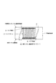
本発明の液晶パネル検査用コンタクトプローブシート10は、図1の一実施形態に示すように、
可撓性基板1上に形成されたリードパターン2と、バンプ接点3とを備える。リードパターン2は、試験を行う測定機と表示パネルとを電気的に接続するための配線である。バンプ接点3は、リードパターン2と接続された端子であり、液晶パネル検査用コンタクトプローブシート10における、中継用フレキシブル基板接続側と、表示パネル接続側とに設けられている。そして、中継用フレキシブル基板接続側のバンプ接点3は、リードパターン2と、上記測定機側の配線とを電気的に接続する。そして、このバンプ接点3は、可撓性基板1における、リードパターン2が形成されている面の反対側の面(可撓性基板1を挟んでリードパターン2と反対側)に形成されている(構成1)。尚、中継用フレキシブル基板は、測定機側の配線の一例である。
また、本発明において、上記構成2で述べたように、表示パネル接続側のバンプ接点3は、リードパターン2と、表示パネルの各電極とを電気的に接続する。そして、このバンプ接点3は、可撓性基板1における、リードパターン2が形成されている面の反対側の面に形成されているのが好ましい。中継用フレキシブル基板接続側及び表示パネル接続側のバンプ接点3は、可撓性基板1に設けられたスルーホールを介して、リードパターン2と接続される。
Hereinafter, modes for carrying out the present invention will be described.
First, the liquid crystal panel inspection contact probe sheet of the present invention will be described.
The
A
In the present invention, as described in the
本発明において、可撓性基板の材料としては、ポリイミド系樹脂、ポリエステル系樹脂、エポキシ系樹脂、ウレタン系樹脂、ポリスチレン系樹脂、ポリエチレン系樹脂、ポリアミド系樹脂、ABS系樹脂、ポリカーポネート系樹脂、シリコーン系樹脂などが挙げられる。可撓性基板の厚さは任意に選択できるが、十分な機械的強度や可撓性を有するようにするため、通常、2μm〜500μmの範囲で設定する。
リードパターン、及びリードパターンとバンプ接点とを接続するための材料としては、導電性を有するものであれば特に限定されないが、公知の良導体金属が好ましい。例えば、銅、金、銀、白金、鉛、錫、ニッケル、鉄、コバルト、インジウム、ロジウム、クロム、タングステン、ルテニウムなどの単体金属、またはこれらを成分とする各種合金、などが挙げられる。
リードパターンを形成する方法としては、可撓性基板の全面に導電性材料層を形成し、目的の回路パターンを残すように他の部分をエッチング等により除去する方法等が挙げられる。
In the present invention, the material of the flexible substrate includes polyimide resin, polyester resin, epoxy resin, urethane resin, polystyrene resin, polyethylene resin, polyamide resin, ABS resin, and polycarbonate resin. And silicone resins. The thickness of the flexible substrate can be arbitrarily selected, but is usually set in the range of 2 μm to 500 μm in order to have sufficient mechanical strength and flexibility.
The material for connecting the lead pattern and the lead pattern to the bump contact is not particularly limited as long as it has conductivity, but a known good conductor metal is preferable. Examples thereof include simple metals such as copper, gold, silver, platinum, lead, tin, nickel, iron, cobalt, indium, rhodium, chromium, tungsten, ruthenium, and various alloys containing these as components.
Examples of the method for forming the lead pattern include a method in which a conductive material layer is formed on the entire surface of the flexible substrate, and other portions are removed by etching or the like so as to leave a target circuit pattern.
リードパターンとバンプ接点とを連通させ電気的に接続するための可撓性基板に形成されるスルーホールの孔径は限定されないが、隣り合ったスルーホール同士が繋がらない程度まで大きくすることによって、導通部の電気抵抗を小さくできるので好ましい。スルーホールの実用的な孔径は、5μm〜200μmである。表示パネルの検査に使用するコンタクトプローブシートの場合、5μm〜20μmとすることが好ましい。スルーホールの形成方法としては、レーザー加工法、フォトリソグラフィー法、プラズマ加工法、パンチングなどの機械的加工、などの方法が挙げられる。これらの方法の中でも、エキシマレーザー、炭酸ガスレーザー、YAGレーザーなどによるレーザー加工は、スルーホールを任意の孔径や孔間ピッチにて微細加工が可能であり、バンプ接点のファインピッチ化に対応でき、好ましい方法である。
また、リードパターンとバンプ接点とを電気的に接続するため手段としては、スルーホール内に導電性物質を充填してなるもの、スルーホールメッキのように貫通孔の壁面に導電性物質の層を形成してなるものなどがある。形成方法としては、電気メッキ法や無電解メッキ法、CVD法などの成膜方法、機械的に導電性物質をスルーホール内に嵌め込む方法、なとが挙げられる。これらの方法の中でもスルーホール内にリードパターンの一部を構成する材料を露出させ、この材料を負極として電気メッキによってスルーホール内に導電性物質を充填する方法が、確実な導通が得られ、かつ簡便であるので好ましい。
また、バンプ接点の形状は、可撓性基板面からの突出の有無を問わず、接触対象物の形状や材料に応じて、凸状、凹状、平坦パッド状、どのような形状であっても良いが、半球状に突起したものが最も有用である。ここでいう半球状とは完全な半球だけではなく、単調な曲面を持って突起した形状を含む。バンプ接点は複数としても良く、その個数、配置等は限定されない。
The hole diameter of the through hole formed in the flexible substrate for connecting and electrically connecting the lead pattern and the bump contact is not limited, but it is made conductive by increasing it to the extent that adjacent through holes are not connected to each other. This is preferable because the electrical resistance of the portion can be reduced. The practical hole diameter of the through hole is 5 μm to 200 μm. In the case of a contact probe sheet used for inspection of a display panel, the thickness is preferably 5 μm to 20 μm. Examples of the through hole forming method include laser processing, photolithography, plasma processing, and mechanical processing such as punching. Among these methods, laser processing with excimer laser, carbon dioxide gas laser, YAG laser, etc. can finely process through holes with any hole diameter and pitch between holes, and can cope with fine pitch of bump contacts, This is the preferred method.
In addition, as means for electrically connecting the lead pattern and the bump contact, the through hole is filled with a conductive material, and a layer of a conductive material is formed on the wall surface of the through hole like through-hole plating. Some are formed. Examples of the forming method include a film forming method such as an electroplating method, an electroless plating method, and a CVD method, and a method of mechanically fitting a conductive substance into the through hole. Among these methods, a method of exposing a material constituting a part of the lead pattern in the through hole and filling the through hole with a conductive substance by electroplating using this material as a negative electrode provides reliable conduction, And it is preferable because it is simple.
In addition, the shape of the bump contact may be any shape such as a convex shape, a concave shape, a flat pad shape, depending on the shape and material of the contact object, regardless of whether or not it protrudes from the surface of the flexible substrate. Although good, a hemispherical protrusion is most useful. Here, the hemispherical shape includes not only a perfect hemisphere but also a protruding shape having a monotonous curved surface. There may be a plurality of bump contacts, and the number, arrangement, etc. thereof are not limited.
また、本発明においては、バンプ接点を、金属と炭素を含む材料で構成することにより、バンプ接点を構成する結晶の粒径が小さくなることで、バンプ接点表面の表面粗さを小さくすることができる。これに加え、各金属結晶の粒界に炭素が集中することで硬度が高くなるか、または、金属の結晶の間に硬度が高い金属の炭化物が入りこみバンプ接点全体として硬度が高くなるので、コンタクトプローブシートの寿命が飛躍的に向上する。また、この場合、中継用フレキシブル基板における配線や、表示パネルの電極に対するダメージを防止することができる。バンプ接点を構成する金属としては、Niが好ましい。金属としてNiを用いた場合、バンプ接点中に含まれる炭素は、ニッケルカーバイドの形で存在する。
なお、中継用フレキシブル基板接続側のバンプ接点3の材料と、表示パネル接続側のバンプ接点3の材料とは、同じにした方が好ましい。その材料は、導電性を有する他のもの(例えば金属又は合金)であってよい。
In the present invention, the bump contact is made of a material containing metal and carbon, so that the grain size of the crystals constituting the bump contact is reduced, thereby reducing the surface roughness of the bump contact surface. it can. In addition to this, the hardness increases due to the concentration of carbon at the grain boundaries of each metal crystal, or the hardness of the bump contact as a whole increases due to the high hardness of the metal carbide entering between the metal crystals. The life of the probe sheet is dramatically improved. Further, in this case, it is possible to prevent damage to the wiring on the relay flexible substrate and the electrodes of the display panel. Ni is preferable as the metal constituting the bump contact. When Ni is used as the metal, the carbon contained in the bump contact exists in the form of nickel carbide.
The material of the
バンプ接点中に炭素を含有させる方法としては、メッキ溶液中にメッキ溶液に溶解する有機物質を入れ、メッキ条件を調整することによってできる。メッキ溶液中にいれる有機物質としては、メッキ溶液に溶解する有機物質であって、バンプ接点を電気メッキ法等で製造する際に、バンプ接点に炭素が取り込まれる作用を有する有機物質であれば良い。例えば、炭酸(H2CO3)、二酸化炭素(CO2)、サンカリン、ショ糖、ブドウ糖などであっても良い。 As a method for containing carbon in the bump contact, an organic substance that dissolves in the plating solution is placed in the plating solution, and the plating conditions are adjusted. The organic substance contained in the plating solution may be an organic substance that dissolves in the plating solution and has an action of incorporating carbon into the bump contact when the bump contact is manufactured by an electroplating method or the like. . For example, carbonic acid (H 2 CO 3 ), carbon dioxide (CO 2 ), sankaline, sucrose, glucose and the like may be used.
また、バンプ接点表面には、金メッキを形成してもよい。金メッキはNi等からなるコアバンプと比べ柔らかい材料であり、また、金の電気伝導性(電気的接触性)によって、1バンプ接点当たりの加重を従来の1/2〜1/3に低減することができるため、中継用フレキシブル基板におけるフレキ配線や、表示パネルの電極に対するダメージを防止することができる。金メッキの条件、厚さ、表面粗さ等は、上記作用効果が効果的に得られるように調整する。 Further, gold plating may be formed on the bump contact surface. Gold plating is a softer material than core bumps made of Ni or the like, and the electrical conductivity (electrical contact) of gold can reduce the load per bump contact to 1/2 to 1/3 of the conventional one. Therefore, it is possible to prevent damage to the flexible wiring in the relay flexible substrate and the electrodes of the display panel. The conditions, thickness, surface roughness, etc. of the gold plating are adjusted so that the above effects can be obtained effectively.
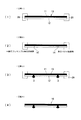
次に、本発明の表示パネル検査用コンタクトプローブシートの製造方法について、図2を参照して説明する。
(工程1):まず、銅箔11とポリイミドフィルム12とを積層した構造のフィルム13を張力が均一に係った状態で固定治具20に固定する(図2(1))。
(工程2):次に、銅箔11を周知のリソグラフィー法でエッチングしてリードパターンを形成した後、液晶パネルの電極と接続する側に表示パネルの電極のピッチと同じピッチ(約40μm)でエキシマレーザーにより、ポリイミドフィルム12に直径約10μmのスルーホール14を形成する。
また、液晶パネルの電極と接続する側とは反対側である、中継用フレキシブル基板と接続する側に、中継用フレキシブル基板の配線パターンと同じピッチ(約80μm)でエキシマレーザーによりポリイミドフィルムに直径約10μmのスルーホール14’を形成する(図2(2))。
(工程3):次に、表面側の銅箔面(リードパターン側の面)がメッキされないように保護した後、銅箔11(各リードパターン)の一部にそれぞれメッキ用電極を持続し、スルーホール内に露出した銅箔を負極として、ニッケルと炭素を含むニッケル合金の電気メッキを行う。
ニッケル合金をスルーホール内に析出させて充填し、さらに析出を継続して、ポリイミド面12’から約10μm突出した高さまで半球状に成長させて、バンプ接点3を形成した(図2(3))。尚、電気メッキの際に、メッキ液へ強度増強剤及び応力緩和剤を添加するとともに、メッキ条件並びに硬度増強剤及び応力緩和剤の量を調整することによって、バンプ接点3を構成する材料の結晶粒径を制御して、バンプ接点3表面の表面粗さを制御(鏡面化)した。
(工程4):最後に、固定治具20から積層構造フィルム13を外して液晶パネル検査用コンタクトプローブシート10を作製する(図2(4))。
Next, the manufacturing method of the contact probe sheet | seat for a display panel test | inspection of this invention is demonstrated with reference to FIG.
(Step 1): First, the
(Step 2): Next, after the
Also, on the side connected to the flexible substrate for relay, which is opposite to the side connected to the electrode of the liquid crystal panel, the diameter of the polyimide film is approximately the same as the wiring pattern of the flexible substrate for relay (about 80 μm) by excimer laser. A 10 μm through
(Step 3): Next, after protecting the copper foil surface on the surface side (surface on the lead pattern side) from being plated, the plating electrode is maintained on a part of the copper foil 11 (each lead pattern), Electroplating of a nickel alloy containing nickel and carbon is performed using the copper foil exposed in the through hole as a negative electrode.
The nickel alloy was deposited and filled in the through hole, and further the deposition was continued to grow hemispherically to a height protruding about 10 μm from the
(Step 4): Finally, the
次に、本発明の表示パネル検査用コンタクトプローブユニットについて説明する。
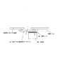
本発明の表示パネル検査用コンタクトプローブユニットは、図3の一実施形態に示すように、表示パネル検査用コンタクトプローブシート10と、前記コンタクトプローブシート10における少なくとも前記表示パネルの各電極に接続する側を載置し支持するための支持台(シートを固定させる筐体)30と、を有する。
支持台おける少なくとも前記表示パネルの各電極に接続する側を載置し支持する面は、平坦(好ましくは±5μm程度)とすることが好ましい。支持台の材質はアルミニウム、SUSなどが好ましい。
表示パネル検査用コンタクトプローブシート10と支持台30との間には、弾性シート(シリコンゴムシート)40を介在させることが好ましい。弾性シートとプローブシートとの間は接着する必要はなくプローブシートの交換が容易である。
表示パネル検査用コンタクトプローブシート10を、支持台30上の所定位置に位置決め固定するためには、例えば、支持台30上の所定位置に位置決め用のピンを設け、このピンに表示パネル検査用コンタクトプローブシート10に設けた穴を通す手段が簡便でありしかも高位置精度が実現できる。プローブシートの交換も容易である。
また、表示パネル検査用コンタクトプローブシート10及び支持台30に、それぞれアライメントマークを設け、表示パネル検査用コンタクトプローブシートを、支持台上の所定位置に位置決め固定することもできる。
表示パネル検査用コンタクトプローブシート及び支持台には、それぞれ、表示パネル側のアライメントマークと位置あわせするためのアライメントマークを設けることができる。
Next, the display panel inspection contact probe unit of the present invention will be described.
The display panel inspection contact probe unit of the present invention includes a display panel inspection
It is preferable that the surface of the support base on which at least the side connected to each electrode of the display panel is placed and supported is flat (preferably about ± 5 μm). The material of the support base is preferably aluminum or SUS.
An elastic sheet (silicon rubber sheet) 40 is preferably interposed between the display panel inspection
In order to position and fix the display panel inspection
In addition, the display panel inspection
Each of the display panel inspection contact probe sheet and the support base may be provided with an alignment mark for alignment with the alignment mark on the display panel side.
本発明の液晶パネル検査用コンタクトプローブユニットは、前記支持台に載置された前記コンタクトプローブシートを狭持し固定するための抑え具、を有することが好ましい。
これは、前記支持台に載置されたコンタクトプローブシートを抑え具により上方から狭持することによって、繰り返しコンタクトさせた場合であってもコンタクトプローブシートに位置ずれ等を生じさせず、確実且つ安定的な表示パネル検査用コンタクトプローブユニットを提供できるからである。
また、支持台30は、昇降機構及び加圧機構等で駆動することによって、表示パネルの検査を行う。この場合、支持台30は、表示パネル検査用コンタクトプローブシート10における、表示パネル(例えば液晶パネル)に近い部分のみを昇降させてよい。この場合、中継用フレキシブル基板における配線と、中継用フレキシブル基板側のバンプ接点とは、一旦位置あわせされて接続した後は、接続を保持する。
上記構成によれば、コンタクトプローブシート10の測定機側におけるリードパターンと測定機の配線とをバンプ接点を介在させて接続を行うことによって、測定機とコンタクトプローブシート10との電気的接続を、確実に行うことができる。
The contact probe unit for inspecting a liquid crystal panel of the present invention preferably has a pressing member for sandwiching and fixing the contact probe sheet placed on the support base.
This is because the contact probe sheet placed on the support base is sandwiched from above by a holding tool so that the contact probe sheet is not misaligned even if it is repeatedly contacted, and it is reliable and stable. This is because a typical contact probe unit for display panel inspection can be provided.
Moreover, the support base 30 inspects the display panel by being driven by an elevating mechanism and a pressurizing mechanism. In this case, the support base 30 may raise and lower only the portion close to the display panel (for example, a liquid crystal panel) in the display panel inspection
According to the above configuration, by connecting the lead pattern on the measuring instrument side of the
次に、本発明の実施例について説明する。
(実施例1)
上述の液晶パネル検査用コンタクトプローブシートの製造方法により、ポリイミドフィルムと鋼箔とを積層した構造の2層フィルム(ポリイミド膜厚12.5μm、鋼箔厚5μm)を用い、銅からなるリードパターンのピッチが約40μm、リードパターンの線幅が約25μm、リードパターンの裏面に形成されたニッケルと炭素とを含むバンプ接点(中継用フレキシブル基板側、表示パネル側)のバンプ径(直径)が約30μm、高さが約10μmの液晶パネル検査用コンタクトプローブシートを作製した。(図1態様)
上記で得られたコンタクトプローブシートをコンタクトプローブユニットを介して液晶パネル検査装置に装着し、有機ELパネルの検査を行った。
なお、液晶パネル検査装置は測定機の一例である。また、検査に先立ち、液晶パネル検査装置の配線である中継フレキ配線とバンプ接点とを接触させて抑え具により固定した。
有機ELパネルの検査を10万回行った後、コンタクトプローブシートをコンタクトプローブユニットから取り外した。
10万回の検査の間、中継フレキ配線とバンプ接点とは良好に接触していた。そのため、液晶パネル検査装置と、コンタクトプローブシートとの電気的接続は良好であり、問題は生じなかった。また、バンプ接点の加圧接触によって接続していた中継用フレキシブル基板上の各配線パターン、表示パネル側の各電極を顕微鏡で観察したが、ダメージは形成されていなかった。
コンタクトプローブシートを新しいものに交換し、有機ELパネルの検査を行った。検査10万回毎に、コンタクトプローブシートを新しいものに10回交換し、有機ELパネルの検査を100万回行ったが、液晶パネル検査装置と、コンタクトプローブシートとの電気的接続は常に良好であった。また、中継用フレキシブル基板の配線とバンプ接点でショートは発生しなかった。また、中継用フレキシブル基板上の各配線パターンには顕微鏡観察によるダメージは形成されておらず、中継用フレキシブル基板の交換は不要であった。
Next, examples of the present invention will be described.
(Example 1)
By using the above-described method for manufacturing a contact probe sheet for inspecting a liquid crystal panel, a two-layer film (polyimide film thickness 12.5 μm, steel foil thickness 5 μm) having a structure in which a polyimide film and a steel foil are laminated is used. The pitch is about 40 μm, the line width of the lead pattern is about 25 μm, and the bump diameter (diameter) of the bump contact (nickel flexible substrate side, display panel side) including nickel and carbon formed on the back surface of the lead pattern is about 30 μm. A contact probe sheet for liquid crystal panel inspection having a height of about 10 μm was prepared. (Aspect of FIG. 1)
The contact probe sheet obtained above was attached to a liquid crystal panel inspection apparatus via a contact probe unit, and an organic EL panel was inspected.
The liquid crystal panel inspection apparatus is an example of a measuring machine. Prior to the inspection, the relay flexible wiring, which is the wiring of the liquid crystal panel inspection apparatus, and the bump contact were brought into contact with each other and fixed with a suppressor.
After the organic EL panel was inspected 100,000 times, the contact probe sheet was removed from the contact probe unit.
The relay flexible wiring and the bump contact were in good contact during the 100,000 inspections. Therefore, the electrical connection between the liquid crystal panel inspection apparatus and the contact probe sheet was good, and no problem occurred. Moreover, although each wiring pattern on the flexible substrate for relay and each electrode on the display panel side that were connected by the pressure contact of the bump contact were observed with a microscope, no damage was formed.
The contact probe sheet was replaced with a new one, and the organic EL panel was inspected. Every 100,000 inspections, the contact probe sheet was replaced with a
(実施例2)
実施例1のバンプ接点表面に、厚さ0.1nm〜0.2nmの金メッキを形成した以外は実施例1と同様にして液晶パネル検査用コンタクトプローブシートを作製した。実施例1と同様にして、検査10万回毎に、コンタクトプローブシートを新しいものに10回交換し、有機ELパネルの検査を100万回行った。
この場合も、液晶パネル検査装置と、コンタクトプローブシートとの電気的接続は常に良好であった。また、中継用フレキシブル基板の配線とバンプ接点でショートは発生しなかった。また、中継用フレキシブル基板上の各配線パターンには顕微鏡観察によるダメージは形成されておらず、中継用フレキシブル基板の交換は不要であった。
(Example 2)
A contact probe sheet for inspecting a liquid crystal panel was produced in the same manner as in Example 1 except that gold plating having a thickness of 0.1 nm to 0.2 nm was formed on the bump contact surface of Example 1. In the same manner as in Example 1, every 100,000 inspections, the contact probe sheet was replaced with a
Also in this case, the electrical connection between the liquid crystal panel inspection apparatus and the contact probe sheet was always good. Further, no short circuit occurred between the wiring of the relay flexible board and the bump contact. Further, no damage was observed in each wiring pattern on the relay flexible substrate by microscopic observation, and it was not necessary to replace the relay flexible substrate.
(比較例)
実施例1のコンタクトプローブシートにおいて、中継用フレキシブル基板側にバンプ接点を形成せず、リードパターンと、中継用フレキシブル基板の配線とを、接着剤により固定した。また、コンタクトプローブシートの交換は、接着剤用剥離液を用いて行った。
上記以外は実施例1と同様にして、有機ELパネルの検査を行った。また、検査10万回毎に、コンタクトプローブシートを新しいものに交換した。
この場合、コンタクトプローブシートの交換により、リードパターンと、中継用フレキシブル基板の配線とが、異物等の介在や、リードパターンが隣の配線と接触するなどで、適切に接触しなくなり、液晶パネル検査装置と、コンタクトプローブシートとの電気的接続が不良になる場合があった。また、30万回の検査の時点で、中継用フレキシブル基板の配線に接触不良が発生し、中継用フレキシブル基板を交換しなければ検査を続けることができなかった。
(Comparative example)
In the contact probe sheet of Example 1, bump contacts were not formed on the relay flexible substrate side, and the lead pattern and the wiring of the relay flexible substrate were fixed with an adhesive. Further, the contact probe sheet was exchanged using an adhesive stripping solution.
Other than the above, the organic EL panel was inspected in the same manner as in Example 1. In addition, the contact probe sheet was replaced with a new one every 100,000 inspections.
In this case, by replacing the contact probe sheet, the lead pattern and the wiring of the relay flexible board are not properly in contact with each other due to the presence of foreign matters or the lead pattern coming into contact with the adjacent wiring. In some cases, the electrical connection between the apparatus and the contact probe sheet is poor. Further, at the time of the inspection of 300,000 times, a contact failure occurred in the wiring of the relay flexible substrate, and the inspection could not be continued unless the relay flexible substrate was replaced.
以上の実施例及び比較例の結果から、実施例のように、コンタクトプローブシートと中継用フレキシブル基板とを、可撓性基板を挟んでリードパターンと反対側に形成されたバンプ接点により接続させることにより、表示パネル検査用コンタクトプローブシートの測定機側におけるリードパターンと測定機側の配線との確実な接続を実現できる。また、中継用フレキシブル基板の配線に対するダメージを防止することができるため、中継用フレキシブル基板を長期間に亘って使用することができる。 From the results of the above examples and comparative examples, as in the examples, the contact probe sheet and the relay flexible substrate are connected by the bump contact formed on the opposite side of the lead pattern across the flexible substrate. Thus, it is possible to realize a reliable connection between the lead pattern on the measuring instrument side of the contact probe sheet for inspecting the display panel and the wiring on the measuring instrument side. Moreover, since the damage with respect to the wiring of the flexible substrate for relay can be prevented, the flexible substrate for relay can be used over a long period of time.
1 可撓性基板
2 リードパターン
3 バンプ接点
10 表示パネル検査用コンタクトプローブシート
30 支持台
DESCRIPTION OF
Claims (5)
前記試験を行う測定機と前記表示パネルとを電気的に接続するためのリードパターンであって、可撓性基板上に形成されたリードパターンと、
前記リードパターンと、前記測定機側の配線とを電気的に接続するためのバンプ接点であって、前記可撓性基板における、前記リードパターンが形成されている面の反対側の面に形成されたバンプ接点と
を備えることを特徴とする表示パネル検査用コンタクトプローブシート。 A contact probe sheet for inspecting a display panel used for conducting a predetermined test by energizing each electrode of the display panel,
A lead pattern for electrically connecting the measuring instrument for performing the test and the display panel, wherein the lead pattern is formed on a flexible substrate;
A bump contact for electrically connecting the lead pattern and the wiring on the measuring instrument side, formed on the surface of the flexible substrate opposite to the surface on which the lead pattern is formed. A contact probe sheet for inspecting a display panel, comprising a bump contact.
Priority Applications (1)
| Application Number | Priority Date | Filing Date | Title |
|---|---|---|---|
| JP2004107362A JP2005291919A (en) | 2004-03-31 | 2004-03-31 | Display probe inspection contact probe sheet and display panel inspection contact probe unit equipped with the display panel inspection contact probe sheet |
Applications Claiming Priority (1)
| Application Number | Priority Date | Filing Date | Title |
|---|---|---|---|
| JP2004107362A JP2005291919A (en) | 2004-03-31 | 2004-03-31 | Display probe inspection contact probe sheet and display panel inspection contact probe unit equipped with the display panel inspection contact probe sheet |
Publications (1)
| Publication Number | Publication Date |
|---|---|
| JP2005291919A true JP2005291919A (en) | 2005-10-20 |
Family
ID=35325007
Family Applications (1)
| Application Number | Title | Priority Date | Filing Date |
|---|---|---|---|
| JP2004107362A Pending JP2005291919A (en) | 2004-03-31 | 2004-03-31 | Display probe inspection contact probe sheet and display panel inspection contact probe unit equipped with the display panel inspection contact probe sheet |
Country Status (1)
| Country | Link |
|---|---|
| JP (1) | JP2005291919A (en) |
-
2004
- 2004-03-31 JP JP2004107362A patent/JP2005291919A/en active Pending
Similar Documents
| Publication | Publication Date | Title |
|---|---|---|
| KR100801395B1 (en) | Manufacturing method of probe sheet | |
| KR0150334B1 (en) | Probe card having vertical needle | |
| JP4465995B2 (en) | Probe sheet, probe card, semiconductor inspection apparatus, and semiconductor device manufacturing method | |
| JP5918205B2 (en) | Test apparatus and test method thereof | |
| JP2010276541A (en) | Thin film probe sheet and manufacturing method thereof, probe card, and semiconductor chip inspection apparatus | |
| WO2000010016A1 (en) | Contactor and production method for contactor | |
| JP3976276B2 (en) | Inspection device | |
| JP4107275B2 (en) | Inspection probe and inspection apparatus, and inspection probe manufacturing method | |
| KR200471838Y1 (en) | Needle Type Pin Board for Small Size Liquid Crystal Panel | |
| JP2008244069A (en) | Display device, COF manufacturing method | |
| JP4246097B2 (en) | Display probe inspection contact probe sheet and display panel inspection contact probe unit equipped with the display panel inspection contact probe sheet | |
| JP2009098153A (en) | Method for manufacturing thin film probe | |
| JPH10206464A (en) | Probe device | |
| JP4246096B2 (en) | Display probe inspection contact probe sheet and display panel inspection contact probe unit equipped with the display panel inspection contact probe sheet | |
| JP2005291919A (en) | Display probe inspection contact probe sheet and display panel inspection contact probe unit equipped with the display panel inspection contact probe sheet | |
| JP4246558B2 (en) | Wiring substrate for probe and method for manufacturing semiconductor element | |
| JP2006337229A (en) | Probe for current test | |
| JPH1194910A (en) | Probe inspection device | |
| JP2004132699A (en) | Connecting apparatus, semiconductor chip inspecting apparatus, and method for manufacturing the connecting apparatus | |
| JP2006071486A (en) | CONNECTION DEVICE, SEMICONDUCTOR CHIP INSPECTION DEVICE, AND SEMICONDUCTOR DEVICE MANUFACTURING METHOD | |
| KR101578831B1 (en) | Driving film for testing display panel and method for producing thereof | |
| JP4185225B2 (en) | Contact probe inspection system | |
| JP3090132B2 (en) | Method of manufacturing probe head | |
| JP2005016959A (en) | Display panel inspection device | |
| JPH11352151A (en) | Contact probe, probe device having the same, and method of manufacturing contact probe |
Legal Events
| Date | Code | Title | Description |
|---|---|---|---|
| A621 | Written request for application examination |
Free format text: JAPANESE INTERMEDIATE CODE: A621 Effective date: 20070323 |
|
| A977 | Report on retrieval |
Free format text: JAPANESE INTERMEDIATE CODE: A971007 Effective date: 20090624 |
|
| A131 | Notification of reasons for refusal |
Free format text: JAPANESE INTERMEDIATE CODE: A131 Effective date: 20090630 |
|
| A521 | Request for written amendment filed |
Free format text: JAPANESE INTERMEDIATE CODE: A523 Effective date: 20090831 |
|
| A131 | Notification of reasons for refusal |
Free format text: JAPANESE INTERMEDIATE CODE: A131 Effective date: 20090929 |
|
| A02 | Decision of refusal |
Free format text: JAPANESE INTERMEDIATE CODE: A02 Effective date: 20100209 |