JP2005291870A - Microchannel module - Google Patents
Microchannel module Download PDFInfo
- Publication number
- JP2005291870A JP2005291870A JP2004106276A JP2004106276A JP2005291870A JP 2005291870 A JP2005291870 A JP 2005291870A JP 2004106276 A JP2004106276 A JP 2004106276A JP 2004106276 A JP2004106276 A JP 2004106276A JP 2005291870 A JP2005291870 A JP 2005291870A
- Authority
- JP
- Japan
- Prior art keywords
- glass
- microchannel module
- pair
- sample
- channel
- Prior art date
- Legal status (The legal status is an assumption and is not a legal conclusion. Google has not performed a legal analysis and makes no representation as to the accuracy of the status listed.)
- Withdrawn
Links
- 239000011521 glass Substances 0.000 claims abstract description 41
- 239000007853 buffer solution Substances 0.000 claims description 12
- BASFCYQUMIYNBI-UHFFFAOYSA-N platinum Chemical compound [Pt] BASFCYQUMIYNBI-UHFFFAOYSA-N 0.000 claims description 12
- 238000002347 injection Methods 0.000 claims description 10
- 239000007924 injection Substances 0.000 claims description 10
- 229910052697 platinum Inorganic materials 0.000 claims description 6
- VYZAMTAEIAYCRO-UHFFFAOYSA-N Chromium Chemical compound [Cr] VYZAMTAEIAYCRO-UHFFFAOYSA-N 0.000 claims description 5
- 238000000034 method Methods 0.000 claims description 5
- 238000004544 sputter deposition Methods 0.000 claims description 5
- 229910052804 chromium Inorganic materials 0.000 claims description 4
- 239000011651 chromium Substances 0.000 claims description 4
- 238000001997 free-flow electrophoresis Methods 0.000 claims description 4
- 239000000758 substrate Substances 0.000 abstract description 10
- 238000001962 electrophoresis Methods 0.000 abstract description 4
- 239000007788 liquid Substances 0.000 abstract description 4
- 238000004519 manufacturing process Methods 0.000 abstract description 3
- 239000000872 buffer Substances 0.000 abstract description 2
- 230000037431 insertion Effects 0.000 abstract 1
- 238000003780 insertion Methods 0.000 abstract 1
- 239000005357 flat glass Substances 0.000 description 4
- XUIMIQQOPSSXEZ-UHFFFAOYSA-N Silicon Chemical compound [Si] XUIMIQQOPSSXEZ-UHFFFAOYSA-N 0.000 description 3
- 239000012460 protein solution Substances 0.000 description 3
- 229910052710 silicon Inorganic materials 0.000 description 3
- 239000010703 silicon Substances 0.000 description 3
- 239000000853 adhesive Substances 0.000 description 2
- 230000001070 adhesive effect Effects 0.000 description 2
- 150000001413 amino acids Chemical class 0.000 description 2
- 238000004891 communication Methods 0.000 description 2
- 238000013461 design Methods 0.000 description 2
- 230000020169 heat generation Effects 0.000 description 2
- 238000012545 processing Methods 0.000 description 2
- 238000000926 separation method Methods 0.000 description 2
- 239000010409 thin film Substances 0.000 description 2
- 238000007792 addition Methods 0.000 description 1
- 238000010276 construction Methods 0.000 description 1
- 238000011161 development Methods 0.000 description 1
- 238000010438 heat treatment Methods 0.000 description 1
- 238000012986 modification Methods 0.000 description 1
- 230000004048 modification Effects 0.000 description 1
- 102000004169 proteins and genes Human genes 0.000 description 1
- 108090000623 proteins and genes Proteins 0.000 description 1
- 238000011160 research Methods 0.000 description 1
- 229910001220 stainless steel Inorganic materials 0.000 description 1
- 239000010935 stainless steel Substances 0.000 description 1
- 238000011144 upstream manufacturing Methods 0.000 description 1
- 239000002699 waste material Substances 0.000 description 1
Images

Landscapes
- Electrostatic Separation (AREA)
- Micromachines (AREA)
Abstract
Description
本発明は、2枚の平行平板間で形成されるチャンネルの長手方向にバッファー液と共に試料を供給し、平行平板の幅方向両端に設けた1対の電極による電位差で試料を泳動させて試料の成分を分離するフリーフロー型電気泳動のためのマイクロチャンネルモジュールに関する。 In the present invention, a sample is supplied together with a buffer solution in the longitudinal direction of a channel formed between two parallel flat plates, and the sample is electrophoresed by a potential difference between a pair of electrodes provided at both ends of the parallel flat plate in the width direction. The present invention relates to a microchannel module for free-flow electrophoresis for separating components.
2枚の平行平板間で形成されるチャンネルの長手方向にバッファー液と共に試料を供給し、平行平板の幅方向両端に設けた1対の電極による電位差で試料を泳動させて試料の成分を分離するフリーフロー型電気泳動装置は既に知られている。このフリーフロー型電気泳動装置は連続して多数の試料を取り扱えて便利であるが、チャンネルの間隙を大きくすると高電圧を要し、電流の増大と温度上昇により、バッファー液から揮発ガスが生じ、その後ガス成分の一部が凝縮することで電気泳動作用の監視を困難にさせるために、1mm程度に抑えていた(特許文献1参照)。 A sample is supplied together with a buffer solution in the longitudinal direction of a channel formed between two parallel flat plates, and the sample components are separated by migrating the sample by a potential difference between a pair of electrodes provided at both ends of the parallel flat plate in the width direction. Free flow type electrophoresis apparatuses are already known. This free-flow type electrophoresis apparatus is convenient because it can handle a large number of samples continuously, but if the gap between the channels is increased, a high voltage is required. Due to the increase in current and temperature, volatile gas is generated from the buffer solution, Thereafter, in order to make it difficult to monitor the electrophoretic action by condensing a part of the gas component, the gas component is suppressed to about 1 mm (see Patent Document 1).
このような技術上の背景に基づき、試料が流れるチャンネル間隙を1mmより更に小さく設定できれば、微小電力で駆動でき、ガスの発生も抑えられるという観点からマイクロ化の研究が進められているが、平行な微細流路の加工は困難でありコスト高になる欠点があるので、低電力でも試料の分離が正確に行われるようなバッファー液の開発が活発化しているのが現状である。 Based on this technical background, if the gap between the channels through which the sample flows can be set to be smaller than 1 mm, research into microfabrication is underway from the viewpoint that it can be driven with minute electric power and gas generation can be suppressed. Since the processing of such fine channels is difficult and costly, there is a current situation that the development of a buffer solution that can accurately separate the sample even at low power is being activated.
本発明は、このような事情に基づいてなされたもので、およそ100μm〜50μm程度のチャンネル間隙を低コストで製作できるマイクロチャンネルモジュールを提供することを目的とするものである。 The present invention has been made based on such circumstances, and an object of the present invention is to provide a microchannel module capable of manufacturing a channel gap of about 100 μm to 50 μm at a low cost.
上記の目的を解決するために、本発明の請求項1に記載のマイクロチャンネルモジュールは、2枚の平行平板間で形成されるチャンネルの長手方向にバッファー液と共に試料を供給し、平行平板の幅方向両端に設けた1対の電極による電位差で試料を泳動させて試料の成分を分離するフリーフロー型電気泳動のためのマイクロチャンネルモジュールであって、該モジュールは一対のガラス体を接合して形成され、一方のガラス体に凸状体を形成するとともに、他方のガラス体に前記凸状体を囲繞する凹状体を形成し、前記凸状体頂面と凹状体の底面と間で微細間隙のチャンネルを構成したことを特徴としている。
この特徴によれば、微細間隙をガラス体に直接形成するのでなく、一方のガラス体に凸状部を、他方のガラス体に凹状部を形成して、凸状部と凹状部の高さの差を利用して微細間隙を形成するのでマイクロチャンネルの形成が容易である。
In order to solve the above object, a microchannel module according to
According to this feature, the minute gap is not formed directly in the glass body, but a convex portion is formed in one glass body, and a concave portion is formed in the other glass body. Since the fine gap is formed using the difference, the microchannel can be easily formed.
本発明の請求項2に記載のマイクロチャンネルモジュールは、請求項1に記載のマイクロチャンネルモジュールであって、前記一対のガラス体の接合を陽極接合法で行うことを特徴としている。
この特徴によれば、陽極接合法で熱膨張係数が等しいガラス体同士を接合するので、接合面の精度の向上が図れる。
A microchannel module according to a second aspect of the present invention is the microchannel module according to the first aspect, wherein the pair of glass bodies are bonded by an anodic bonding method.
According to this feature, since the glass bodies having the same thermal expansion coefficient are joined by the anodic bonding method, the accuracy of the joining surface can be improved.
本発明の請求項3に記載のマイクロチャンネルモジュールは、請求項1または2に記載のマイクロチャンネルモジュールであって、1対の電極を一対のガラス体のどちらか一方に形成したことを特徴としている。
この特徴によれば、ガラス体のどちら側にも選択的に設けることができるので、モジュール設計の容易化が図れる。
A microchannel module according to a third aspect of the present invention is the microchannel module according to the first or second aspect, wherein a pair of electrodes is formed on one of a pair of glass bodies. .
According to this feature, the module design can be facilitated because it can be selectively provided on either side of the glass body.
本発明の請求項4に記載のマイクロチャンネルモジュールは、請求項1ないし3のいずれかに記載のマイクロチャンネルモジュールであって、前記1対の電極は白金電極であり、ガラス体に対してクロム層を介してスパッタリング法で接合したことを特徴としている。
この特徴によれば、スパッタリング法でクロム層を介して白金電極をガラス体に接合するので、接着強度が大きく薄膜に形成できガラス体同士の接合に障害とならない。
A microchannel module according to a fourth aspect of the present invention is the microchannel module according to any one of the first to third aspects, wherein the pair of electrodes are platinum electrodes, and a chromium layer is formed on the glass body. It is characterized by being joined by a sputtering method.
According to this feature, since the platinum electrode is bonded to the glass body through the chromium layer by a sputtering method, the adhesive strength can be increased to form a thin film, which does not hinder the bonding of the glass bodies.
本発明の請求項5に記載のマイクロチャンネルモジュールは、請求項1ないし4の何れかに記載のマイクロチャンネルモジュールであって、前記ガラス体にはチャンネルの一端側に連通する注入用のガラス配管が、他端側に分取用のガラス配管が設けられていることを特徴としている。
この特徴によれば、ガラス体にガラス配管を設けることで、液漏れのない通路を形成することができる。
A microchannel module according to a fifth aspect of the present invention is the microchannel module according to any one of the first to fourth aspects, wherein the glass body has a glass pipe for injection communicating with one end side of the channel. Further, a glass pipe for sorting is provided on the other end side.
According to this feature, by providing the glass pipe on the glass body, a passage without liquid leakage can be formed.
本発明の請求項6に記載のマイクロチャンネルモジュールは、請求項1ないし5の何れかに記載のマイクロチャンネルモジュールであって、前記チャンネルの間隙が100μm〜50μmであることを特徴としている。
この特徴によれば、チャンネルの間隙が100μm〜50μmであるモジュールを製作することで、マイクロ化の利点、即ち微少電力、低発熱が図れ、少ない試料で分離が可能で、使用後の廃棄物の量も少なくすることができる。
A microchannel module according to a sixth aspect of the present invention is the microchannel module according to any one of the first to fifth aspects, wherein the gap between the channels is 100 μm to 50 μm.
According to this feature, by manufacturing a module with a channel gap of 100 μm to 50 μm, the advantage of micro-processing, that is, low power and low heat generation can be achieved, and separation with a small number of samples is possible. The amount can also be reduced.
本発明の実施例を以下に説明する。 Examples of the present invention will be described below.
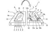
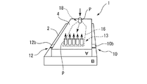
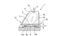
図1〜図5は、本発明の一実施形態を示すもので、図1は本発明に係るマイクロチャンネルモジュールの基部と蓋部を展開した状態を示す分解斜視図、図2は白金電極部の拡大断面図、図3は組立てられたマイクロチャンネルモジュールの全体斜視図、図4は組立てられたマイクロチャンネルモジュールの内部構造を示す断面図であり、図5(a)、(b)は流路を形成するための説明図である。 1 to 5 show an embodiment of the present invention. FIG. 1 is an exploded perspective view showing a state in which a base portion and a lid portion of a microchannel module according to the present invention are developed, and FIG. 3 is an enlarged perspective view, FIG. 3 is an overall perspective view of the assembled microchannel module, FIG. 4 is a sectional view showing the internal structure of the assembled microchannel module, and FIGS. 5A and 5B show flow paths. It is explanatory drawing for forming.
図1に示す符号1は、マイクロチャンネルモジュールを示し、このマイクロチャンネルモジュール1は、互いに接合される接合面間に微細な偏平空隙となる後述する流動室(チャンネル)を形成する平板状のガラス体で構成される基板2と蓋板4とから成り、基板2の上面内方には頂面が平坦な平面で外形が五角形となる凸状体5が形成されると共に、蓋板4の上面内方には底面が平坦な平面で外形が前記凸状体5に挿嵌可能な五角形となる凹状体6が形成されている。
基板2の凸状体5を囲む周囲には平坦な接合面2aが形成され、左右両側辺が下辺に対し垂直で且つ平行に形成される凸状体5の前方には、その頂面5aと下面を連通するサンプル注入ポート8が形成されている。
A
また、凸状体5の両側頂面には、両側辺に沿って延設される所定長さの1対の偏平な陰、陽の内部電極10a,12aと、これら両内部電極10a,12aの中央部から凸状体5両側の両接合面2aの端部まで延びる陰、陽の外部電極10b,12bとから成る陰、陽電極10,12が配設されている。
Further, a pair of flat negative and positive
そして、これらの陰、陽電極10,12は、図2に示すように、凸状体を構成するガラス体2に対してクロム層14を介して白金電極15がスパッタリング法によって接合されている。このように、スパッタリング法により接合することで、接着強度が大きくなり薄膜に形成できるのでガラス体同士の接合の障害とならない。尚、陰、陽電極10,12は、凸状体5に限らず凹状体6に設けることも可能であり、どちら側のガラス体にも選択的に設けることでモジュール設計が容易となる。
As shown in FIG. 2, these negative and
一方、蓋板4の凹状体6を囲む周囲には平坦な接合面4aが形成され、凹状体6の下辺側には、底面6aと下面を連通する5つの連通孔から成る分取ポート13が形成されると共に三角形状の凹状体6先端には、凹状体6の底面6aと下面を連通するバッファー液注入ポート18が形成されている。
On the other hand, a
そして、凸状体5のサンプル注入ポート8、及び凹状体6の分取ポート13、バッファー液注入ポート18には所定長さのガラス管Pがそれぞれ溶着される。このように、各ポート8,13,18にガラス管Pを設けることで、液漏れのない通路を形成することができる。
A glass tube P having a predetermined length is welded to the sample injection port 8 of the
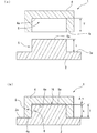
次に、マイクロチャンネルモジュール1の接合される接合面間に微細な偏平空隙となる流動室(チャンネル)の形成方法に付き図5(a)、(b)を参照して説明する。
Next, a method for forming a flow chamber (channel) that forms a fine flat gap between the joining surfaces to which the
図5(a)に示すように、板厚10mm前後の平板状ガラス体から成る基板2の上面には、接合面2aを基準として平行平坦な頂面5aまでの高さtの凸状体5を加工すると共に、同程度の板厚を有する平板状ガラス体から成る蓋板4の上面には、接合面4aを基準として平行平坦な底面6aまでの深さTの凹状体6が凸状体5に挿嵌可能な形状に正確に加工される。
As shown in FIG. 5A, on the upper surface of the
そこで、基板2の凸状体5に蓋板4の凹状体6を挿嵌させて接合面2a,4aを接合させると、凸状体5の頂面5aと凹状体6の底面6aとの間に微細な平行間隙T−t=Δt(図4参照)が約100μm〜50μmになるように形成する。尚、間隙Δtが50μmの場合の許容誤差は±5μmである。
Accordingly, when the
ここで、基板2と蓋板4を構成する平板状のガラス体は、熱膨張熱膨張係数が等しいガラス体であって、これらガラス体の基板2と蓋板4の接合には、両ガラス体間にシリコンを挟んでにヒータでシリコンを500℃程度に加熱することでシリコン表面を酸化させて接合する陽極接合法を採用することで、接合面精度の向上を図ることができる。
Here, the flat glass bodies constituting the
次に、前述した実施例で説明した構成のマイクロチャンネルモジュールを使用して試料の成分を分離するフリーフロー電気泳動に付き説明する。 Next, a description will be given of free flow electrophoresis in which the components of the sample are separated using the microchannel module having the configuration described in the above-described embodiment.
図3に示すように、ガラス体によって構成される基板2と蓋板4の接合により一体化されたマイクロチャンネルモジュール1は、分取ポート13の5つの連通孔に装着された各ガラス管Pに例えばステンレス製の管を介して図示しない吸引ポンプを接続する。
As shown in FIG. 3, the
次に、バッファー液をガラス管Pを介してバッファー液注入ポート18から偏平空隙となるチャンネル16内に注入し吸引ポンプを作動させることで、バッファー液は100μm〜50μm程度の偏平空隙のチャンネル16内に上流から下流の分取ポート13に向く矢印方向の流れが形成される。
Next, the buffer solution is injected into the
そこで、陰、陽電極10,12に電圧を印加すると電荷が形成され、基板2下面のガラス管Pを介してサンプル注入ポート8からサンプル(試料)として、例えばタンパク質溶液がチャンネル16内に注入されると、タンパク質溶液中の電荷を帯びた成分(アミノ酸)は、陰、陽電極10,12による電位差で泳動して試料の成分が分離される。すなわち、タンパク質溶液中の電荷とゲル状のバッファー液の流れとによって、タンパク質は陽極電極12側へ、アミノ酸は陰極電極10側にひかれて泳動分離されながら分取ポート13へと排出される。
Therefore, when a voltage is applied to the negative and
従って、チャンネル16の偏平空隙の間隙が100μm〜50μmであるモジュール1を製作することで、マイクロ化の利点、即ち微少電力、低発熱が図れ、少ないサンプルで分離が可能で、使用後の廃棄物の量も少なくすることができる。
Therefore, by producing the
以上、本発明の実施例を図面により説明してきたが、具体的な構成はこれら実施例に限られるものではなく、本発明の要旨を逸脱しない範囲における変更や追加があっても本発明に含まれる。 Although the embodiments of the present invention have been described with reference to the drawings, the specific configuration is not limited to these embodiments, and modifications and additions within the scope of the present invention are included in the present invention. It is.
1 マイクロチャンネルモジュール
2 基板
2a 接合面
4 蓋板
4a 接合面
5 凸状体
5a 頂面
6 凹状体
6a 底面
8 サンプル注入ポート
10b,12b 外部電極
10a,12a 内部電極
10,12 陰、陽電極
13 分取ポート
14 クロム層
15 白金電極
16 チャンネル
18 バッファー液注入ポート
P ガラス管
Δt 間隙
DESCRIPTION OF
Claims (6)
Priority Applications (1)
| Application Number | Priority Date | Filing Date | Title |
|---|---|---|---|
| JP2004106276A JP2005291870A (en) | 2004-03-31 | 2004-03-31 | Microchannel module |
Applications Claiming Priority (1)
| Application Number | Priority Date | Filing Date | Title |
|---|---|---|---|
| JP2004106276A JP2005291870A (en) | 2004-03-31 | 2004-03-31 | Microchannel module |
Publications (1)
| Publication Number | Publication Date |
|---|---|
| JP2005291870A true JP2005291870A (en) | 2005-10-20 |
Family
ID=35324963
Family Applications (1)
| Application Number | Title | Priority Date | Filing Date |
|---|---|---|---|
| JP2004106276A Withdrawn JP2005291870A (en) | 2004-03-31 | 2004-03-31 | Microchannel module |
Country Status (1)
| Country | Link |
|---|---|
| JP (1) | JP2005291870A (en) |
Cited By (4)
| Publication number | Priority date | Publication date | Assignee | Title |
|---|---|---|---|---|
| KR100854160B1 (en) * | 2002-08-28 | 2008-08-26 | 가부시끼가이샤 도시바 | Display device |
| JP2008249346A (en) * | 2007-03-29 | 2008-10-16 | National Institute Of Advanced Industrial & Technology | Microchip manufacturing method and microchip |
| JP5120968B2 (en) * | 2007-10-05 | 2013-01-16 | 国立大学法人九州工業大学 | Dielectrophoresis apparatus and method |
| CN103386253A (en) * | 2013-06-28 | 2013-11-13 | 上海交通大学 | Multi-hose flow-direction controller for free-flow electrophoresis apparatus |
-
2004
- 2004-03-31 JP JP2004106276A patent/JP2005291870A/en not_active Withdrawn
Cited By (5)
| Publication number | Priority date | Publication date | Assignee | Title |
|---|---|---|---|---|
| KR100854160B1 (en) * | 2002-08-28 | 2008-08-26 | 가부시끼가이샤 도시바 | Display device |
| JP2008249346A (en) * | 2007-03-29 | 2008-10-16 | National Institute Of Advanced Industrial & Technology | Microchip manufacturing method and microchip |
| JP5120968B2 (en) * | 2007-10-05 | 2013-01-16 | 国立大学法人九州工業大学 | Dielectrophoresis apparatus and method |
| US8864972B2 (en) | 2007-10-05 | 2014-10-21 | Kyushu Institute Of Technology | Dielectrophoresis apparatus and method |
| CN103386253A (en) * | 2013-06-28 | 2013-11-13 | 上海交通大学 | Multi-hose flow-direction controller for free-flow electrophoresis apparatus |
Similar Documents
| Publication | Publication Date | Title |
|---|---|---|
| Xu et al. | Room-temperature imprinting method for plastic microchannel fabrication | |
| Kohlheyer et al. | Free-flow zone electrophoresis and isoelectric focusing using a microfabricated glass device with ion permeable membranes | |
| JP4656149B2 (en) | Flow cell and manufacturing method thereof | |
| Duffy et al. | Rapid prototyping of microfluidic systems in poly (dimethylsiloxane) | |
| US9512421B1 (en) | Miniature acoustic wave lysis system and uses thereof | |
| CN101561446A (en) | Glass micro-nano-fluidic control chip, preparation and assembly method and auxiliary assembly device thereof | |
| JP3866183B2 (en) | Biochip | |
| Preuss et al. | Miniaturized free‐flow electrophoresis: production, optimization, and application using 3D printing technology | |
| JP2005291870A (en) | Microchannel module | |
| JP2002310858A (en) | Sample introduction method in microchip electrophoresis | |
| CN111849764A (en) | Microfluidic chip for multiplex separation of exosome samples | |
| JP3847414B2 (en) | Electrophoresis device | |
| CN102507708A (en) | Chip-type thin-layer electrolytic cell capillary electrophoresis microfluidic online sample feeding device | |
| JP2004340758A (en) | Microchannel and microchemical chip containing the same | |
| JPH11337521A (en) | Electrophoresis components | |
| TWI417531B (en) | Dielectrophoresis particle concentrator and concentration and detection method | |
| Baek et al. | A laser-micromachined PCB electrolytic micropump using an oil-based electrolyte separation barrier | |
| JPH09210960A (en) | Capillary electrophoresis device | |
| JP2010190211A (en) | Jointed body and fluid device | |
| JP5723198B2 (en) | Fluid handling device and fluid handling system | |
| JP2002214193A (en) | Minute passage element | |
| JP2005055320A (en) | Electrophoresis chip | |
| US8815069B2 (en) | Disposable capillary electrophoresis detecting device | |
| JP7258203B2 (en) | microfluidic device | |
| JP4670713B2 (en) | Cell electrophysiological sensor and cell electrophysiological measurement method using the same |
Legal Events
| Date | Code | Title | Description |
|---|---|---|---|
| A621 | Written request for application examination |
Free format text: JAPANESE INTERMEDIATE CODE: A621 Effective date: 20051104 |
|
| A761 | Written withdrawal of application |
Free format text: JAPANESE INTERMEDIATE CODE: A761 Effective date: 20070720 |