JP2005274156A - Flaw inspection device - Google Patents
Flaw inspection device Download PDFInfo
- Publication number
- JP2005274156A JP2005274156A JP2004083569A JP2004083569A JP2005274156A JP 2005274156 A JP2005274156 A JP 2005274156A JP 2004083569 A JP2004083569 A JP 2004083569A JP 2004083569 A JP2004083569 A JP 2004083569A JP 2005274156 A JP2005274156 A JP 2005274156A
- Authority
- JP
- Japan
- Prior art keywords
- subject
- image
- imaging
- wavelength
- defect
- Prior art date
- Legal status (The legal status is an assumption and is not a legal conclusion. Google has not performed a legal analysis and makes no representation as to the accuracy of the status listed.)
- Pending
Links
Images


Landscapes
- Length Measuring Devices By Optical Means (AREA)
- Investigating Materials By The Use Of Optical Means Adapted For Particular Applications (AREA)
- Testing Or Measuring Of Semiconductors Or The Like (AREA)
Abstract
Description
本発明は、被検査対象物の欠陥を検出する欠陥検査装置に関している。 The present invention relates to a defect inspection apparatus for detecting a defect of an object to be inspected.
従来、半導体等の基板を製造する際に、前記基板上には、種々の原因により欠陥が形成されてしまう場合がある。例えば、フォトリソグラフィ・プロセスにおいての基板表面に塗布されたレジストの膜厚むらや、前記レジストに付着した塵埃は、欠陥の原因になる。前記欠陥には、例えば、エッチング後の基板上の周期パターンの線幅不良や、前記パターン内のピンホールなどがある。また、パターンの露光においての合焦不良は、現像後のレジストの断面形状の形成不良の欠陥の原因となる。この欠陥は、後工程においての不良の原因となり得る。 Conventionally, when a substrate such as a semiconductor is manufactured, defects may be formed on the substrate due to various causes. For example, uneven thickness of the resist applied to the substrate surface in the photolithography process and dust adhering to the resist cause defects. Examples of the defect include a defective line width of a periodic pattern on a substrate after etching, a pinhole in the pattern, and the like. In addition, a poor focus in pattern exposure causes a defect in formation of a cross-sectional shape of a resist after development. This defect can cause a defect in a later process.
このため、前記ウェハや基板等は、欠陥検出並びに欠陥を修正が行われる。なお、前記欠陥を検出するために、欠陥検査装置が、一般的に用いられている。 For this reason, the wafer and the substrate are subjected to defect detection and defect correction. In order to detect the defect, a defect inspection apparatus is generally used.
例えば、前記従来の欠陥検査装置は、特許文献1並びに2に示されている。この特許文献1の従来の欠陥検査装置を、以下で、図10を参照して説明し、特許文献2の従来の欠陥検査装置を、図11を参照して説明する。
For example,
特許文献1の欠陥検査装置は、少なくとも1つの周期パターンを有する前記ウェハや基板等の被検体101により正反射した光束を観測し、被検体101上の欠陥を検出する装置である。具体的には、この欠陥検査装置は、ランプハウス5を具備している。このランプハウス5は、ハロゲンランプ6と、コンデンサレンズ7と、熱吸収フィルタ8とを有している。ハロゲンランプ6からの光は、熱吸収フィルタ8を介してコンデンサレンズ7に入射し、平行光束に変換される。
The defect inspection apparatus of
この欠陥検査装置は、さらに複数の干渉フィルタと、白色光照明用の孔とを有する回転ホルダ9を具備している。この回転ホルダ9は、回転することにより、任意の前記干渉フィルタ又は前記孔を、コンデンサレンズ7を通過した光束の光路上に配置し得るように、構成されている。また、前記各干渉フィルタは、所定の波長を中心とした所定の帯域の光束のみを透過し得るように構成されている。このため、回転ホルダ9は、干渉フィルタを変更することにより、通過する光束の波長幅を任意に変更し得る。なお、本明細書中において、所定の波長幅を有する光束において、前記波長幅の中心の波長を、中心波長と呼ぶ。
The defect inspection apparatus further includes a rotating holder 9 having a plurality of interference filters and a white light illumination hole. The rotating holder 9 is configured so that any interference filter or the hole can be arranged on the optical path of the light beam that has passed through the
また、欠陥検査装置は、集光レンズ10と、光ファイバー束11と、拡散板12と、絞り13と、コリメートレンズ14と、ハーフミラー15とを具備している。光源部から光束は、ハーフミラー15を介してコリメートレンズ14に入射し、平行光束にされて、被検体101に照射される。
Further, the defect inspection apparatus includes a
さらに、この欠陥検査装置は、結像レンズ16並びにCCD17を具備している。結像レンズ16には、被検体101で正反射された光束が、コリメートレンズ14並びにハーフミラー15を通り、入射される。結像レンズ16は、入射した光束により、被検体101の像をCCD17上に結像させる。CCD17は、結像した被検体101の像を撮像する。
The defect inspection apparatus further includes an
この欠陥検査装置は、上述のようにして被検体101に照射された光束の反射光による像をCCD17により撮像し、被検体101の膜厚むらを干渉縞として観察する。また、この欠陥検査装置は、照明系又は撮像系の光軸を傾けることにより、被検体からの回折光による像を撮像することも可能である。
In this defect inspection apparatus, the
特許文献2の欠陥検査装置は、図11に示されるように光源を有する照明部802と、照明部802により照射された光束を平行光束にするコリメートレンズ803とを具備している。照明部802とコリメートレンズ803とは、被検体表面の法線に対して所定の角度θiで、被検体101を照明する。
As shown in FIG. 11, the defect inspection apparatus of Patent Document 2 includes an
さらに、前記欠陥検査装置は、コリメートレンズ804と、結像レンズ806と、ラインイメージセンサ807とを具備している。コリメートレンズ804は、被検体101の表面の法線に対して検査角度θdで被検体101により反射、回折、散乱された光束を収束させ、結像レンズ806に入射させる。
The defect inspection apparatus further includes a
この欠陥検査装置は、ラインイメージセンサ807の幅方向と直交する方向(図11中において、矢印AAで示される)に、被検体101を前記欠陥検査装置に対して相対的に移動させる。この移動により、前記欠陥検査装置は、被検体101全体を撮像し、検査画像を取得する。
This defect inspection apparatus moves the
この検査画像において、前記欠陥は、被検体101により反射された光(反射光)の明暗により観察し得る。具体的には、膜厚むら等の欠陥は、前記正反射光の明暗となって現れる。また、合焦不良による欠陥は、回折光の明暗となって観察される。このように、前記欠陥は、正反射光並びに回折光の明暗により検出するため、最も明暗が明瞭な検査角度θdで被検体101を撮像し得るように、複数の検査角度θdで被検体101を撮像する。
In this inspection image, the defect can be observed by the brightness of light (reflected light) reflected by the
そして、上述のように撮像された複数の検査画像は、欠陥を有していない被検体を撮像した際の画像である参照画像と比較され、参照画像と検査画像との輝度の異なる部分を欠陥として抽出する。
一般的に、フォトリソグラフィ・プロセスにより、被検体101の表面には、多層のパターンが形成されるとともに、これらのパターンのさらに上層に、レジスト層が形成される。この被検体101を撮像する際の被検体101の反射率は、前記レジスト層を含めた多層膜の薄膜干渉と、前記周期パターンに応じた回折とにより支配される。その結果、撮像する波長と入射角度の選択によって、被検体101の画像の輝度は、複雑に変化する。従って、欠陥検査装置で前記欠陥を検出する場合、前記照明に用いられる光の中心波長並びに入射角度θiは、被検体の種類に応じて調整することが好ましい。このため、特許文献1並びに2に示されるような従来の欠陥検査装置は、前記中心波長並びに入射角度θiの少なくとも一方を調整できるように構成されている。
In general, a multilayer pattern is formed on the surface of the
しかしながら、精度よく欠陥を検出するためには、前記中心波長並びに入射角度θiは、被検体の種類毎に、適切に設定する必要がある。この設定が適切でない場合、前記従来の欠陥検出装置は、上層のレジスト層の欠陥を検出することを目的としているが、検査対象となる最上層のレジスト層と同時に下層の欠陥も検出してしまう問題が生じる。例えば、下層に膜厚むらがある場合、この膜厚むらがレジスト層を含めた下層との薄膜干渉により、照射された光の正反射光並びに回折光の強度に影響を与える。なお、検査画像に現れる下層の膜厚むら等の欠陥を抑制するために、撮像に用いられる光の波長幅を広くすることが考えられるが、レジスト層の欠陥の輝度が低下して撮像されにくくなる問題が生じる。 However, in order to detect a defect with high accuracy, it is necessary to appropriately set the center wavelength and the incident angle θi for each type of subject. If this setting is not appropriate, the conventional defect detection apparatus aims to detect defects in the upper resist layer, but also detects lower layer defects at the same time as the uppermost resist layer to be inspected. Problems arise. For example, when there is uneven thickness in the lower layer, the uneven thickness affects the intensity of the regular reflection light and diffracted light of the irradiated light due to thin film interference with the lower layer including the resist layer. In order to suppress defects such as uneven film thickness in the lower layer appearing in the inspection image, it is conceivable to widen the wavelength width of the light used for imaging, but the brightness of the defect in the resist layer is lowered and imaging is difficult. Problem arises.
従って、検査対の種類や検出する欠陥に応じて、光の中心波長と共に波長幅を最適な値に調整する必要がある。 Therefore, it is necessary to adjust the wavelength width together with the center wavelength of light to an optimum value according to the type of inspection pair and the defect to be detected.
このように被検体101を検査する最適な検査条件に設定するためには、被写体の種類や欠陥の種類に合わせて中心波長、波長幅、並びに入射角度の組み合わせを設定する必要がある。しかしながら、欠陥検出に最適な検査条件を探して設定するには、組み合わせが多数あり、最適な検査条件を使用者が判断して行うことは非常に煩雑である。なお、前記検査条件の全ての組み合わせで被検体を撮像し、これらのデータを比較することは、前記検査条件の組み合わせが多く事実上不可能である。
Thus, in order to set the optimal inspection conditions for inspecting the
前記課題を鑑みて、本発明の目的は、適切な検査条件の選定を容易に行える欠陥検査装置を提供することである。 In view of the above problems, an object of the present invention is to provide a defect inspection apparatus capable of easily selecting an appropriate inspection condition.
本発明の欠陥検査装置は、前記課題を鑑みて、前記課題を解決するために、以下の構成を有している。 In view of the above problems, the defect inspection apparatus of the present invention has the following configuration in order to solve the above problems.
本発明の欠陥検査装置は、光源からの照明光を略平行光束にして被検体を照明する照明手段と、前記照明手段からの平行光束うちの前記被検体からの反射光を集光し、前記被検体の像を結像する結像手段と、前記結像手段により結像された像を撮像する撮像手段と、前記光源と撮像手段との間の光路中に配置されており、前記光路中の光束の中心波長並びに波長幅を設定する波長選択手段と、前記撮像手段により撮像された画像により前記被検体の欠陥を検出する欠陥検出部と、複数の中心波長並びに入射角度で測定された前記被検体の欠陥の有していない部位の反射率データを取得し、前記反射率データに基づいて、前記欠陥の検出に用いる画像の撮像時の前記中心波長と、入射角度とを設定する検査条件設定部とを具備する。 The defect inspection apparatus of the present invention is configured to illuminate a subject with illumination light from a light source as a substantially parallel light beam, and to collect reflected light from the subject out of the parallel light flux from the illumination unit, An image forming means for forming an image of a subject, an image pickup means for picking up an image formed by the image forming means, and an optical path between the light source and the image pickup means are disposed in the optical path. A wavelength selecting means for setting a center wavelength and a wavelength width of the light beam, a defect detecting section for detecting a defect of the object from an image picked up by the image pick-up means, and a plurality of the center wavelengths and the incident angles measured above. Inspection conditions for acquiring reflectance data of a portion of the subject that does not have a defect and setting the center wavelength and the incident angle at the time of capturing an image used for detection of the defect based on the reflectance data A setting unit.
本発明は、適切な検査条件の選定を容易に行える欠陥検査装置を提供し得る。 The present invention can provide a defect inspection apparatus capable of easily selecting an appropriate inspection condition.
以下、図面を参照しながら本発明の実施の形態について説明する。 Hereinafter, embodiments of the present invention will be described with reference to the drawings.
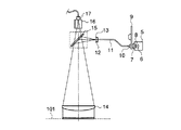
本発明の一つの実施の形態に従った欠陥検査装置について図1乃至図8を用いて説明する。図1は、本実施の形態に従った欠陥検査装置1を示す概略的な側面図である。図2は、図1中の欠陥検査装置1の波長選択部を示す概略的な側面図である。図3は、図1中の欠陥検査装置1の制御系を示す概略的なブロック図である。なお、本実施の形態の欠陥検査装置1は、多層の基板である被検体101を検査する。なお、被検体101は、最上層に、複数の周期パターンを有するレジスト層が形成されている。
A defect inspection apparatus according to an embodiment of the present invention will be described with reference to FIGS. FIG. 1 is a schematic side view showing a
欠陥検査装置1は、ステージ2と、照明部3と、結像部4と、撮像部70と、制御系200とを具備している。
ステージ2は、被検体101を保持並びに移動させる支持機構である。本実施の形態において、ステージ2は被検体101を吸着保持して互いに直交する所定の2つの軸線に沿って移動させ得るように構成されている。なお、本明細書中において、一方の軸線をX軸とし、他方の軸線をY軸とする。また、本明細書中において、X並びにY軸と直交する軸線をZ軸とする。従って、Z軸は、ステージ2に支持された被検体101の表面の法線方向と実質的に一致する。
The
The stage 2 is a support mechanism that holds and moves the subject 101. In the present embodiment, the stage 2 is configured so that the subject 101 can be adsorbed and held and moved along two predetermined axes orthogonal to each other. In this specification, one axis is defined as the X axis, and the other axis is defined as the Y axis. In the present specification, an axis perpendicular to the X and Y axes is taken as a Z axis. Accordingly, the Z axis substantially coincides with the normal direction of the surface of the subject 101 supported by the stage 2.
また、本欠陥検出装置は、検査対象となる半導体ウエハ基板かFPD用ガラス基板をステージ2上に搬送する基板搬送ロボットを備えた図示しない被検体搬送部が並設されている。この被検体搬送部には、検査前の被検体101を格納しているストッカ(カセット)と、検査後の被検体101を格納するストッカ(カセット)とを有している。 In addition, the defect detection apparatus is provided with a not-shown subject transport unit provided with a substrate transport robot that transports a semiconductor wafer substrate or FPD glass substrate to be inspected onto the stage 2. The subject transport unit includes a stocker (cassette) that stores the subject 101 before the examination and a stocker (cassette) that contains the subject 101 after the examination.
照明部3は、被検体101を照明する照明手段であり、光源31と、波長選択部32と、光ファイバー33と、コリメートレンズ34とを有している。光源31は、公知の照明装置である。本実施の形態においては、光源31は、ハロゲンランプであり、白色光を出力する。この光源31から光は、波長選択部32に入射する。具体的には、光源31からの光は、後述する波長選択部32の入射スリット32aに入射する。
The
波長選択部32は、例えば、入射スリット32aと出射スリット32aの開口の幅を変えることにより、透過波長幅が可変なモノクロメータである。この波長選択部32は、入射スリット32aと、凹面回折格子32bと、出射スリット32cとを有している。入射スリット32a並びに凹面回折格子32bは、入射スリット32aを通過した光束が凹面回折格子32bに入射するように、互いの配置が設定されている。この凹面回折格子32bは、図示しない可動装置によって図示する矢印方向に回動可能に構成されており、凹面回折格子33bを回動により出射スリット32cに入射する光の中心波長を選択可能である。
The
光ファイバー33は、出射スリット32cからの光を入射端33aから入射し、入射した光を出射端33bから出射する。出射端33bは、コリメートレンズ34の焦点上に配置されている。コリメートレンズ34は、自身を通過した光を線状の平行光に成形する。このコリメートレンズ34は、光軸と交差する被検体101の方向に沿った線状の領域を照明する。言い換えると、コリメートレンズ34は、幅方向がY軸と平行になるように配置されている。
The optical fiber 33 enters the light from the exit slit 32c from the
この照明部3は、コリメートレンズ34の光軸と被検体101の被検査面の法線(Z軸)とのなす角度(入射角度)θiが変更可能なように、図示しない回転機構を有する支持部により光ファイバー33の出射端33bが支持されている。
The illuminating
前記構成の照明部3は、コリメートレンズ34を透過し線状の光を被検体101に対して照明する。本明細書中において、この照明部3により照明する領域を、照明領域とする。照明部3の照明領域は、結像部4に結像されて、撮像部70により撮像される。
The
この結像部4は、コリメートレンズ41と、結像レンズ43とを具備している。コリメートレンズ41と結像レンズ43と後述する撮像ユニット切替部73は、コリメートレンズ41の光軸と被検体101の法線(Z軸)とのなす角度(検査角度)θdが変更可能なように、図示しない回転機構を有する支持部により支持されている。コリメートレンズ41は、前記照明領域から発生した反射光のうち、検査角度θdの反射光を集光し、結像レンズ43に導く。なお、本明細書中において、文言「反射光」とは、正反射光、回折光、並びに散乱光を含むものとする。
The imaging unit 4 includes a
結像レンズ43は、入射瞳がコリメートレンズ41の略焦点位置に配置されるように、配置が設定されている。また、結像レンズ43は、コリメートレンズ41からの光束を、対応する撮像部70上に結像させる。
The
撮像部70は、公知の撮像装置である撮像ユニット71と、入射した光を分光するとともに各波長の分光強度を測定するポリクロメータ72と、撮像ユニット切替部73とを有している。
The
撮像ユニット71は、結像レンズ43による像を撮像する撮像面71a(図4参照)を有している。本実施の形態において、撮像ユニット71は、ラインイメージセンサであり、被検体の幅全体に渡る画像を一度に撮像し得る。撮像ユニット71は、撮像ユニット切替部73により図示する矢印d2方向に移動可能に支持されている。
The
ポリクロメータ72は、受光した光を分光するとともに、その分光強度を一括して測定する分光強度測定手段である。このポリクロメータ72は、可動固定部72aと、光ファイバー72bと、ポリクロメータ本体72cとを有している。可動固定部72aは、Y軸に沿って光ファイバー72bの入射端72dを図示する矢印d1方向に移動可能に支持している。また、この可動固定部72aは、撮像ユニット切替部73により図示する矢印d2方向に移動可能に支持されている。光ファイバー72bは、出射端がポリクロメータ本体72cに接続されており、入射端72dから入射した光を、ポリクロメータ本体72cに送る。ポリクロメータ本体72cは、入射した光の分光強度を測定し、制御系200に測定結果を送る。
The
撮像ユニット切替部73は、撮像ユニット71並びに可動固定部72aを駆動する図示しない駆動部を有している。撮像ユニット切替部73は、駆動部により、撮像ユニット71並びに可動固定部72aを長手方向d1と直交する駆動方向d2に沿って移動させる。この構成により、この撮像ユニット切替部73は、制御系200の命令に従った駆動部の駆動により、撮像ユニット71並びに可動固定部72aの一方が結像レンズ43による被検体の結像位置に配置されるように、これらを選択的に移動させる。具体的には、撮像ユニット切替部73は、撮像ユニット71による撮像を行う際には、前記駆動部を制御して撮像ユニット71の撮像面71aが図4に示す結像レンズ43による像80の位置に一致するように撮像ユニット71を移動させる。このとき、ポリクロメータ72は、駆動方向d2において、像80からずれた位置に配置される。そして、前記撮像時からポリクロメータ72による測定に切り替える際には、撮像ユニット切替部73の前記駆動部を制御してポリクロメータ72の入射端72dが図5に示す像80の位置に一致するように可動固定部72aを移動させる。この際には、撮像面71aは、駆動方向d2において、像80からずれた位置に配置される。さらに、撮像ユニット切替部73は駆動部を制御し、入射端72dが長手方向d1に沿って、所望の測定位置に移動させるとともに、移動後の位置を維持するように停止させる。
The imaging
なお、撮像ユニット切替部73とポリクロメータ本体72cは、制御系200と接続されており、駆動が制御されるとともに、撮像した画像と測定結果を制御系200へ送る。 前記構成により欠陥検査装置1は、照明側の入射角度θ1と撮像側の検査角度θdを回動させる構成とすることで、照明部3により任意の入射角度θiで被検体101を照明するとともに撮像部70により任意の検査角度θdで前記照明領域からの反射光を受光し得る。
Note that the imaging
続いて、制御系200について、図3を参照して説明する。
制御系200は、ステージ制御部201と、駆動回路202と、光学系制御部203と、被検体搬送制御部204と、画像インターフェース(画像I/F)205と、画像処理装置206と、モニタ207,210と、画像記憶装置208と、ホストコンピュータ209と、キーボード211と、シーケンサ213とを有している。
Next, the
The
ステージ制御部201は、ステージ2と接続されており、ステージ2の駆動を制御する。
駆動回路202は、撮像部70に接続されており、ステージ制御部201の制御と同期して撮像部70の駆動を制御する。
The stage control unit 201 is connected to the stage 2 and controls the driving of the stage 2.
The
光学系制御部203は、照明部3並びに結像部4と接続されており、これらの駆動を制御する。より具体的には、光学系制御部203は、照明部3の照明光の光量、波長幅、並びにに中心波長を制御するとともに、照明部3並びに結像部4の被検体に対する角度(入射角度θi並びに検査角度θd)を制御する。
The optical system control unit 203 is connected to the
被検体搬送制御部204は、前述の被検体搬送部と接続されており、被検体搬送部の駆動を制御する。
画像インターフェース(画像I/F)205は、撮像部70並びに画像処理装置206と接続されている。撮像部70により取得された画像は、この画像I/F205を介して、画像処理装置206に転送される。
The subject transport control unit 204 is connected to the above-described subject transport unit, and controls the driving of the subject transport unit.
An image interface (image I / F) 205 is connected to the
画像処理装置206は、ホストコンピュータ209と接続されており、ホストコンピュータ209により駆動が制御される。この画像処理装置206は、ラインイメージセンサである撮像部70から送られてくる1ラインづつの画像を再構成し、被検体101の全体画像を作成する。さらに、画像処理装置206は、前記全体画像を画像処理し、欠陥を抽出する。また、画像処理装置206は、抽出した欠陥に関する欠陥の種類、数、位置、面積等の欠陥データをホストコンピュータ209に送る。この画像処理装置206には、さらに、モニタ207と画像記憶装置208とが接続されている。モニタ207は、画像処理装置206により作成された画像等を表示する画像表示装置である。
The
画像記憶装置208は、前記画像処理装置206で画像処理された検査画像や処理画像を格納するデータ格納装置で、被検体101と検査画像、抽出された欠陥画像、欠陥の無い良品の被検体101を撮像した参照画像などが格納されている。
The
ホストコンピュータ209は、撮像部70,画像処理装置206、モニタ210、キーボード211、及びシーケンサ213と接続されている。ホストコンピュータ209は、画像処理装置206並びにシーケンサ213の駆動を制御し、この制御のための必要な設定を、モニタ210に制御メニューとして表示する。また、ホストコンピュータ209は、ポリクロメータ72の測定結果を取得する。
The
キーボード211は、前記制御メニュー及び/又はその他の制御に必要な命令並びに情報を、ホストコンピュータ209に対して入力するための入力装置である。
シーケンサ213は、ステージ制御部201、駆動回路202、光学系制御部203、及び、被検体搬送制御部204に接続されており、これらが制御する制御対象の駆動シーケンスを、これらに送る。また、シーケンサ213は、ホストコンピュータ209からの駆動命令を、これらに送る。
The
The
なお、ホストコンピュータ209は、図示しない記憶部を有しており、この記憶部には、前記制御に必要な制御情報が格納される。前記制御情報とは、例えば、被検体の種類毎の検査条件(光学系の設定、検査面積、画像処理条件、欠陥の良否判定を行う際の合格基準など)、検査データなどである。この制御情報は、検査前に予め前記記憶部に格納しておくことも可能であるし、検査時にキーボード211等により入力し、前記記憶部に格納することも可能である。
The
以下に、前記構成の欠陥検査装置1の動作について説明する。
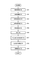
欠陥検査装置1が被検体101の検査を行う際に、まず、検査条件(レシピ)を設定する検査条件設定処理を行う。この検査条件設定処理では、被検体101の一部(例えば1ライン又は複数ライン)を撮像し、その撮像した画像に基づいて、検査時に設定する光源31の中心波長、波長幅、並びに照明部3の入射角度θi、検査角度θdを算出する。この検査条件設定処理において、本実施の形態の欠陥検査装置1は、図6に示す手順で検査条件の設定を行う。なお、ホストコンピュータ209は、検査条件設定処理を行う際の処理手順を前記記憶部に有しており、この処理手順に従って、前記検査条件を自動的に算出する。以下に図6を用いて検査条件の設定理由について説明する。
Below, operation | movement of the
When the
[被検体配置工程501]
この被検体配置工程501では、ホストコンピュータ209は、シーケンサ213を介して、被検体搬送制御部204並びにステージ制御部201に対して駆動命令を出す。この駆動命令を受けた被検体搬送制御部204は、前記被検体搬送部を駆動し、前記ストッカから被検体101を1枚取り出し、ステージ2上に配置する。続いて、被検体撮像工程502が行なわれる。なお、本実施の形態において、被検体101は、欠陥を有している検査対象の基板である。
[Subject placement step 501]
In the
[被検体撮像工程502]
この被検体撮像工程502では、ホストコンピュータ209が駆動回路202に駆動命令を出し、撮像ユニット切替部73を駆動させ、撮像ユニット71を結像位置に配置する。これとともに、ホストコンピュータ209は、光学系制御部203に駆動命令を出し、入射角度θiと検査角度θdとが一致するように、照明部3と結像部4との配置を設定する。また、ホストコンピュータ209は、この工程においての撮像時に用いられる光源の波長並びに入射角度θiを設定する。なお、この被検体撮像工程では、被検体のパターンの配置を確認することを目的として、被検体全体を撮像するため、光源の波長並びに入射角度は予め設定された基準値を設定すればよい。
[Subject imaging step 502]
In the
続いて、ホストコンピュータ209は、ステージ2をX軸に沿って駆動させ、被検体を自身の長手方向に沿って移動させる。ホストコンピュータ209は、これと同期して、撮像ユニット71に、被検体の幅方向に沿った1ラインづつ被検体101を撮像させる。また、ホストコンピュータ209は、撮像した画像を、順次画像I/F205を介して、画像処理装置206に送る。前記撮像ユニット71並びにステージ2の駆動により、被検体101の全面の撮像が完了すると、画像処理装置206は、被検体101全体を撮像した被検体全体画像を形成し、この被検体全体画像をホストコンピュータ209に送る。続いて、基準位置設定工程503が行われる。
Subsequently, the
[基準位置設定工程503]
この基準位置設定工程503では、ホストコンピュータ209が適切な中心波長並びに入射角度θiの選定を行う際に、被検体の測定箇所である基準位置を設定する。この設定時にホストコンピュータ209は、被検体全体画像を参照し被検体101上の複数のパターンの中から検査領域、例えば比較的面積の大きいパターンが形成されている位置を検出する。そして、ホストコンピュータ209は、検出したパターンにおいて欠陥の無い位置を基準位置に設定する。なお、比較的面積の大きいパターンは、被検体において重要であるため、このパターンを検査位置に設定することは好ましい。しかしながら、被検体101上において、他の位置を基準位置に設定することも可能である。
[Reference position setting step 503]
In this reference
この基準位置は、被検体全体画像を画像処理することにより検出した欠陥の無い位置に設定することも可能であるし、モニタ207に映し出された前記大きいパターンを見て、操作者が設定することも可能である。続いて、基準位置移動工程504が行われる。
This reference position can be set to a position free of defects detected by performing image processing on the entire subject image, and can be set by the operator by looking at the large pattern displayed on the
[基準位置移動工程504]
この基準位置移動工程504では、ホストコンピュータ209が、ステージ制御部201に駆動命令を出し、基準位置移動工程503で設定した基準位置が撮像ユニット71により撮像される位置に配置されるようにステージ2を移動させる。つまり、ステージ2は、前記基準位置が前記照明領域中に配置されるように、被検体101を移動させる。続いて、撮像ユニット切替部73が、入射端72dが像80の領域中に配置されるように、可動固定部72aを駆動方向d2に沿って移動させる。可動固定部72aの移動完了の後、入射端72dが、長手方向d1に沿って移動され、基準位置が結像する位置に配置される。続いて、反射率測定工程505が行われる。
[Reference position moving step 504]
In the reference
[反射率測定工程505]
この反射率測定工程505では、ホストコンピュータ209が、光学系制御部203に駆動命令を出し、光源31からの白色光を光ファイバー33に入射するように、波長選択部32を設定する。この設定は、凹面回折格子32bを、入射スリット32aからの光束が出射スリット32cに収束するように正反射させる角度に回動させることにより達成される。続いて、入射角度θiと検査角度θdとを一致させた状態のまま、小さい角度から大きい角度に移動させる。この移動に伴って、ポリクロメータ72が、前記基準位置の分光反射強度を測定し、その測定結果である反射率データをホストコンピュータ209に取り込む。この測定により、各入射角毎に、所定の幅の波長においての各波長に対応した反射率が求まる。
[Reflectance measurement step 505]
In this
なお、前記反射率データには、光源31の分光強度、ポリクロメータ72の分光感度、及びこれらの間の各光学素子の分光反射率又は透過率が反映されてしまっている。このため、続く補正工程506において、上述の反射率データを補正する。
The reflectance data reflects the spectral intensity of the light source 31, the spectral sensitivity of the
[補正工程506]
補正工程506では、ホストコンピュータ209が、予め用意してある各波長及び入射角度θi毎の補正係数を前記記憶部から取り出し、前記反射率データの各波長及び入射角毎に対応した前記反射率に乗じて、前記反射率データを補正する。この補正係数は、以下のようにして、求められ、前記記憶部中に格納される。この補正係数を求めるために、分光屈折率が既知である平面板(例えば単結晶シリコンなど)を準備し、この平面板の反射率データを反射率測定工程505と同様な手順で測定し、各波長及び入射角度θiにおける反射率を分光屈折率から計算する。これらの各波長及び入射角における反射率の計算値を測定データで割ることにより、各波長及び入射角度θi毎の補正係数が得られる。このように反射率測定工程505により測定された反射率データの補正後、続いて、中心波長入射角度設定工程507が行われる。
[Correction process 506]
In the
[中心波長入射角度設定工程507]
中心波長入射角度設定工程507では、補正工程506により補正後の反射率データから、検査条件のうちの中心波長と入射角度θiとを求め、検査条件として設定する。
[Center wavelength incident angle setting step 507]
In the center wavelength incident
なお、欠陥を検出する際に、被検体の欠陥は、欠陥の有していない(正常な)被検体を撮像した参照画像と、被検体101を撮像した被検体全体の画像である検査画像とを比較し、これらの輝度値の変化により、検出される。従って、より確実に欠陥を検出するためには、欠陥と、欠陥の有していない部位とが、大きい輝度差になることが好ましい。このため、前記中心波長と、入射角度θiとは、検査対象の欠陥と、被検体上の正常な部位とを比較した際に、明確に輝度差が現れ得る値を選定する。このような中心波長並びに入射角度θiを求めるために、中心波長入射角度設定工程507は、以下のようにして行われる。
Note that when detecting a defect, the defect of the subject includes a reference image obtained by imaging a (normal) subject having no defect, and an inspection image that is an image of the entire subject obtained by imaging the subject 101. Are detected by the change of these luminance values. Therefore, in order to detect a defect more reliably, it is preferable that the defect and the portion having no defect have a large luminance difference. For this reason, the central wavelength and the incident angle θi are selected such that a luminance difference can clearly appear when comparing the defect to be inspected with a normal part on the subject. In order to obtain such a center wavelength and incident angle θi, the center wavelength incident
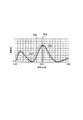
まず、前記補正後の反射率データより、前記基準位置における反射率の分布を調べる。なお、この基準位置は、前述のように、被検体101の欠陥の有していない正常な部位である。従って、これにより、正常な部位の反射率の分布を調べ得る。この分布は、図7中のように示される。この図7中において、各波長並びに入射角度θiの反射率は、凡例602に示されるようにグレースケールに変換され、横軸を波長、縦軸を入射角度θiに設定し、2次元的に分布させて示されている。この反射率データの分布により、入射角度並びに波長に対応する前記基準位置の反射率特性の関数(反射率データに基づく関数)が求められ得る。この凡例において、白で塗られた領域は、前記反射率データに基づく関数の極大値の位置を示している。
First, the reflectance distribution at the reference position is examined from the corrected reflectance data. Note that this reference position is a normal part having no defect of the subject 101 as described above. Therefore, the reflectance distribution of the normal part can be examined by this. This distribution is shown in FIG. In FIG. 7, the reflectance of each wavelength and the incident angle θi is converted to gray scale as shown in the
一般的に、図7中に示されるような被検体101の反射率の分布は、被検体の種類及び撮像位置によって複雑に変化する。また、欠陥の反射率データは、正常な部位の反射率データと比較した場合、欠陥の種類により、複雑に変化する。このような複雑な変化を示す反射率データであるが、代表的な欠陥においての反射率は、正常な被検体の表面の反射率に対して、ある程度決まった変化をする。例えば、レジストの周期パターンの線幅が所定の幅より狭くなってしまった欠陥(線幅欠陥)では、前記分布において、分光反射率における反射率の極大値の値と、その極大値の位置とがシフトする。このことは、膜厚むらのような欠陥においても同様である。従って、欠陥と、正常な部位との反射率の差は、正常な部位の反射率データの前記極大値における入射角度θi並びに波長において比べることにより、差が出やすい。 In general, the reflectance distribution of the subject 101 as shown in FIG. 7 changes in a complicated manner depending on the type of the subject and the imaging position. Further, the defect reflectance data changes in a complicated manner depending on the type of defect when compared with the reflectance data of a normal part. Although the reflectance data shows such a complicated change, the reflectance at a typical defect changes to some extent with respect to the reflectance of the surface of a normal subject. For example, in the defect (line width defect) in which the line width of the periodic pattern of the resist is narrower than a predetermined width, in the distribution, the value of the maximum value of the reflectance in the spectral reflectance and the position of the maximum value Shifts. This also applies to defects such as film thickness unevenness. Therefore, the difference in reflectance between the defect and the normal part can be easily made by comparing the incident angle θi and the wavelength at the maximum value of the reflectance data of the normal part.
また、前記反射率データにおいて、入射角度θiを決定した場合、この入射角度θiにおいての反射率の分布は、波長の値順に結ぶことにより、曲線のグラフ(反射率曲線)として示され得る。例えば、図7中の参照符号603で指摘された極大値の領域の前記反射率曲線は、入射角度θiが60度に設定されている際の各反射率を、波長の値順にプロットすることにより形成される。このようにして作成された入射角度60度における反射率曲線が、図8中において、参照符号702で指摘されている。反射率曲線703は、正常な部位(基準位置)においての反射率曲線である。この図8中に、前記線幅欠陥の反射率データにおいての入射角度60度の反射率曲線703が、破線により示されている。両者を比較した場合においても、前記欠陥の反射率曲線703は、正常な部位の反射率曲線702に対して、極大値のピークの高さと、位置とが変化している。具体的には、反射率曲線702のピーク波長で、反射率曲線702と、反射率曲線703とを比較すると、これらの差を、反射率の差として検出し得る。なお、反射率曲線703と反射率曲線702との交点の波長705でこれらを比較した場合、反射率の差が出ない。従って、波長の選定によっては、正常な被検体と欠陥の有る被検体とを比較出来ないことが分かる。これらにより、欠陥の反射率データは、正常な部位の反射率データにおいての反射率の極大値と、比較することにより、ピークの差が明確になる可能性が大きく、有用であることが分かる。なお、前記欠陥の反射率データは、測定したい欠陥に対して、反射率測定工程505並びに補正工程506を行うことで測定可能である。
Further, when the incident angle θi is determined in the reflectance data, the reflectance distribution at the incident angle θi can be shown as a curve graph (reflectance curve) by connecting them in order of wavelength values. For example, the reflectance curve in the region of the maximum value pointed out by
本工程において、具体的には前記極大値は、入射角度θi並びに波長の測定レンジにおいての両端が誤差を含んでいる可能性があるため、これらを除き、それ以外のものから選定される。ホストコンピュータ209は、上述のようにして選定した極大値における入射角度θi並びに波長を、検査時においての正反射光撮像においての検査条件(入射角度θiと中心波長)として、記憶する。このように、本実施の形態のホストコンピュータ209は、反射率データに基づいて、前記欠陥の検出に用いる画像の撮像時(検査時)の前記中心波長と、入射角度θiとを設定する検査条件設定部である。続いて、波長幅可変撮像工程508が行われる。
In this step, specifically, the maximum value is selected from other than that except for the incident angle θi and the both ends in the wavelength measurement range, which may contain errors. The
[波長幅可変撮像工程508]
この波長幅可変撮像工程508では、まず、ホストコンピュータ209は、波長選択部32の選択する波長を、中心波長入射角度設定工程507により求めた中心波長に設定する。これとともに、照明部3も同様に、中心波長入射角度設定工程507で求めた入射角度θiに、設定する。これに対応して、結像部4の検査角度θdも設定する。また、撮像部70は、撮像ユニット71により撮像し得るように、撮像ユニット切替部73を設定する。
[Variable wavelength imaging process 508]
In the variable wavelength
この状態で、波長選択部32が、波長幅を最小にして、被検体101の全面を撮像する。撮像を終えた後、波長幅を順に大きくしていき、所定の最大幅まで、被検体101の全面の撮影を繰り返す。撮像した各画像は、ホストコンピュータ209に保存される。なお、撮像する波長幅の最小幅並びに最大幅、及び、撮影後の波長幅の増分は、ホストコンピュータ209中に予め格納していてもよいし、操作者によりキーボードを介して入力させることも可能である。続いて、波長幅設定工程509が行われる。
In this state, the
[波長幅設定工程509]
この波長幅設定工程では、波長幅可変撮像工程508で撮像された各画像が、モニタ207に表示される。使用者が、前記表示画像から、膜厚むらなどの、レジスト層より下層の欠陥の影響が十分に抑制された画像の中から、最小の波長幅で撮像された画像を選択する。そして、ホストコンピュータ209は、その画像の波長幅を、記憶するとともに、波長選択部32に設定する。
このようにして、検査条件設定処理は、終了する。
[Wavelength setting step 509]
In this wavelength width setting step, each image captured in the wavelength width
In this way, the inspection condition setting process ends.
つづいて、上述のように検査条件が設定された後の欠陥検査装置1の動作について説明する。モニタ210に操作メニューが表示され、操作者がキーボード211により、被検体101の種類とともに、検査開始を指示すると、ホストコンピュータ209に格納されている検査条件の中から被検体101に該当する条件が検索される。この検索された条件が、シーケンサ213を介して光学系制御部203に伝えられ、光学系制御部203により、照明部3、結像部4、並びに撮像部70の設定が行われる。このとき、撮像ユニット切替部73は、結像部4の結像位置に、撮像ユニット71を配置する。
Next, the operation of the
続いて、ホストコンピュータ209は、図示しないストッカから検査対象の被検体101を一枚取り出し、ステージ2上に配置する。ステージ2は、一定速度で被検体101を、X軸に沿って搬送し、この搬送と同期して撮像ユニット71により被検体101を1ラインずつ撮像する。この撮像されたライン状の画像は、画像I/F205を介して画像処理装置206に送られ、被検体全体の画像である検査画像が形成される。画像処理装置206は、画像記憶装置208から参照画像を呼び出し、前記検査画像と比較し、欠陥を検出する。また、画像処理装置206は、検出した欠陥の位置、面積等のデータを、ホストコンピュータ209に送る。ホストコンピュータ209は、欠陥の数、並びに面積等を、被検体101の合格基準と照合し、良否判定を行う。検査が終了した際に、被検体101は、良否に区分けされ、図示しない検査後の被検体を格納するストッカに搬送される。このようにして、1枚の被検体101の検査を終了する。
Subsequently, the
このように、本実施の形態の欠陥検査装置1は、被検体101の正常な部位(欠陥の有していない部位)の反射率データを測定し、この反射率データに基づいて、検出対象の欠陥を検出するのに適した、照明部3の入射角度θi並びに中心波長を含む検査条件を決定し得る。これにより、本実施の形態の欠陥検査装置1は、煩雑な検査条件を容易に設定し得るとともに、前記設定の結果、確実に対象の欠陥を検出し得る。
As described above, the
また、本実施の形態の撮像ユニット71は、ラインイメージセンサである。これとともに、ステージ2は、被検体101を、前記ラインイメージセンサの撮像領域の長さ方向と、この長さ方向と略直交する方向とに、撮像ユニット71に対して相対的に移動させ得る。この構成により、本実施の形態の欠陥検査装置1は、ステージ2と撮像ユニット71とを同期させて駆動させることにより、確実に被検体の全面を撮像可能でありながら、エリアイメージセンサを有する場合に比べて、小型化が可能である。しかしながら、撮像ユニット71は、被検体101の全面を一括撮像し得るエリアイメージセンサに代えることも可能である。
The
また、本実施の形態のポリクロメータ72は、前記光源に含まれる波長帯の光を分光するとともに、その分光強度を一括測定する分光強度測定手段である。欠陥検査装置1は、この分光強度測定手段により前記反射率データを測定し得る。このため、欠陥検査装置1は、一括して所定の波長範囲の反射率データを取得することが出来、より迅速な測定を行い得る。
また、ホストコンピュータ209は、前記検査条件設定処理の処理手順に従って、前記中心波長と入射角度とを自動的に設定する。従って、本実施の形態の欠陥検査装置1は、煩雑な検査条件の設定を容易に行い得る。
The
The
また、ホストコンピュータ209は、前記の検査条件の自動設定において、反射率データの極値においての波長と入射角度θiを、検査条件の中心波長と入射角度θiに設定する。これにより、本実施の形態の欠陥検査装置1は、検査時において欠陥と、正常な部位との反射率の差が出やすい中心波長と入射角度θiを、より確実に求め、設定し得る。
In the automatic setting of the inspection condition, the
なお、本実施の形態において、例えば、欠陥と正常な部位との反射率データを比較した際に、極大値のピークと位置とのシフト量が小さい場合、極大値又は極小値の近傍の波長704では、図9に示されるように、反射率の差が顕著には出ない。このような場合には、極大値と極小値の中間にある分光反射率(波長や入射角度に対する傾き)の大きい領域を用いることが有利であり、前記反射率データに基づく関数を微分処理し、その極値の入射角度θi並びに波長を、検査時の入射角度θi並びに中心波長として設定する。このように選定すると、適切な入射角度θiと図9中において参照符号706で指摘されたような中心波長が選定される。このように選定した場合、波長704を選定した場合より、大きい反射率の差で検査し得るため、好ましい。
In the present embodiment, for example, when the reflectance data of a defect and a normal part are compared, and the shift amount between the peak of the maximum value and the position is small, the
また、本実施の形態において、撮像ユニット71は、波長選択部32と協働して複数の波長幅により、被検体101を撮像する。これらの画像は、互いに比較され、この比較結果に基づいて撮像に用いる光の波長幅が決定される。本実施の形態の欠陥検査装置1は、このような比較結果に基づいて波長幅を決定し得るため、より確実に適切な波長幅を選定し得る。
Further, in the present embodiment, the
なお、本実施の形態においては、操作者が複数の波長幅の画像を確認し得るように、これらの画像が、モニタ207に表示されるとともに、選択した画像の波長幅を、検査条件に設定し得る。従って、操作者が、好ましい検査結果を得れる画像を選定するのみで、適切な波長幅の設定を行い得る。また、画像処理装置206が、これらの画像に対して欠陥検出の画像処理を適用し、誤検出の少ない画像を選定し、この選定した画像を撮像した波長幅を、検査条件の波長幅と設定することも可能である。これにより、欠陥検査装置1は、波長幅の選定を自動で行い得る。
In the present embodiment, these images are displayed on the
また、本実施の形態において、撮像ユニット71の撮像位置と、ポリクロメータ72の測定位置とは、同一に設定されている。しかしながら、結像部4中にハーフミラー等を配置し、光路を分岐させ、分岐された光路に撮像ユニット71並びにポリクロメータ72を分配して、前記測定位置を分けることも可能である。このようにして、撮像ユニット71の撮像位置と、ポリクロメータ72の測定位置とを、別の位置に設定した場合、撮像ユニット切替部73を省略することが可能である。また、撮像ユニット71と、ポリクロメータ72とが、別々の駆動部により駆動するようにし、撮像ユニット切替部73を省略することも可能である。
In the present embodiment, the imaging position of the
また、本実施の形態において、反射率データを測定する際に、波長並びに入射角度θiの測定間隔は任意に設定され得る。さらに、これらの測定間隔を大きくし、各データの間を適切に補間することにより測定速度を短縮することが可能である。 In this embodiment, when measuring reflectance data, the wavelength and the measurement interval of the incident angle θi can be set arbitrarily. Furthermore, the measurement speed can be shortened by increasing these measurement intervals and appropriately interpolating between the data.
また、本実施の形態の波長幅可変撮像工程508は、以下の波長幅可変撮像工程508’のように、代えることも可能である。波長幅可変撮像工程508’では、波長幅可変撮像工程508と同様に、照明部と撮像部の角度θiとθdを中心波長入射角度設定工程507で設定された検査条件の角度に設定する。さらに波長選択部32の波長幅を最小に設定する。この状態で、波長選択部32が、中心波長を検査時の中心波長の近傍で変化させながら、各中心波長に対する被検体全面の画像を撮像ユニット71により撮像する。このようにして撮像した画像群を積分する。このような波長幅可変撮像工程508’を行った場合、欠陥検査装置1は、前記画像群を積分することにより、任意の波長幅に対応した画像を取得し得る。
Further, the variable wavelength
また、本実施の形態の反射率測定工程505は、以下の反射率測定工程505’のように代えることも可能である。反射率測定工程505’では、撮像ユニット切替部73を駆動させ、撮像ユニット71を、結像部4による像の結像位置に配置する。これとともに、照明部3の入射角度θiと、結像部4の検査角度θdを最小に設定する。続いて、波長選択部32は、波長幅を最小にした状態で、中心波長を最小から最大へ変化させる。これと同期して撮像ユニット(リニアイメージセンサ)71は、各中心波長毎に、被検体101の幅方向において、前記基準位置を含む1ラインの画像を撮像する。この撮像が完了した後、入射角度θi並びに検査角度θdを、一定の変化幅で変化させつつ、同様の撮像を繰り返す。すべての撮像が終了した後、基準位置を含む画素の輝度を、反射率データとしてホストコンピュータ209に取り込む。この反射率測定工程505’によれば、ポリクロメータ72を省略し得る。
Further, the
1…欠陥検査装置、101…被検体、2…ステージ、d1…長手方向、d2…駆動方向、200…制御系、201…ステージ制御部、202…駆動回路、203…光学系制御部、204…被検体搬送制御部、205…画像インターフェース、206…画像処理装置、207…モニタ、208…画像処理装置、209…ホストコンピュータ、210…モニタ、211…キーボード、213…シーケンサ、3…照明部、31…光源、32…波長選択部、32a…入射スリット、32b…凹面回折格子、32c…出射スリット、33…光ファイバー、33a…入射端、33b…他端、34…コリメートレンズ、4…結像部、41…コリメートレンズ、43…結像レンズ、501…被検体配置工程、502…被検体撮像工程、503…基準位置設定工程、504…基準位置移動工程、505…反射率測定工程、506…補正工程、507…中心波長入射角度設定工程、508…波長幅可変撮像工程、509…波長幅設定工程、602…凡例、70…撮像部、702、703…反射率曲線、71…撮像ユニット、71a…撮像面、72…ポリクロメータ、72a…可動固定部、72b…光ファイバー、72c…ポリクロメータ本体、72d…入射端、73…撮像切替部、8…熱吸収フィルタ、80…像、θd…検査角度、θi…入射角度
DESCRIPTION OF
Claims (1)
前記照明手段からの平行光束うちの前記被検体からの反射光を集光し、前記被検体の像を結像する結像手段と、
前記結像手段により結像された像を撮像する撮像手段と、
前記光源と撮像手段との間の光路中に配置され、前記光路中の光束の中心波長並びに波長幅を設定する波長選択手段と、
前記撮像手段により撮像された画像から前記被検体の欠陥を検出する欠陥検出部と、
前記照明手段の照明光の入射角度を設定する角度設定手段と、
複数の中心波長並びに入射角度で測定された前記被検体の欠陥の有していない部位の反射率データを取得し、前記反射率データに基づいて、前記欠陥の検出に用いる画像の撮像時の前記中心波長と、入射角度とを設定する検査条件設定部と、を具備する欠陥検査装置。 Illuminating means for illuminating the subject with illumination light from the light source as a substantially parallel light beam;
Imaging means for condensing the reflected light from the subject out of the parallel luminous flux from the illuminating means, and forming an image of the subject;
Imaging means for capturing an image formed by the imaging means;
A wavelength selection unit that is disposed in an optical path between the light source and the imaging unit and sets a center wavelength and a wavelength width of a light beam in the optical path;
A defect detection unit that detects a defect of the subject from an image captured by the imaging unit;
An angle setting means for setting an incident angle of illumination light of the illumination means;
Obtaining reflectance data of a portion of the subject that does not have a defect measured at a plurality of center wavelengths and incident angles, and based on the reflectance data, the image at the time of capturing an image used for detection of the defect A defect inspection apparatus comprising: an inspection condition setting unit that sets a center wavelength and an incident angle.
Priority Applications (1)
| Application Number | Priority Date | Filing Date | Title |
|---|---|---|---|
| JP2004083569A JP2005274156A (en) | 2004-03-22 | 2004-03-22 | Flaw inspection device |
Applications Claiming Priority (1)
| Application Number | Priority Date | Filing Date | Title |
|---|---|---|---|
| JP2004083569A JP2005274156A (en) | 2004-03-22 | 2004-03-22 | Flaw inspection device |
Publications (2)
| Publication Number | Publication Date |
|---|---|
| JP2005274156A true JP2005274156A (en) | 2005-10-06 |
| JP2005274156A5 JP2005274156A5 (en) | 2007-04-26 |
Family
ID=35174008
Family Applications (1)
| Application Number | Title | Priority Date | Filing Date |
|---|---|---|---|
| JP2004083569A Pending JP2005274156A (en) | 2004-03-22 | 2004-03-22 | Flaw inspection device |
Country Status (1)
| Country | Link |
|---|---|
| JP (1) | JP2005274156A (en) |
Cited By (8)
| Publication number | Priority date | Publication date | Assignee | Title |
|---|---|---|---|---|
| JP2008076827A (en) * | 2006-09-22 | 2008-04-03 | Toppan Printing Co Ltd | Method for setting illumination angle in defect inspection instrument |
| JP2008175565A (en) * | 2007-01-16 | 2008-07-31 | Fujifilm Corp | Flaw detector of light transmissive member, and flaw detection method |
| JP2009150832A (en) * | 2007-12-21 | 2009-07-09 | Hitachi Ltd | Method and device for inspecting pattern on hard disk medium |
| JP2010527008A (en) * | 2007-05-07 | 2010-08-05 | ケーエルエー−テンカー・コーポレーション | Computer-implemented method, computer-readable medium, and apparatus for identifying one or more optical modes of an inspection apparatus as candidates for use in inspecting a layer of a wafer |
| JP2011096305A (en) * | 2009-10-28 | 2011-05-12 | Hitachi High-Technologies Corp | Apparatus and method for inspecting surface defect on both sides of optical magnetic disk |
| JP2011129208A (en) * | 2009-12-18 | 2011-06-30 | Hitachi High-Technologies Corp | Device and method for inspection of hard disk surface for patterned media |
| JP2014027319A (en) * | 2013-11-06 | 2014-02-06 | Sokudo Co Ltd | Substrate processing apparatus, and inspection periphery exposure apparatus |
| KR20210143118A (en) * | 2020-05-19 | 2021-11-26 | 어플라이드 머티어리얼스, 인코포레이티드 | Image based metrology of surface deformations |
Citations (8)
| Publication number | Priority date | Publication date | Assignee | Title |
|---|---|---|---|---|
| JPS61138102A (en) * | 1984-12-11 | 1986-06-25 | Kawasaki Steel Corp | Method for measuring amount of oil coated on surface of steel plate |
| JPH01250708A (en) * | 1988-03-30 | 1989-10-05 | Dainippon Screen Mfg Co Ltd | Apparatus for detecting membrane pattern |
| JPH06118009A (en) * | 1992-10-05 | 1994-04-28 | Matsushita Electric Ind Co Ltd | Foreign matter inspecting device and method therefor |
| JPH1038772A (en) * | 1996-07-19 | 1998-02-13 | Murata Mfg Co Ltd | Measuring method for liquid sample, sample holder and x-ray diffractometer therefor |
| JPH10253546A (en) * | 1997-03-12 | 1998-09-25 | Toshiba Corp | Method and equipment for evaluating semiconductor substrate |
| JPH11264800A (en) * | 1998-03-18 | 1999-09-28 | Nikon Corp | Inspecting device |
| JP2000077494A (en) * | 1998-08-27 | 2000-03-14 | Hitachi Ltd | Manufacture of semiconductor integrated circuit device |
| WO2001071323A1 (en) * | 2000-03-24 | 2001-09-27 | Olympus Optical Co., Ltd. | Apparatus for detecting defect |
-
2004
- 2004-03-22 JP JP2004083569A patent/JP2005274156A/en active Pending
Patent Citations (8)
| Publication number | Priority date | Publication date | Assignee | Title |
|---|---|---|---|---|
| JPS61138102A (en) * | 1984-12-11 | 1986-06-25 | Kawasaki Steel Corp | Method for measuring amount of oil coated on surface of steel plate |
| JPH01250708A (en) * | 1988-03-30 | 1989-10-05 | Dainippon Screen Mfg Co Ltd | Apparatus for detecting membrane pattern |
| JPH06118009A (en) * | 1992-10-05 | 1994-04-28 | Matsushita Electric Ind Co Ltd | Foreign matter inspecting device and method therefor |
| JPH1038772A (en) * | 1996-07-19 | 1998-02-13 | Murata Mfg Co Ltd | Measuring method for liquid sample, sample holder and x-ray diffractometer therefor |
| JPH10253546A (en) * | 1997-03-12 | 1998-09-25 | Toshiba Corp | Method and equipment for evaluating semiconductor substrate |
| JPH11264800A (en) * | 1998-03-18 | 1999-09-28 | Nikon Corp | Inspecting device |
| JP2000077494A (en) * | 1998-08-27 | 2000-03-14 | Hitachi Ltd | Manufacture of semiconductor integrated circuit device |
| WO2001071323A1 (en) * | 2000-03-24 | 2001-09-27 | Olympus Optical Co., Ltd. | Apparatus for detecting defect |
Cited By (9)
| Publication number | Priority date | Publication date | Assignee | Title |
|---|---|---|---|---|
| JP2008076827A (en) * | 2006-09-22 | 2008-04-03 | Toppan Printing Co Ltd | Method for setting illumination angle in defect inspection instrument |
| JP2008175565A (en) * | 2007-01-16 | 2008-07-31 | Fujifilm Corp | Flaw detector of light transmissive member, and flaw detection method |
| JP2010527008A (en) * | 2007-05-07 | 2010-08-05 | ケーエルエー−テンカー・コーポレーション | Computer-implemented method, computer-readable medium, and apparatus for identifying one or more optical modes of an inspection apparatus as candidates for use in inspecting a layer of a wafer |
| JP2009150832A (en) * | 2007-12-21 | 2009-07-09 | Hitachi Ltd | Method and device for inspecting pattern on hard disk medium |
| JP2011096305A (en) * | 2009-10-28 | 2011-05-12 | Hitachi High-Technologies Corp | Apparatus and method for inspecting surface defect on both sides of optical magnetic disk |
| JP2011129208A (en) * | 2009-12-18 | 2011-06-30 | Hitachi High-Technologies Corp | Device and method for inspection of hard disk surface for patterned media |
| JP2014027319A (en) * | 2013-11-06 | 2014-02-06 | Sokudo Co Ltd | Substrate processing apparatus, and inspection periphery exposure apparatus |
| KR20210143118A (en) * | 2020-05-19 | 2021-11-26 | 어플라이드 머티어리얼스, 인코포레이티드 | Image based metrology of surface deformations |
| KR102687194B1 (en) | 2020-05-19 | 2024-07-19 | 어플라이드 머티어리얼스, 인코포레이티드 | Image based metrology of surface deformations |
Similar Documents
| Publication | Publication Date | Title |
|---|---|---|
| US7372062B2 (en) | Defect inspection device and substrate manufacturing system using the same | |
| KR101656045B1 (en) | System and method for inspecting a wafer | |
| KR100795286B1 (en) | Apparatus for detecting defect | |
| KR101793584B1 (en) | Inspecting apparatus and inspecting method | |
| US8411264B2 (en) | Method and apparatus for inspecting defects | |
| JPWO2006126596A1 (en) | Surface defect inspection equipment | |
| JP2006005360A (en) | Method and system for inspecting wafer | |
| KR100403188B1 (en) | Defect testing apparatus | |
| KR100411356B1 (en) | Apparatus for inspecting surface | |
| JP4632564B2 (en) | Surface defect inspection equipment | |
| WO2009133849A1 (en) | Inspection device | |
| JP2008128811A (en) | Defect inspection device | |
| US6735333B1 (en) | Pattern inspection apparatus | |
| JP2011174764A (en) | Inspecting method and inspecting device | |
| JP2005274156A (en) | Flaw inspection device | |
| JP2008175818A (en) | Surface inspection apparatus and method | |
| JP2003021787A (en) | Observation device | |
| JP4622933B2 (en) | Surface inspection method and surface inspection apparatus | |
| JP4162319B2 (en) | Defect inspection equipment | |
| JP3078784B2 (en) | Defect inspection equipment | |
| JPH10213552A (en) | Surface fault inspection method | |
| JPH10206337A (en) | Automatic visual inspection device for semiconductor wafer | |
| JP2000028535A (en) | Defect inspecting device | |
| JP2011141136A (en) | Inspection apparatus | |
| JP2005274161A (en) | Flaw inspection device |
Legal Events
| Date | Code | Title | Description |
|---|---|---|---|
| A521 | Written amendment |
Free format text: JAPANESE INTERMEDIATE CODE: A523 Effective date: 20070313 |
|
| A621 | Written request for application examination |
Effective date: 20070313 Free format text: JAPANESE INTERMEDIATE CODE: A621 |
|
| A977 | Report on retrieval |
Free format text: JAPANESE INTERMEDIATE CODE: A971007 Effective date: 20090918 |
|
| A131 | Notification of reasons for refusal |
Free format text: JAPANESE INTERMEDIATE CODE: A131 Effective date: 20091027 |
|
| A521 | Written amendment |
Free format text: JAPANESE INTERMEDIATE CODE: A523 Effective date: 20091222 |
|
| A02 | Decision of refusal |
Effective date: 20100601 Free format text: JAPANESE INTERMEDIATE CODE: A02 |