JP2005259739A - Substrate - Google Patents
Substrate Download PDFInfo
- Publication number
- JP2005259739A JP2005259739A JP2004065100A JP2004065100A JP2005259739A JP 2005259739 A JP2005259739 A JP 2005259739A JP 2004065100 A JP2004065100 A JP 2004065100A JP 2004065100 A JP2004065100 A JP 2004065100A JP 2005259739 A JP2005259739 A JP 2005259739A
- Authority
- JP
- Japan
- Prior art keywords
- circuit board
- flux
- electronic components
- terminals
- soldering
- Prior art date
- Legal status (The legal status is an assumption and is not a legal conclusion. Google has not performed a legal analysis and makes no representation as to the accuracy of the status listed.)
- Withdrawn
Links
Images


Classifications
-
- H—ELECTRICITY
- H05—ELECTRIC TECHNIQUES NOT OTHERWISE PROVIDED FOR
- H05K—PRINTED CIRCUITS; CASINGS OR CONSTRUCTIONAL DETAILS OF ELECTRIC APPARATUS; MANUFACTURE OF ASSEMBLAGES OF ELECTRICAL COMPONENTS
- H05K1/00—Printed circuits
- H05K1/02—Details
- H05K1/0272—Adaptations for fluid transport, e.g. channels, holes
-
- H—ELECTRICITY
- H05—ELECTRIC TECHNIQUES NOT OTHERWISE PROVIDED FOR
- H05K—PRINTED CIRCUITS; CASINGS OR CONSTRUCTIONAL DETAILS OF ELECTRIC APPARATUS; MANUFACTURE OF ASSEMBLAGES OF ELECTRICAL COMPONENTS
- H05K3/00—Apparatus or processes for manufacturing printed circuits
- H05K3/30—Assembling printed circuits with electric components, e.g. with resistor
- H05K3/32—Assembling printed circuits with electric components, e.g. with resistor electrically connecting electric components or wires to printed circuits
- H05K3/34—Assembling printed circuits with electric components, e.g. with resistor electrically connecting electric components or wires to printed circuits by soldering
- H05K3/341—Surface mounted components
-
- H—ELECTRICITY
- H05—ELECTRIC TECHNIQUES NOT OTHERWISE PROVIDED FOR
- H05K—PRINTED CIRCUITS; CASINGS OR CONSTRUCTIONAL DETAILS OF ELECTRIC APPARATUS; MANUFACTURE OF ASSEMBLAGES OF ELECTRICAL COMPONENTS
- H05K1/00—Printed circuits
- H05K1/18—Printed circuits structurally associated with non-printed electric components
- H05K1/181—Printed circuits structurally associated with non-printed electric components associated with surface mounted components
-
- H—ELECTRICITY
- H05—ELECTRIC TECHNIQUES NOT OTHERWISE PROVIDED FOR
- H05K—PRINTED CIRCUITS; CASINGS OR CONSTRUCTIONAL DETAILS OF ELECTRIC APPARATUS; MANUFACTURE OF ASSEMBLAGES OF ELECTRICAL COMPONENTS
- H05K2201/00—Indexing scheme relating to printed circuits covered by H05K1/00
- H05K2201/09—Shape and layout
- H05K2201/09009—Substrate related
- H05K2201/09063—Holes or slots in insulating substrate not used for electrical connections
-
- H—ELECTRICITY
- H05—ELECTRIC TECHNIQUES NOT OTHERWISE PROVIDED FOR
- H05K—PRINTED CIRCUITS; CASINGS OR CONSTRUCTIONAL DETAILS OF ELECTRIC APPARATUS; MANUFACTURE OF ASSEMBLAGES OF ELECTRICAL COMPONENTS
- H05K2201/00—Indexing scheme relating to printed circuits covered by H05K1/00
- H05K2201/10—Details of components or other objects attached to or integrated in a printed circuit board
- H05K2201/10007—Types of components
- H05K2201/10053—Switch
-
- H—ELECTRICITY
- H05—ELECTRIC TECHNIQUES NOT OTHERWISE PROVIDED FOR
- H05K—PRINTED CIRCUITS; CASINGS OR CONSTRUCTIONAL DETAILS OF ELECTRIC APPARATUS; MANUFACTURE OF ASSEMBLAGES OF ELECTRICAL COMPONENTS
- H05K2201/00—Indexing scheme relating to printed circuits covered by H05K1/00
- H05K2201/10—Details of components or other objects attached to or integrated in a printed circuit board
- H05K2201/10431—Details of mounted components
- H05K2201/10507—Involving several components
- H05K2201/10522—Adjacent components
-
- H—ELECTRICITY
- H05—ELECTRIC TECHNIQUES NOT OTHERWISE PROVIDED FOR
- H05K—PRINTED CIRCUITS; CASINGS OR CONSTRUCTIONAL DETAILS OF ELECTRIC APPARATUS; MANUFACTURE OF ASSEMBLAGES OF ELECTRICAL COMPONENTS
- H05K2203/00—Indexing scheme relating to apparatus or processes for manufacturing printed circuits covered by H05K3/00
- H05K2203/11—Treatments characterised by their effect, e.g. heating, cooling, roughening
- H05K2203/1178—Means for venting or for letting gases escape
-
- H—ELECTRICITY
- H05—ELECTRIC TECHNIQUES NOT OTHERWISE PROVIDED FOR
- H05K—PRINTED CIRCUITS; CASINGS OR CONSTRUCTIONAL DETAILS OF ELECTRIC APPARATUS; MANUFACTURE OF ASSEMBLAGES OF ELECTRICAL COMPONENTS
- H05K2203/00—Indexing scheme relating to apparatus or processes for manufacturing printed circuits covered by H05K3/00
- H05K2203/30—Details of processes not otherwise provided for in H05K2203/01 - H05K2203/17
- H05K2203/304—Protecting a component during manufacturing
-
- Y—GENERAL TAGGING OF NEW TECHNOLOGICAL DEVELOPMENTS; GENERAL TAGGING OF CROSS-SECTIONAL TECHNOLOGIES SPANNING OVER SEVERAL SECTIONS OF THE IPC; TECHNICAL SUBJECTS COVERED BY FORMER USPC CROSS-REFERENCE ART COLLECTIONS [XRACs] AND DIGESTS
- Y02—TECHNOLOGIES OR APPLICATIONS FOR MITIGATION OR ADAPTATION AGAINST CLIMATE CHANGE
- Y02P—CLIMATE CHANGE MITIGATION TECHNOLOGIES IN THE PRODUCTION OR PROCESSING OF GOODS
- Y02P70/00—Climate change mitigation technologies in the production process for final industrial or consumer products
- Y02P70/50—Manufacturing or production processes characterised by the final manufactured product
Abstract
Description
本発明は、電子部品の端子を半田付けするためのランドパターンを有する回路基板、特に、半田付け時に発生するフラックス等による電子部品の悪影響を防止するようにした回路基板に関する。 The present invention relates to a circuit board having a land pattern for soldering terminals of an electronic component, and more particularly to a circuit board configured to prevent an electronic component from being adversely affected by flux generated during soldering.
一般に、回路基板に各種電子部品を実装する場合、回路基板上に配線パターンを形成し、この配線パターンのランドパターンに電子部品の端子を半田付けしている。このような半田付け工程では、回路基板のランドパターン及び電子部品の端子と半田との濡れ性を確保し、良好な半田付けを目的として、例えば、フラックスを回路基板に塗布したりあるいはフラックスを含有する半田を用いて半田付け処理が行われている。しかし、フラックスは、水と活性成分とから構成されるものであり、フラックスが電子部品に侵入した場合、フラックスが吸水性、吸湿性を有しているので、親水性を有する被膜となり、この被膜が電気化学反応の媒体となり、結果的に電解腐食などによる絶縁劣化などの不良を引き起こす。このような、フラックスによる不良を防止する従来の対策としては、特許文献1では、回路基板の表面波フィルタ等の電子部品の下面に穴を形成し、半田付け時に発生するフラックス等の異物を穴から逃がすことによって、回路基板に実装する電子部品へのフラックス等の異物の侵入を抑制するように構成した回路基板が提案されている。
Generally, when various electronic components are mounted on a circuit board, a wiring pattern is formed on the circuit board, and terminals of the electronic component are soldered to the land pattern of the wiring pattern. In such a soldering process, for example, a flux is applied to the circuit board or contains a flux for the purpose of ensuring good soldering and ensuring the wettability between the land pattern of the circuit board and the terminals of the electronic component and the solder. The soldering process is performed using the solder to be used. However, the flux is composed of water and an active component, and when the flux penetrates into an electronic component, the flux has water absorption and hygroscopic properties, so that it becomes a hydrophilic film. Becomes a medium for electrochemical reaction, and as a result, it causes defects such as insulation deterioration due to electrolytic corrosion. As a conventional measure for preventing such defects due to flux, in
ところで、近年、各種電気機器は小型並びに薄型化に向かう傾向にあり、電気機器に組み込まれる回路基板についても、よりコンパクトに小型化した回路基板が望まれおり、回路基板に実装される電子部品は、近年、より高密度に実装される傾向にある。このため、電子部品間の距離が短く、例えば、後付けでフラットケーブルなどの配線部材を半田付けして接続する場合などにおいて、そのフラットケーブルのランドパターンに近接して他の電子部品が実装されている場合、フラットケーブルの半田付け時に発生するフラックスがそのランドパターンと近接する電子部品の内部に直接的に侵入する危険がある。このような場合、前述した特許文献1のように、電子部品の下面に孔が形成されていたとしても、後付けされるフラットケーブルの半田付け時に発生するフラックスを効果的に防ぐことが困難であった。
By the way, in recent years, various types of electric devices tend to be smaller and thinner, and circuit boards incorporated in electric devices are desired to be more compact and smaller, and electronic components mounted on circuit boards are In recent years, there is a tendency to be mounted with higher density. For this reason, the distance between the electronic components is short. For example, when a wiring member such as a flat cable is soldered and connected later, other electronic components are mounted close to the land pattern of the flat cable. When the flat cable is soldered, there is a risk that the flux generated during soldering of the flat cable directly enters the electronic component adjacent to the land pattern. In such a case, even if a hole is formed in the lower surface of the electronic component as in
本発明は、上記課題に鑑みてなされたもので、相互に近接して複数の電子部品を実装する回路基板において、一つの電子部品の半田付け工程時に他の電子部品へ向かうフラックスや異物あるいは熱などが伝わりにくい回路基板を提供することを目的とする。 The present invention has been made in view of the above problems, and in a circuit board on which a plurality of electronic components are mounted in close proximity to each other, flux, foreign matter, or heat directed to other electronic components during a soldering process of one electronic component. The purpose is to provide a circuit board that is difficult to communicate.
本発明の請求項1の回路基板は、回路基板に複数の電子部品の端子を半田付けするランドパターンを離間して設けた回路基板において、前記各ランドパターン間に開口部を設けたことを特徴とする。
The circuit board according to
請求項1の構成により、電子部品を実装した回路基板に後付けで他の電子部品を半田付けする場合、半田付け時に発生するフラックスあるいは異物や熱などが開口部から抜け、直接的に回路基板に実装されている他の電子部品に侵入しにくくなる。 According to the configuration of the first aspect, when soldering another electronic component to the circuit board on which the electronic component is mounted, flux generated during soldering, foreign matter, heat, or the like escapes from the opening and is directly applied to the circuit board. It becomes difficult to invade other mounted electronic components.
本発明の請求項2の回路基板は、回路基板に複数の電子部品の端子を半田付けするランドパターンを離間して設けた回路基板において、前記各ランドパターン間に位置して該ランドパターンの半田付け時に発生するフラックスを逃がす開口部を設けたことを特徴とする。
The circuit board according to
請求項2の構成により、電子部品を実装した回路基板に後付けで他の電子部品を半田付けする場合、半田付け時に発生するフラックスが開口部から抜け、回路基板に実装されている電子部品に侵入しにくくなる。これにより、フラックスによる電解腐食や絶縁劣化などの不良を防止することができる。
According to the configuration of
本発明の請求項3の回路基板は、請求項1又は2記載の回路基板において、前記各電子部品がそれぞれ複数の端子を備え、少なくとも、前記開口部が前記各電子部品間の最も近接する端子を結ぶ仮想線に掛かるように設けられていることを特徴とする回路基板。 A circuit board according to a third aspect of the present invention is the circuit board according to the first or second aspect, wherein each of the electronic components includes a plurality of terminals, and at least the opening is the closest terminal between the electronic components. A circuit board characterized by being provided to hang over a virtual line connecting the two.
請求項3の構成により、フラックスあるいは異物や熱が最も伝わりやすい位置に開口部を設けることで、これらフラックスあるいは異物や熱を電子部品に伝わりにくくなるとともに、開口部を必要最小限の長さとすれば、回路基板を電子部品の実装スペースとして有効利用でき、電子部品を高密度に実装することが可能である。 By providing the opening at a position where flux, foreign matter, or heat is most easily transmitted, the flux, foreign matter, or heat is not easily transmitted to the electronic component, and the opening has a minimum necessary length. For example, the circuit board can be effectively used as a mounting space for electronic components, and the electronic components can be mounted with high density.
本発明の請求項1の回路基板によれば、回路基板に複数の電子部品の端子を半田付けするランドパターンを離間して設けた回路基板において、前記各ランドパターン間に開口部を設けたものであるから、半田付け時に発生するフラックスあるいは異物や熱などによる電子部品への悪影響を防止することができる。
According to the circuit board of
本発明の請求項2の回路基板によれば、回路基板に複数の電子部品の端子を半田付けするランドパターンを離間して設けた回路基板において、前記各ランドパターン間に位置して該ランドパターンの半田付け時に発生するフラックスを逃がす開口部を設けたものであるから、半田付け時に発生するフラックスによる電子部品の電解腐食や絶縁劣化などの不良を防止することができる。
According to the circuit board of
本発明の請求項3の回路基板によれば、請求項1又は2記載の回路基板において、前記各電子部品がそれぞれ複数の端子を備え、少なくとも、前記開口部が前記各電子部品間の最も近接する端子を結ぶ仮想線に掛かるように設けられているものであるから、フラックスあるいは異物や熱による電子部品への悪影響を防止することができるとともに、開口部を必要最小限の長さに設定することによって、回路基板を電子部品の実装スペースとして有効利用でき、電子部品を高密度に実装することで回路基板を小型化することができる。 According to a circuit board of a third aspect of the present invention, in the circuit board according to the first or second aspect, each of the electronic components includes a plurality of terminals, and at least the opening is the closest between the electronic components. Since it is provided so as to hang over the imaginary line connecting the terminals to be connected, it is possible to prevent adverse effects on the electronic components due to flux or foreign matter or heat, and the opening is set to the minimum necessary length Thus, the circuit board can be effectively used as a mounting space for the electronic component, and the circuit board can be reduced in size by mounting the electronic component at a high density.
以下、添付図面を参酌しながら、本発明を実施するための最良の形態としての実施例を説明する。 Hereinafter, an embodiment as the best mode for carrying out the present invention will be described with reference to the accompanying drawings.
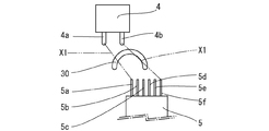
図1〜図3は本発明の一実施例を示し、同図において、1は回路基板であり、本実施例では、同一の回路構成の回路基板1を複数集合させ、その回路基板1を分割して多数個取りするため1枚の連続した大型基板1aを形成している。この回路基板1上に回路を形成した後、エッチング処理によって回路の不要部分を除去することによって回路基板1上に配線パターン2が形成される。この後、回路の必要個所にメッキ処理が行われた後、レジスト印刷により、半田付けを必要としない部分にレジストが印刷される。また、回路基板1には、電子部品としてスライドスイッチ4とフラットケーブ5が実装され、これらスライドスイッチ4とフラットケーブ5とを接続するためのランドパターン6,7が前記配線パターン2が形成される。なお、本実子例においては、ランドパターン6,7は相互に近接して段違い状に形成されているとともに、フラットケーブ5は6つの端子5a〜5fを備え、スライドスイッチ4は2つの端子4a,4bを備えている。また、スライドスイッチ4は自動半田付け機などによってランドパターン6に半田付け処理され、フラットケーブ5は後付けでランドパターン7に半田付けされる。
1 to 3 show an embodiment of the present invention. In the figure,
10は、前記ランドパターン6,7の間に形成される開口部たるスリットであり、このスリット10は、図3(b)に示すように、スライドスイッチ4とフラットケーブ5のそれぞれ両端に位置する端子4a,5a及び端子4b,5fを結んだ仮想線X1(図3(b)中、一点鎖線で示す)に掛かるように形成することが望ましいが、少なくとも、スライドスイッチ4とフラットケーブ5の最も近接する端子4b,5a同士を結んだ仮想線X2(図3(C)中、三点鎖線で示す)に掛かるように形成すればよい。なお、本実施例においては、予めランドパターン6に接続されたスライドスイッチ4の端子4bに対して最も遠い端子5fを除く5本の端子5a〜5eと2本の端子4a,4bとを結んだ仮想線X(図3(a)中、二点鎖線で示す)に掛かるようにスリット10が形成されている。
以上のように構成される本実施例においては、予めスライドスイッチ4がランドパターン6に半田付け処理され、フラットケーブ5の端子5a〜5fを後付けしてランドパターン7に半田付けする。この時、フラットケーブ5を半田付けすることによって、フラックスが発生するが、ランドパターン6,7の間には、最も遠い端子5fを除いた4本の端子5a〜5eと2本の端子4a,4bとを結んだ仮想線Xに掛かるようにスリット10が形成されているため、そのスリット10からフラックスが逃げてスライドスイッチ4内部にフラックスが侵入しにくくなる。すなわち、フラットケーブ5の端子5fとスライドスイッチ4の端子4bとは比較的離れた位置には配置されているから、端子4fの半田付け時に発生するフラックスはスライドスイッチ4に到達されにくく、スライドスイッチ4に対する影響は少ない。このように、最低限、スライドスイッチ4にフラックスが侵入しやすい部分の端子5a〜5eと端子4a,4bとの間にスリット10を形成すれば、後付けのフラットケーブル5を半田付けする際に発生するフラックスのスライドスイッチ4への侵入を効果的に防止することができ、これにより、フラックスによる電解腐食や絶縁劣化などのスライドスイッチ4の不良を防止することができるとともに、スリット10を必要最低限の長さとすることにより、回路基板1に高密度に電子部品を実装することができ、回路基板1を小型化できるばかりでなく、パターン設計の自由度も高まる。また、フラットケーブ5の半田付時に発生する熱や異物もスリット10による形成される空間部によってスライドスイッチ4に伝わりにくくなるため、熱や異物などによるスライドスイッチ4の悪影響も防止することができる。
In the present embodiment configured as described above, the
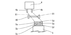
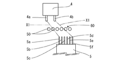
以上、本実施例の一実施例について詳述したが、本発明は、前記実施例に限定されるものではなく、本発明の要旨の範囲内で種々の変形実施が可能である。例えば、スリット10の形状は直線的な形状に限らず、例えば、図4〜図6で示すようにV字状のスリット20や半円状のスリット30あるいはH字状のスリット40を形成してもよく、スリットの形状は適宜選定すればよい。さらに、連続的なスリットに限らず例えば図7に示すように、円状の開口孔50を相互に近接させて断続的なスリット60としてもよい。また、回路基板1に実装する電子部品は、フラットケーブル5、スライドスイッチ4に限らず各種の電子部品に適用可能であるとともに、端子の個数も適宜選定すればよい。
As mentioned above, although one Example of the present Example was explained in full detail, this invention is not limited to the said Example, A various deformation | transformation implementation is possible within the range of the summary of this invention. For example, the shape of the
1 回路基板
4 スライドスイッチ(電子部品)
5 フラットケーブ(電子部品)
6,7 ランドパターン
5a〜5f フラットケーブの端子
4a,4b スライドスイッチの端子
10,20,30,40,60 スリット(開口部)
X,X1,X2 仮想線
1
5 Flat cave (electronic parts)
6,7
X, X1, X2 virtual lines
Claims (3)
Priority Applications (2)
| Application Number | Priority Date | Filing Date | Title |
|---|---|---|---|
| JP2004065100A JP2005259739A (en) | 2004-03-09 | 2004-03-09 | Substrate |
| US11/073,846 US7291912B2 (en) | 2004-03-09 | 2005-03-08 | Circuit board |
Applications Claiming Priority (1)
| Application Number | Priority Date | Filing Date | Title |
|---|---|---|---|
| JP2004065100A JP2005259739A (en) | 2004-03-09 | 2004-03-09 | Substrate |
Publications (2)
| Publication Number | Publication Date |
|---|---|
| JP2005259739A true JP2005259739A (en) | 2005-09-22 |
| JP2005259739A5 JP2005259739A5 (en) | 2006-08-10 |
Family
ID=34918217
Family Applications (1)
| Application Number | Title | Priority Date | Filing Date |
|---|---|---|---|
| JP2004065100A Withdrawn JP2005259739A (en) | 2004-03-09 | 2004-03-09 | Substrate |
Country Status (2)
| Country | Link |
|---|---|
| US (1) | US7291912B2 (en) |
| JP (1) | JP2005259739A (en) |
Cited By (1)
| Publication number | Priority date | Publication date | Assignee | Title |
|---|---|---|---|---|
| JP2016225490A (en) * | 2015-06-01 | 2016-12-28 | シャープ株式会社 | Print-circuit board and refrigerator including the same |
Family Cites Families (7)
| Publication number | Priority date | Publication date | Assignee | Title |
|---|---|---|---|---|
| JPS5571558U (en) * | 1978-11-08 | 1980-05-16 | ||
| JPH0536871U (en) | 1990-12-27 | 1993-05-18 | オリンパス光学工業株式会社 | Flexible board for circuit connection |
| JPH05110242A (en) | 1991-10-17 | 1993-04-30 | Matsushita Electric Ind Co Ltd | Board |
| JPH07114315B2 (en) | 1992-05-22 | 1995-12-06 | 富士機工電子株式会社 | Printed circuit board for mounting electronic components with narrow pitch electrodes |
| TW269705B (en) | 1992-06-15 | 1996-02-01 | Hoechst Celanese Corp | |
| US6803514B2 (en) * | 2001-03-23 | 2004-10-12 | Canon Kabushiki Kaisha | Mounting structure and mounting method of a photovoltaic element, mounting substrate for mounting a semiconductor element thereon and method for mounting a semiconductor element on said mounting substrate |
| JP2003338682A (en) * | 2002-01-11 | 2003-11-28 | Nec Infrontia Corp | Soldering method and soldered body |
-
2004
- 2004-03-09 JP JP2004065100A patent/JP2005259739A/en not_active Withdrawn
-
2005
- 2005-03-08 US US11/073,846 patent/US7291912B2/en not_active Expired - Fee Related
Cited By (1)
| Publication number | Priority date | Publication date | Assignee | Title |
|---|---|---|---|---|
| JP2016225490A (en) * | 2015-06-01 | 2016-12-28 | シャープ株式会社 | Print-circuit board and refrigerator including the same |
Also Published As
| Publication number | Publication date |
|---|---|
| US20050200010A1 (en) | 2005-09-15 |
| US7291912B2 (en) | 2007-11-06 |
Similar Documents
| Publication | Publication Date | Title |
|---|---|---|
| JP4650948B2 (en) | Through-hole soldering structure | |
| JP2009182141A (en) | Electronic apparatus and method of manufacturing the same | |
| JP2007027538A (en) | Circuit board | |
| JP2006012997A (en) | Printed board manufacturing method and printed board provided with vent hole | |
| JP2005259739A (en) | Substrate | |
| JP2006253217A (en) | Connection structure of flexible board, pickup, electronic apparatus and method of connecting flexible board | |
| JP2007207826A (en) | Printed circuit board | |
| JP2006006079A (en) | Electrical junction box | |
| JPH1197816A (en) | Printed wiring board | |
| JP2009060006A (en) | Soldering pallet | |
| JP2002009449A (en) | Printed-wiring board device | |
| JP2007123165A (en) | Circuit board with connector | |
| JP2008103393A (en) | Led lamp device | |
| JP2017175064A (en) | Electronic device and its manufacturing method | |
| JP2008112915A (en) | Circuit board connection structure | |
| JP2007242906A (en) | Printed wiring board | |
| JP2003115648A (en) | Printed circuit board and method for forming test land of printed circuit board | |
| JP2005251857A (en) | Printed circuit board and method of manufacturing the same | |
| JPH11204954A (en) | Electronic apparatus | |
| JPH08321669A (en) | Mounting structure of electronic part | |
| JP2007059569A (en) | Electronic controller | |
| JP2008227179A (en) | Printed-circuit board | |
| JP2004023082A (en) | Printed circuit board | |
| JP2009200234A (en) | Metal base substrate and method for manufacturing the same | |
| JP2006005279A (en) | Circuit board |
Legal Events
| Date | Code | Title | Description |
|---|---|---|---|
| A521 | Request for written amendment filed |
Free format text: JAPANESE INTERMEDIATE CODE: A523 Effective date: 20060623 |
|
| A621 | Written request for application examination |
Free format text: JAPANESE INTERMEDIATE CODE: A621 Effective date: 20060623 |
|
| A131 | Notification of reasons for refusal |
Free format text: JAPANESE INTERMEDIATE CODE: A131 Effective date: 20070227 |
|
| A521 | Request for written amendment filed |
Free format text: JAPANESE INTERMEDIATE CODE: A523 Effective date: 20070427 |
|
| A02 | Decision of refusal |
Free format text: JAPANESE INTERMEDIATE CODE: A02 Effective date: 20070529 |
|
| A521 | Request for written amendment filed |
Free format text: JAPANESE INTERMEDIATE CODE: A523 Effective date: 20070726 |
|
| A911 | Transfer to examiner for re-examination before appeal (zenchi) |
Free format text: JAPANESE INTERMEDIATE CODE: A911 Effective date: 20070817 |
|
| A912 | Re-examination (zenchi) completed and case transferred to appeal board |
Free format text: JAPANESE INTERMEDIATE CODE: A912 Effective date: 20070907 |
|
| A761 | Written withdrawal of application |
Free format text: JAPANESE INTERMEDIATE CODE: A761 Effective date: 20090309 |