JP2005244227A - ウエハの二次元スキャン機構 - Google Patents
ウエハの二次元スキャン機構 Download PDFInfo
- Publication number
- JP2005244227A JP2005244227A JP2005045898A JP2005045898A JP2005244227A JP 2005244227 A JP2005244227 A JP 2005244227A JP 2005045898 A JP2005045898 A JP 2005045898A JP 2005045898 A JP2005045898 A JP 2005045898A JP 2005244227 A JP2005244227 A JP 2005244227A
- Authority
- JP
- Japan
- Prior art keywords
- link
- end effector
- scanning device
- joint
- operable
- Prior art date
- Legal status (The legal status is an assumption and is not a legal conclusion. Google has not performed a legal analysis and makes no representation as to the accuracy of the status listed.)
- Withdrawn
Links
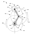
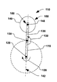
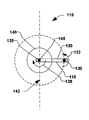
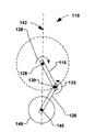
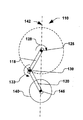
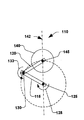
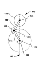
- 230000007246 mechanism Effects 0.000 title claims abstract description 38
- 239000012636 effector Substances 0.000 claims abstract description 80
- 239000000758 substrate Substances 0.000 claims abstract description 77
- 238000000034 method Methods 0.000 claims abstract description 28
- 238000012545 processing Methods 0.000 claims description 7
- 238000010884 ion-beam technique Methods 0.000 abstract description 23
- 238000002347 injection Methods 0.000 abstract 1
- 239000007924 injection Substances 0.000 abstract 1
- 239000000243 solution Substances 0.000 abstract 1
- 230000001133 acceleration Effects 0.000 description 15
- 235000012431 wafers Nutrition 0.000 description 10
- 238000005468 ion implantation Methods 0.000 description 8
- 230000008569 process Effects 0.000 description 8
- 230000008901 benefit Effects 0.000 description 4
- 238000010586 diagram Methods 0.000 description 4
- 150000002500 ions Chemical class 0.000 description 4
- 239000004065 semiconductor Substances 0.000 description 4
- 238000006243 chemical reaction Methods 0.000 description 2
- 238000010924 continuous production Methods 0.000 description 2
- 238000013461 design Methods 0.000 description 2
- 239000000463 material Substances 0.000 description 2
- 238000012546 transfer Methods 0.000 description 2
- 238000013459 approach Methods 0.000 description 1
- 230000000712 assembly Effects 0.000 description 1
- 238000000429 assembly Methods 0.000 description 1
- 238000010923 batch production Methods 0.000 description 1
- 230000003749 cleanliness Effects 0.000 description 1
- 230000000295 complement effect Effects 0.000 description 1
- 230000000694 effects Effects 0.000 description 1
- 230000010354 integration Effects 0.000 description 1
- 238000004519 manufacturing process Methods 0.000 description 1
- 238000012986 modification Methods 0.000 description 1
- 230000004048 modification Effects 0.000 description 1
- 239000003973 paint Substances 0.000 description 1
- 239000002245 particle Substances 0.000 description 1
- 230000001360 synchronised effect Effects 0.000 description 1
Images


Classifications
-
- H—ELECTRICITY
- H01—ELECTRIC ELEMENTS
- H01J—ELECTRIC DISCHARGE TUBES OR DISCHARGE LAMPS
- H01J37/00—Discharge tubes with provision for introducing objects or material to be exposed to the discharge, e.g. for the purpose of examination or processing thereof
- H01J37/30—Electron-beam or ion-beam tubes for localised treatment of objects
- H01J37/317—Electron-beam or ion-beam tubes for localised treatment of objects for changing properties of the objects or for applying thin layers thereon, e.g. for ion implantation
- H01J37/3171—Electron-beam or ion-beam tubes for localised treatment of objects for changing properties of the objects or for applying thin layers thereon, e.g. for ion implantation for ion implantation
-
- H—ELECTRICITY
- H01—ELECTRIC ELEMENTS
- H01J—ELECTRIC DISCHARGE TUBES OR DISCHARGE LAMPS
- H01J2237/00—Discharge tubes exposing object to beam, e.g. for analysis treatment, etching, imaging
- H01J2237/20—Positioning, supporting, modifying or maintaining the physical state of objects being observed or treated
- H01J2237/202—Movement
- H01J2237/20221—Translation
- H01J2237/20228—Mechanical X-Y scanning
Landscapes
- Chemical & Material Sciences (AREA)
- Analytical Chemistry (AREA)
- Container, Conveyance, Adherence, Positioning, Of Wafer (AREA)
Applications Claiming Priority (1)
| Application Number | Priority Date | Filing Date | Title |
|---|---|---|---|
| US10/786,660 US7112808B2 (en) | 2004-02-25 | 2004-02-25 | Wafer 2D scan mechanism |
Publications (2)
| Publication Number | Publication Date |
|---|---|
| JP2005244227A true JP2005244227A (ja) | 2005-09-08 |
| JP2005244227A5 JP2005244227A5 (enExample) | 2008-03-13 |
Family
ID=34861806
Family Applications (1)
| Application Number | Title | Priority Date | Filing Date |
|---|---|---|---|
| JP2005045898A Withdrawn JP2005244227A (ja) | 2004-02-25 | 2005-02-22 | ウエハの二次元スキャン機構 |
Country Status (2)
| Country | Link |
|---|---|
| US (1) | US7112808B2 (enExample) |
| JP (1) | JP2005244227A (enExample) |
Cited By (1)
| Publication number | Priority date | Publication date | Assignee | Title |
|---|---|---|---|---|
| KR102956173B1 (ko) | 2020-04-24 | 2026-04-22 | 티이엘 매뉴팩처링 앤드 엔지니어링 오브 아메리카, 인크. | 집속 빔을 처리하기 위한 웨이퍼 스캐닝 장치 및 방법 |
Families Citing this family (12)
| Publication number | Priority date | Publication date | Assignee | Title |
|---|---|---|---|---|
| US7112808B2 (en) | 2004-02-25 | 2006-09-26 | Axcelis Technologies, Inc. | Wafer 2D scan mechanism |
| DE602005021628D1 (de) * | 2004-04-05 | 2010-07-15 | Axcelis Tech Inc | Inen ionenstrahl |
| CN1943011A (zh) * | 2004-04-09 | 2007-04-04 | 艾克塞利斯技术公司 | 利用弹簧和平衡重的具有往复旋转运动的晶片扫描系统 |
| US7119343B2 (en) * | 2004-05-06 | 2006-10-10 | Axcelis Technologies, Inc. | Mechanical oscillator for wafer scan with spot beam |
| CN1291445C (zh) * | 2004-06-18 | 2006-12-20 | 清华大学 | 离子注入机中的靶盘角度控制与扫描运动机构 |
| WO2007065134A2 (en) * | 2005-12-01 | 2007-06-07 | Epion Corporation | Method and apparatus for scanning a workpiece through an ion beam |
| US20080023654A1 (en) * | 2006-07-28 | 2008-01-31 | Michael Graf | Method of reducing transient wafer temperature during implantation |
| US7582883B2 (en) * | 2007-01-12 | 2009-09-01 | Applied Materials, Inc. | Method of scanning a substrate in an ion implanter |
| US8791430B2 (en) | 2011-03-04 | 2014-07-29 | Tel Epion Inc. | Scanner for GCIB system |
| US9029808B2 (en) | 2011-03-04 | 2015-05-12 | Tel Epion Inc. | Low contamination scanner for GCIB system |
| DE112014003220B4 (de) * | 2013-07-11 | 2025-08-28 | Kla-Tencor Corporation | Konfigurationen für einen Metrologietisch und Verfahren zum Betreiben des Metrologietisches |
| TWI866681B (zh) * | 2023-12-08 | 2024-12-11 | 均華精密工業股份有限公司 | 同向式多軸作業設備 |
Family Cites Families (24)
| Publication number | Priority date | Publication date | Assignee | Title |
|---|---|---|---|---|
| US4736107A (en) | 1986-09-24 | 1988-04-05 | Eaton Corporation | Ion beam implanter scan control system |
| US5737500A (en) * | 1992-03-11 | 1998-04-07 | California Institute Of Technology | Mobile dexterous siren degree of freedom robot arm with real-time control system |
| US5486080A (en) | 1994-06-30 | 1996-01-23 | Diamond Semiconductor Group, Inc. | High speed movement of workpieces in vacuum processing |
| US5741113A (en) * | 1995-07-10 | 1998-04-21 | Kensington Laboratories, Inc. | Continuously rotatable multiple link robot arm mechanism |
| US6428266B1 (en) * | 1995-07-10 | 2002-08-06 | Brooks Automation, Inc. | Direct driven robot |
| US5746565A (en) | 1996-01-22 | 1998-05-05 | Integrated Solutions, Inc. | Robotic wafer handler |
| JP3729604B2 (ja) | 1997-06-16 | 2005-12-21 | 住友イートンノバ株式会社 | イオン注入装置 |
| US6384418B1 (en) | 1998-05-18 | 2002-05-07 | Seiko Instruments Inc. | Sample transfer apparatus and sample stage |
| GB2339959B (en) | 1998-07-21 | 2003-06-18 | Applied Materials Inc | Ion implantation beam monitor |
| US6207959B1 (en) | 1999-04-19 | 2001-03-27 | Applied Materials, Inc. | Ion implanter |
| EP1056114A3 (en) | 1999-05-24 | 2007-05-09 | Applied Materials, Inc. | Ion implantation apparatus |
| JP3976455B2 (ja) | 1999-09-17 | 2007-09-19 | 株式会社日立製作所 | イオン注入装置 |
| US6515288B1 (en) | 2000-03-16 | 2003-02-04 | Applied Materials, Inc. | Vacuum bearing structure and a method of supporting a movable member |
| US6677599B2 (en) | 2000-03-27 | 2004-01-13 | Applied Materials, Inc. | System and method for uniformly implanting a wafer with an ion beam |
| JP5072163B2 (ja) | 2000-05-15 | 2012-11-14 | バリアン・セミコンダクター・エクイップメント・アソシエイツ・インコーポレイテッド | 高能率走査イオン注入器 |
| US20020125446A1 (en) | 2001-02-20 | 2002-09-12 | Vanderpot John W. | Substrate positioning system |
| JP4061044B2 (ja) | 2001-10-05 | 2008-03-12 | 住友重機械工業株式会社 | 基板移動装置 |
| US7059817B2 (en) * | 2001-11-29 | 2006-06-13 | Axcelis Technologies, Inc. | Wafer handling apparatus and method |
| US6956223B2 (en) | 2002-04-10 | 2005-10-18 | Applied Materials, Inc. | Multi-directional scanning of movable member and ion beam monitoring arrangement therefor |
| US6908836B2 (en) | 2002-09-23 | 2005-06-21 | Applied Materials, Inc. | Method of implanting a substrate and an ion implanter for performing the method |
| GB2389958B (en) | 2002-06-21 | 2005-09-07 | Applied Materials Inc | Multi directional mechanical scanning in an ion implanter |
| US7049210B2 (en) | 2002-09-23 | 2006-05-23 | Applied Materials, Inc. | Method of implanting a substrate and an ion implanter for performing the method |
| US7112808B2 (en) | 2004-02-25 | 2006-09-26 | Axcelis Technologies, Inc. | Wafer 2D scan mechanism |
| US6953942B1 (en) | 2004-09-20 | 2005-10-11 | Axcelis Technologies, Inc. | Ion beam utilization during scanned ion implantation |
-
2004
- 2004-02-25 US US10/786,660 patent/US7112808B2/en not_active Expired - Fee Related
-
2005
- 2005-02-22 JP JP2005045898A patent/JP2005244227A/ja not_active Withdrawn
Cited By (1)
| Publication number | Priority date | Publication date | Assignee | Title |
|---|---|---|---|---|
| KR102956173B1 (ko) | 2020-04-24 | 2026-04-22 | 티이엘 매뉴팩처링 앤드 엔지니어링 오브 아메리카, 인크. | 집속 빔을 처리하기 위한 웨이퍼 스캐닝 장치 및 방법 |
Also Published As
| Publication number | Publication date |
|---|---|
| US20050184253A1 (en) | 2005-08-25 |
| US7112808B2 (en) | 2006-09-26 |
Similar Documents
| Publication | Publication Date | Title |
|---|---|---|
| US8078304B2 (en) | Dual-mode robot systems and methods for electronic device manufacturing | |
| JP5004052B2 (ja) | イオンビームの中を通過してワークピースを往復移動させるための方法 | |
| JP2005244227A (ja) | ウエハの二次元スキャン機構 | |
| JP5304979B2 (ja) | イオン注入のスキャン中に使用される改良されたイオンビーム | |
| CN101006545B (zh) | 用于使工件往复经过离子束的方法 | |
| US7119343B2 (en) | Mechanical oscillator for wafer scan with spot beam | |
| JP2008519417A (ja) | スキャンされるイオン注入中での線量を一様にする改善 | |
| JP4840607B2 (ja) | ばねと釣合重りを用いて往復回転運動を行うウエハ走査システム | |
| TWI610348B (zh) | 電極調整組件與調整電極的方法 | |
| JP2024519460A (ja) | ウエハセンタリング機能を備えた回転インデクサ | |
| KR102717630B1 (ko) | 얼라인먼트 스테이지, 이를 이용한 이송시스템 및 얼라인 방법 | |
| WO2006121431A1 (en) | Mechanical oscillator for wafer scan with spot beam | |
| JP7315905B2 (ja) | 基板移送装置 | |
| JP2008047525A (ja) | イオン注入中にウエハ温度を一時的に低下させる方法 |
Legal Events
| Date | Code | Title | Description |
|---|---|---|---|
| A521 | Request for written amendment filed |
Free format text: JAPANESE INTERMEDIATE CODE: A523 Effective date: 20080125 |
|
| A621 | Written request for application examination |
Free format text: JAPANESE INTERMEDIATE CODE: A621 Effective date: 20080125 |
|
| A761 | Written withdrawal of application |
Free format text: JAPANESE INTERMEDIATE CODE: A761 Effective date: 20091105 |