JP2005150283A - Bga package - Google Patents
Bga package Download PDFInfo
- Publication number
- JP2005150283A JP2005150283A JP2003383617A JP2003383617A JP2005150283A JP 2005150283 A JP2005150283 A JP 2005150283A JP 2003383617 A JP2003383617 A JP 2003383617A JP 2003383617 A JP2003383617 A JP 2003383617A JP 2005150283 A JP2005150283 A JP 2005150283A
- Authority
- JP
- Japan
- Prior art keywords
- bga package
- pads
- pad
- bypass capacitor
- printed wiring
- Prior art date
- Legal status (The legal status is an assumption and is not a legal conclusion. Google has not performed a legal analysis and makes no representation as to the accuracy of the status listed.)
- Pending
Links
Images


Classifications
-
- H—ELECTRICITY
- H01—ELECTRIC ELEMENTS
- H01L—SEMICONDUCTOR DEVICES NOT COVERED BY CLASS H10
- H01L2224/00—Indexing scheme for arrangements for connecting or disconnecting semiconductor or solid-state bodies and methods related thereto as covered by H01L24/00
- H01L2224/01—Means for bonding being attached to, or being formed on, the surface to be connected, e.g. chip-to-package, die-attach, "first-level" interconnects; Manufacturing methods related thereto
- H01L2224/10—Bump connectors; Manufacturing methods related thereto
- H01L2224/15—Structure, shape, material or disposition of the bump connectors after the connecting process
- H01L2224/16—Structure, shape, material or disposition of the bump connectors after the connecting process of an individual bump connector
- H01L2224/161—Disposition
- H01L2224/16151—Disposition the bump connector connecting between a semiconductor or solid-state body and an item not being a semiconductor or solid-state body, e.g. chip-to-substrate, chip-to-passive
- H01L2224/16221—Disposition the bump connector connecting between a semiconductor or solid-state body and an item not being a semiconductor or solid-state body, e.g. chip-to-substrate, chip-to-passive the body and the item being stacked
- H01L2224/16225—Disposition the bump connector connecting between a semiconductor or solid-state body and an item not being a semiconductor or solid-state body, e.g. chip-to-substrate, chip-to-passive the body and the item being stacked the item being non-metallic, e.g. insulating substrate with or without metallisation
-
- H—ELECTRICITY
- H01—ELECTRIC ELEMENTS
- H01L—SEMICONDUCTOR DEVICES NOT COVERED BY CLASS H10
- H01L2224/00—Indexing scheme for arrangements for connecting or disconnecting semiconductor or solid-state bodies and methods related thereto as covered by H01L24/00
- H01L2224/01—Means for bonding being attached to, or being formed on, the surface to be connected, e.g. chip-to-package, die-attach, "first-level" interconnects; Manufacturing methods related thereto
- H01L2224/10—Bump connectors; Manufacturing methods related thereto
- H01L2224/15—Structure, shape, material or disposition of the bump connectors after the connecting process
- H01L2224/16—Structure, shape, material or disposition of the bump connectors after the connecting process of an individual bump connector
- H01L2224/161—Disposition
- H01L2224/16151—Disposition the bump connector connecting between a semiconductor or solid-state body and an item not being a semiconductor or solid-state body, e.g. chip-to-substrate, chip-to-passive
- H01L2224/16221—Disposition the bump connector connecting between a semiconductor or solid-state body and an item not being a semiconductor or solid-state body, e.g. chip-to-substrate, chip-to-passive the body and the item being stacked
- H01L2224/16265—Disposition the bump connector connecting between a semiconductor or solid-state body and an item not being a semiconductor or solid-state body, e.g. chip-to-substrate, chip-to-passive the body and the item being stacked the item being a discrete passive component
-
- H—ELECTRICITY
- H01—ELECTRIC ELEMENTS
- H01L—SEMICONDUCTOR DEVICES NOT COVERED BY CLASS H10
- H01L2924/00—Indexing scheme for arrangements or methods for connecting or disconnecting semiconductor or solid-state bodies as covered by H01L24/00
- H01L2924/15—Details of package parts other than the semiconductor or other solid state devices to be connected
- H01L2924/151—Die mounting substrate
- H01L2924/153—Connection portion
- H01L2924/1531—Connection portion the connection portion being formed only on the surface of the substrate opposite to the die mounting surface
- H01L2924/15311—Connection portion the connection portion being formed only on the surface of the substrate opposite to the die mounting surface being a ball array, e.g. BGA
-
- H—ELECTRICITY
- H01—ELECTRIC ELEMENTS
- H01L—SEMICONDUCTOR DEVICES NOT COVERED BY CLASS H10
- H01L2924/00—Indexing scheme for arrangements or methods for connecting or disconnecting semiconductor or solid-state bodies as covered by H01L24/00
- H01L2924/19—Details of hybrid assemblies other than the semiconductor or other solid state devices to be connected
- H01L2924/191—Disposition
- H01L2924/19101—Disposition of discrete passive components
- H01L2924/19102—Disposition of discrete passive components in a stacked assembly with the semiconductor or solid state device
- H01L2924/19103—Disposition of discrete passive components in a stacked assembly with the semiconductor or solid state device interposed between the semiconductor or solid-state device and the die mounting substrate, i.e. chip-on-passive
-
- H—ELECTRICITY
- H01—ELECTRIC ELEMENTS
- H01L—SEMICONDUCTOR DEVICES NOT COVERED BY CLASS H10
- H01L2924/00—Indexing scheme for arrangements or methods for connecting or disconnecting semiconductor or solid-state bodies as covered by H01L24/00
- H01L2924/19—Details of hybrid assemblies other than the semiconductor or other solid state devices to be connected
- H01L2924/191—Disposition
- H01L2924/19101—Disposition of discrete passive components
- H01L2924/19102—Disposition of discrete passive components in a stacked assembly with the semiconductor or solid state device
- H01L2924/19104—Disposition of discrete passive components in a stacked assembly with the semiconductor or solid state device on the semiconductor or solid-state device, i.e. passive-on-chip
-
- H—ELECTRICITY
- H01—ELECTRIC ELEMENTS
- H01L—SEMICONDUCTOR DEVICES NOT COVERED BY CLASS H10
- H01L2924/00—Indexing scheme for arrangements or methods for connecting or disconnecting semiconductor or solid-state bodies as covered by H01L24/00
- H01L2924/19—Details of hybrid assemblies other than the semiconductor or other solid state devices to be connected
- H01L2924/191—Disposition
- H01L2924/19101—Disposition of discrete passive components
- H01L2924/19105—Disposition of discrete passive components in a side-by-side arrangement on a common die mounting substrate
Landscapes
- Structures For Mounting Electric Components On Printed Circuit Boards (AREA)
Abstract
Description
本発明は、内部に半導体ICを収容し、底面に他の装置との接続のための複数のパッドが設けられたBGAパッケージに関する。 The present invention relates to a BGA package in which a semiconductor IC is accommodated and a plurality of pads are provided on the bottom surface for connection to other devices.
プリント配線基板にデバイスを実装するために、表面実装デバイスが用いられる。表面実装デバイスとして、図6に示すようなBGA(Ball Grid Array)パッケージの半導体デバイスがある。図において、BGAパッケージ1の下面には、パッド3が格子状に設けられ、更に、端子3には、はんだボール5が付着されている。 A surface mount device is used to mount the device on a printed wiring board. As a surface mount device, there is a BGA (Ball Grid Array) package semiconductor device as shown in FIG. In the figure, pads 3 are provided in a lattice pattern on the lower surface of the BGA package 1, and solder balls 5 are attached to the terminals 3.
一方、プリント配線基板(PCB)7には、BGAパッケージ1のパッド3と対応するパッド9が設けられている。そして、はんだボール5がプリント配線基板7のパッド9に接するようにBGAパッケージ1を配置し、外部から熱を加えてはんだボール5を融解し、BGAパッケージ1をプリント配線基板7に実装する。装置全体が小型化しつつある現状においては、BGAパッケージが広く使用されつつある。 On the other hand, the printed wiring board (PCB) 7 is provided with pads 9 corresponding to the pads 3 of the BGA package 1. Then, the BGA package 1 is arranged so that the solder balls 5 are in contact with the pads 9 of the printed wiring board 7, heat is applied from the outside to melt the solder balls 5, and the BGA package 1 is mounted on the printed wiring board 7. In the present situation where the entire apparatus is becoming smaller, BGA packages are being widely used.
一方、デジタル回路や高周波回路等のような高速な動作クロックを用いて作動する半導体デバイスがプリント配線基板に実装された場合には、電源ラインに電流変動ノイズが発生し、半導体デバイスに悪影響が及ぶことがある。そのため、ノイズ除去のために、半導体デバイスの電力供給端子の近傍にバイパスコンデンサ(パスコン)を設けることがある。 On the other hand, when a semiconductor device that operates using a high-speed operation clock such as a digital circuit or a high-frequency circuit is mounted on a printed wiring board, current fluctuation noise occurs in the power supply line, which adversely affects the semiconductor device. Sometimes. Therefore, a bypass capacitor (pass capacitor) may be provided in the vicinity of the power supply terminal of the semiconductor device in order to eliminate noise.
図7にその一例を示す。図はBGAパッケージ11が実装されたプリント配線基板13の裏面を示している。破線で示す15はBGAパッケージ11のパッドである。又、実線で示す17は、プリント配線基板13の表面と裏面とを配線するビアホール(Via Hole)である。このビアホール17を用いてプリント配線基板13の裏面に、バイパスコンデンサ19が接続されている。 An example is shown in FIG. The figure shows the back surface of the printed wiring board 13 on which the BGA package 11 is mounted. Reference numeral 15 indicated by a broken line denotes a pad of the BGA package 11. Reference numeral 17 shown by a solid line is a via hole for wiring the front surface and the back surface of the printed wiring board 13. A bypass capacitor 19 is connected to the back surface of the printed wiring board 13 using the via hole 17.
しかし、信号ラインとの関係でビアホール17によりプリント配線基板の裏面まで配線できる電源ラインには制限があり、BGAパッケージ11の周縁にもバイパスコンデンサ19′を設けている。 However, there is a limit to the power supply line that can be wired to the back surface of the printed wiring board through the via hole 17 in relation to the signal line, and a bypass capacitor 19 ′ is also provided at the periphery of the BGA package 11.
バイパスコンデンサは、電源ラインに可能な限り近く設けることが必要で、BGAパッケージ11の周縁に設けたバイパスコンデンサ19′は、ノイズ除去効果があまり期待できない。又、プリント配線基板13も大きくなる。 The bypass capacitor must be provided as close as possible to the power supply line, and the bypass capacitor 19 ′ provided at the periphery of the BGA package 11 cannot be expected to have a noise removal effect. Moreover, the printed wiring board 13 is also enlarged.
そこで、BGAパッケージの場合、以下のような方法で、バイパスコンデンサを設けることが提案されている。
(1)BGAパッケージ内にバイパスコンデンサを設ける。
Therefore, in the case of the BGA package, it has been proposed to provide a bypass capacitor by the following method.
(1) A bypass capacitor is provided in the BGA package.
図8に示すように、半導体IC(チップ)21はサブ基板23上に設けられ、サブ基板23には、半導体IC21を覆い、半導体IC21の上面に当接する蓋状の放熱板25が設けられている。サブ基板23の下面には、他の装置との接続のための複数のパッド27が設けられ、更に、各パッド27には、はんだボール29が付着されている。そして、バイパスコンデンサ31がサブ基板23上に設けられている。
(2)BGAパッケージの上面にバイパスコンデンサを搭載する(例えば、特許文献1参照。)。
(2) A bypass capacitor is mounted on the top surface of the BGA package (see, for example, Patent Document 1).
しかし、上述した(1)(2)のような方法では、以下のような問題点がある。
(1)半導体IC1の面積が大きくなると、サブ基板23にバイパスコンデンサ31を設けるスペースがなくなる。バイパスコンデンサ31をサブ基板23にどうしても設けようとすると、BGAパッケージが大形化し、プリント配線基板も大形化する。
(2)BGAパッケージの上面に放熱フィンや放熱ファンを載せる場合は、バイパスコンデンサは搭載できない。
However, the methods (1) and (2) described above have the following problems.
(1) When the area of the semiconductor IC 1 is increased, there is no space for providing the bypass capacitor 31 on the sub-board 23. If the bypass capacitor 31 is inevitably provided on the sub-board 23, the BGA package is enlarged and the printed wiring board is also enlarged.
(2) When a heat radiating fin or a heat radiating fan is placed on the upper surface of the BGA package, a bypass capacitor cannot be mounted.
又、バイパスコンデンサの代わりに、電気的特性の向上のために抵抗やコイル等の回路部品を用いる場合であっても、上述の(1)、(2)に示す方法が可能であるが、同様な問題点が生じる。 Even when circuit components such as resistors and coils are used to improve electrical characteristics instead of bypass capacitors, the methods shown in the above (1) and (2) are possible. Problems arise.
本発明は、上記問題点に鑑みてなされたもので、その課題は、電気的特性の向上、小型化が図れるBGAパッケージを提供することにある。 The present invention has been made in view of the above problems, and an object thereof is to provide a BGA package capable of improving electrical characteristics and reducing the size.
上記課題を解決する請求項1に係る発明は、内部に半導体ICを収容し、底面に他の装置との接続のための複数のパッドが設けられたBGAパッケージにおいて、前記複数のパッドのうちの少なくとも1つに、回路部品が接続されたことを特徴とするBGAパッケージである。 The invention according to claim 1, which solves the above problem, is a BGA package in which a semiconductor IC is housed and a plurality of pads are provided on the bottom surface for connection to other devices. A BGA package is characterized in that at least one circuit component is connected.
他の装置としては、プリント配線基板等があるが限定するものではない。 Other devices include, but are not limited to, a printed wiring board.
請求項2に係る発明は、前記回路部品の一方の端子は、前記BGAパッケージのパッドに接続され、他方の端子は前記他の装置に接続されることを特徴とする請求項1記載のBGAパッケージである。 The invention according to claim 2 is the BGA package according to claim 1, wherein one terminal of the circuit component is connected to a pad of the BGA package, and the other terminal is connected to the other device. It is.
請求項3に係る発明は、前記回路部品は、前記BGAパッケージの複数のパッドのうちの隣接するパッド間に接続されることを特徴とする請求項1記載のBGAパッケージである。 The invention according to claim 3 is the BGA package according to claim 1, wherein the circuit component is connected between adjacent pads of the plurality of pads of the BGA package.
請求項4に係る発明は、前記回路部品は複数あることを特徴とする請求項1乃至3のいずれかに記載のBGAパッケージである。 The invention according to claim 4 is the BGA package according to any one of claims 1 to 3, wherein there are a plurality of the circuit components.
請求項5に係る発明は、前記回路部品は、前記回路部品は、バイパスコンデンサ、抵抗、コイルのうちの少なくとも1つであることを特徴とする請求項1乃至4のいずれかに記載のBGAパッケージである。 The invention according to claim 5 is the BGA package according to any one of claims 1 to 4, wherein the circuit component is at least one of a bypass capacitor, a resistor, and a coil. It is.
請求項1に係る発明によれば、前記複数のパッドのうちの少なくとも1つに、回路部品が接続されることにより、BGAパッケージの電気的特性の向上を図れ、BGAパッケージ、及びBGAパッケージが実装される装置の小型化が図れる。 According to the first aspect of the present invention, a circuit component is connected to at least one of the plurality of pads to improve the electrical characteristics of the BGA package, and the BGA package and the BGA package are mounted. Downsizing of the device can be achieved.
請求項2に係る発明によれば、前記回路部品の一方の端子は、前記BGAパッケージのパッドに接続され、他方の端子は前記他の装置に接続されることにより、BGAパッケージの電気的特性の向上を図れ、BGAパッケージ、及びBGAパッケージが実装される装置の小型化が図れる。 According to the invention of claim 2, one terminal of the circuit component is connected to the pad of the BGA package, and the other terminal is connected to the other device. Improvement can be achieved, and the BGA package and the device on which the BGA package is mounted can be reduced in size.
請求項3に係る発明によれば、前記回路部品は、前記BGAパッケージの複数のパッドのうちの隣接するパッド間に接続されることにより、BGAパッケージの電気的特性の向上を図れ、BGAパッケージ、及びBGAパッケージが実装される装置の小型化が図れる。 According to the invention of claim 3, the circuit component is connected between adjacent pads of the plurality of pads of the BGA package, so that the electrical characteristics of the BGA package can be improved. In addition, the apparatus on which the BGA package is mounted can be reduced in size.
請求項4に係る発明によれば、前記回路部品は複数あることにより、BGAパッケージの実装時に、はんだボールのつぶれによる実装不良を防止することができる。 According to the fourth aspect of the present invention, since there are a plurality of the circuit components, it is possible to prevent mounting failure due to collapse of the solder balls when mounting the BGA package.
請求項5に係る発明によれば、前記回路部品は、前記回路部品は、バイパスコンデンサ、抵抗、コイルのうちの少なくとも1つであることにより、BGAパッケージの電気的特性の向上を図れ、BGAパッケージ、及びBGAパッケージが実装される装置の小型化が図れる。 According to the invention of claim 5, the circuit component is at least one of a bypass capacitor, a resistor, and a coil, so that the electrical characteristics of the BGA package can be improved. And a device on which the BGA package is mounted can be reduced in size.
以下、図面を用いて本発明を実施するための最良の形態を説明する。
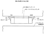
(第1の形態例請求項1,2,4,5に対応)
第1の形態例の構成図である図1、図1のA部分の拡大図である図2を用いて説明する。図において、BGAパッケージ51の下面には、複数のパッド53が格子状に設けられている。複数のパッド53のうちの少なくとも1つ、本形態例では、両サイドのパッド53′以外のパッド53には、はんだボール55が付着されている。両サイドのパッド53′(本実形態例では、電源ライン(Vcc)である)には、回路部品、本形態例では、バイパスコンデンサ57がはんだ59を用いて実装されている。
Hereinafter, the best mode for carrying out the present invention will be described with reference to the drawings.
(Corresponding to the first embodiment claim 1, 2, 4, 5)
Description will be made with reference to FIG. 1 which is a configuration diagram of the first embodiment and FIG. 2 which is an enlarged view of a portion A in FIG. In the figure, a plurality of
一方、プリント配線基板(PCB)61には、BGAパッケージ51のパッド53、パッド53′と対応するパッド63、パッド63′が設けられている。本実形態例では、パッド63′は接地ライン(GND)である。又、バイパスコンデンサ57のパッド63′と対向する部分には、はんだ65が付着している。
On the other hand, a printed wiring board (PCB) 61 is provided with a
そして、はんだボール55がプリント配線基板61のパッド63に接するように、又、バイパスコンデンサ57のはんだ65がプリント配線基板61のパッド63′に接するようにBGAパッケージ51を配置し、外部から熱を加えてはんだボール55、はんだ65を融解することにより、BGAパッケージ51はプリント配線基板61に実装されている。
Then, the BGA package 51 is arranged so that the solder balls 55 are in contact with the
このような構成によれば、以下のような効果を得ることができる。
(1)BGAパッケージ51の複数のパッドのうちの電源ラインであるパッド53′に、バイパスコンデンサ(回路部品)57が接続されることにより、ノイズの効果的な低減(電気的特性の向上)及びBGAパッケージ51、プリント配線基板61の小型化が図れる。
(2)バイパスコンデンサ57を複数設けたことにより、BGAパッケージ51が熱により撓む場合、例えば、図1において、二点鎖線で示すように変形しても、はんだボール55より圧縮や引張に対して変形しにくいバイパスコンデンサ57を複数実装したことにより、はんだボール55が圧縮されてショートしたり、引っ張られて切断され、電気的導通がなくなったりすることが防止できる。
According to such a configuration, the following effects can be obtained.
(1) By connecting a bypass capacitor (circuit component) 57 to a
(2) When the BGA package 51 is bent due to heat by providing a plurality of
尚、本発明は、上記形態例に限定するものではない。上記形態例では、回路部品としてバイパスコンデンサ57を用いた例で説明を行ったが、他に抵抗やコイル等の回路部品であってもよい。又、バイパスコンデンサ57を複数設けたが、1つであってもよい。
The present invention is not limited to the above embodiment. In the above embodiment, the example in which the
(第2の形態例請求項1,3,5に対応)
第2の形態例の構成図である図3、図3のB部分の拡大図である図4を用いて説明する。図において、BGAパッケージ101の下面には、複数のパッド103が格子状に設けられている。複数のパッド103のうちの隣接するパッド103′、パッド103″以外のパッド103には、はんだボール105が付着されている。尚、本形態例では、パッド103′は電源ライン(Vcc)、パッド103″は接地ライン(GND)に接続されている。
(Corresponding to claims 1, 3, and 5 of the second embodiment)
This will be described with reference to FIG. 3 which is a configuration diagram of the second embodiment and FIG. 4 which is an enlarged view of a portion B in FIG. In the figure, a plurality of
パッド103′、パッド103″間には、回路部品、本形態例では、バイパスコンデンサ107がはんだ109、はんだ111を用いて実装されている。
Between the
一方、プリント配線基板(PCB)113には、BGAパッケージ101のパッド103と対応するパッド115が設けられている。
On the other hand, the printed wiring board (PCB) 113 is provided with pads 115 corresponding to the
そして、はんだボール105がプリント配線基板113のパッド115に接するようにBGAパッケージ101を配置し、外部から熱を加えてはんだボール105を融解することにより、BGAパッケージ101はプリント配線基板113に実装されている。
The BGA package 101 is mounted on the printed wiring board 113 by disposing the BGA package 101 so that the
このような構成によれば、以下のような効果を得ることができる。
(1)BGAパッケージ101の複数のパッドのうちの隣り合うパッド(Vcc)103′、パッド(GND)103″に、バイパスコンデンサ(回路部品)107が接続されることにより、ノイズの効果的な低減(電気的特性の向上)及びBGAパッケージ101、プリント配線基板113の小型化が図れる。
According to such a configuration, the following effects can be obtained.
(1) By connecting a bypass capacitor (circuit component) 107 to adjacent pads (Vcc) 103 ′ and pads (GND) 103 ″ of a plurality of pads of the BGA package 101, noise can be effectively reduced. (Improvement of electrical characteristics) and downsizing of the BGA package 101 and the printed wiring board 113 can be achieved.
尚、本発明は、上記形態例に限定するものではない。上記実施の形態例では、バイパスコンデンサ107はBGAパッケージ101のパッド(Vcc)103′、パッド(GND)103″に実装したが、更に、図5に示すように、プリント配線基板113に、BGAパッケージ101のパッド(Vcc)103′に対応し、プリント配線基板113の電源ラインに接続されるパッド105′と、BGAパッケージ101のパッド(GND)103″に対応し、プリント配線基板113の接地ラインに接続されるパッド105″とを設け、パッド105′とははんだ119を用いて、パッド105″とははんだ121を用いてバイパスコンデンサと接続するようにしてもよい。
The present invention is not limited to the above embodiment. In the above embodiment, the bypass capacitor 107 is mounted on the pad (Vcc) 103 ′ and the pad (GND) 103 ″ of the BGA package 101. Further, as shown in FIG. 101 corresponding to the pad (Vcc) 103 ′ of the pad 101 ′ connected to the power supply line of the printed wiring board 113 and the pad (GND) 103 ″ of the BGA package 101 corresponding to the ground line of the printed wiring board 113. A
又、上記形態例では、回路部品としてバイパスコンデンサ107を用いた例で説明を行ったが、他に抵抗やコイル等の回路部品であってもよい。又、バイパスコンデンサ107を複数設けてもよい。 In the above-described embodiment, the example in which the bypass capacitor 107 is used as the circuit component has been described. However, other circuit components such as a resistor and a coil may be used. A plurality of bypass capacitors 107 may be provided.
51 BGAパッケージ
53,53′,63,63′ パッド
55 はんだボール
57 バイパスコンデンサ
61 プリント配線基板
51
Claims (5)
前記複数のパッドのうちの少なくとも1つに、回路部品が接続されたことを特徴とするBGAパッケージ。 In a BGA package in which a semiconductor IC is accommodated inside and a plurality of pads are provided on the bottom surface for connection to other devices.
A BGA package, wherein a circuit component is connected to at least one of the plurality of pads.
Priority Applications (1)
| Application Number | Priority Date | Filing Date | Title |
|---|---|---|---|
| JP2003383617A JP2005150283A (en) | 2003-11-13 | 2003-11-13 | Bga package |
Applications Claiming Priority (1)
| Application Number | Priority Date | Filing Date | Title |
|---|---|---|---|
| JP2003383617A JP2005150283A (en) | 2003-11-13 | 2003-11-13 | Bga package |
Publications (2)
| Publication Number | Publication Date |
|---|---|
| JP2005150283A true JP2005150283A (en) | 2005-06-09 |
| JP2005150283A5 JP2005150283A5 (en) | 2006-11-24 |
Family
ID=34692286
Family Applications (1)
| Application Number | Title | Priority Date | Filing Date |
|---|---|---|---|
| JP2003383617A Pending JP2005150283A (en) | 2003-11-13 | 2003-11-13 | Bga package |
Country Status (1)
| Country | Link |
|---|---|
| JP (1) | JP2005150283A (en) |
Cited By (7)
| Publication number | Priority date | Publication date | Assignee | Title |
|---|---|---|---|---|
| JP2007173669A (en) * | 2005-12-26 | 2007-07-05 | Murata Mfg Co Ltd | Multilayered circuit board and integrated circuit package |
| JP2007250928A (en) * | 2006-03-17 | 2007-09-27 | Mitsubishi Electric Corp | Multilayer printed wiring board |
| US9847299B2 (en) | 2014-09-30 | 2017-12-19 | Murata Manufacturing Co., Ltd. | Semiconductor package and mounting structure thereof |
| JP2020520121A (en) * | 2017-05-15 | 2020-07-02 | エイブイエックス コーポレイション | Multilayer capacitor and circuit board including multilayer capacitor |
| WO2020250947A1 (en) * | 2019-06-14 | 2020-12-17 | キヤノン株式会社 | Semiconductor module manufacturing method, electronic device manufacturing method, semiconductor module, and electronic device |
| WO2023022047A1 (en) * | 2021-08-20 | 2023-02-23 | 株式会社村田製作所 | High-frequency module |
| JP7566054B2 (en) | 2020-07-01 | 2024-10-11 | インターナショナル・ビジネス・マシーンズ・コーポレーション | Solder Column Grid Array Capacitors |
-
2003
- 2003-11-13 JP JP2003383617A patent/JP2005150283A/en active Pending
Cited By (11)
| Publication number | Priority date | Publication date | Assignee | Title |
|---|---|---|---|---|
| JP2007173669A (en) * | 2005-12-26 | 2007-07-05 | Murata Mfg Co Ltd | Multilayered circuit board and integrated circuit package |
| JP2007250928A (en) * | 2006-03-17 | 2007-09-27 | Mitsubishi Electric Corp | Multilayer printed wiring board |
| US9847299B2 (en) | 2014-09-30 | 2017-12-19 | Murata Manufacturing Co., Ltd. | Semiconductor package and mounting structure thereof |
| JP2020520121A (en) * | 2017-05-15 | 2020-07-02 | エイブイエックス コーポレイション | Multilayer capacitor and circuit board including multilayer capacitor |
| JP2020520122A (en) * | 2017-05-15 | 2020-07-02 | エイブイエックス コーポレイション | Multilayer capacitor and circuit board including multilayer capacitor |
| US11636978B2 (en) | 2017-05-15 | 2023-04-25 | KYOCERA AVX Components Corporation | Multilayer capacitor and circuit board containing the same |
| US12112891B2 (en) | 2017-05-15 | 2024-10-08 | KYOCERA AVX Components Corporation | Multilayer capacitor and circuit board containing the same |
| WO2020250947A1 (en) * | 2019-06-14 | 2020-12-17 | キヤノン株式会社 | Semiconductor module manufacturing method, electronic device manufacturing method, semiconductor module, and electronic device |
| US20220102330A1 (en) * | 2019-06-14 | 2022-03-31 | Canon Kabushiki Kaisha | Semiconductor module manufacturing method, electronic equipment manufacturing method, semiconductor module, and electronic equipment |
| JP7566054B2 (en) | 2020-07-01 | 2024-10-11 | インターナショナル・ビジネス・マシーンズ・コーポレーション | Solder Column Grid Array Capacitors |
| WO2023022047A1 (en) * | 2021-08-20 | 2023-02-23 | 株式会社村田製作所 | High-frequency module |
Similar Documents
| Publication | Publication Date | Title |
|---|---|---|
| US10438873B2 (en) | Semiconductor chip package having heat dissipating structure | |
| JP2004071670A (en) | Ic package, connecting structure and electronic apparatus | |
| JP3894091B2 (en) | IC chip built-in multilayer substrate and manufacturing method thereof | |
| JP2007207802A (en) | Electronic circuit module and method of manufacturing same | |
| JP4987231B2 (en) | Thermally conductive substrate package | |
| JP2005150283A (en) | Bga package | |
| JP4919689B2 (en) | Module board | |
| JP2801810B2 (en) | Resin-sealed semiconductor device | |
| US6894385B1 (en) | Integrated circuit package having bypass capacitors coupled to bottom of package substrate and supporting surface mounting technology | |
| JP2005228811A (en) | Semiconductor device | |
| JP2005166892A (en) | Stack type small-sized memory card | |
| KR20080004734A (en) | Radiating structure in exothermic element | |
| JP2009129960A (en) | Semiconductor device and its manufacturing method | |
| JP2007221133A (en) | Integrated circuit package | |
| JP2006049720A (en) | Electronic circuit device | |
| JP2007165445A (en) | Power amplifier module | |
| JP2005277115A (en) | Chip capacitor mounting structure and printed wiring board | |
| JP3185456U (en) | Printed wiring board that suppresses component mounting failure due to excess solder | |
| JP5642559B2 (en) | Electronic component module | |
| JP2005191411A (en) | High frequency integrated circuit device | |
| JP4545537B2 (en) | Semiconductor device and semiconductor device unit | |
| JP2006261464A (en) | Mounting structure of electronic component, recording device provided with this mounting structure, electronic equipment and method of mounting electronic component | |
| JP2009212355A (en) | Printed circuit board and electronic circuit module | |
| JP2013038119A (en) | Attachment structure of module | |
| JP2003188292A (en) | Semiconductor device |
Legal Events
| Date | Code | Title | Description |
|---|---|---|---|
| A521 | Written amendment |
Free format text: JAPANESE INTERMEDIATE CODE: A523 Effective date: 20061005 |
|
| A621 | Written request for application examination |
Free format text: JAPANESE INTERMEDIATE CODE: A621 Effective date: 20061005 |
|
| A977 | Report on retrieval |
Free format text: JAPANESE INTERMEDIATE CODE: A971007 Effective date: 20080501 |
|
| A131 | Notification of reasons for refusal |
Free format text: JAPANESE INTERMEDIATE CODE: A131 Effective date: 20090714 |
|
| A02 | Decision of refusal |
Free format text: JAPANESE INTERMEDIATE CODE: A02 Effective date: 20091215 |