JP2005136386A - Silicon carbide-oxide laminate, manufacturing method therefor, and semiconductor device - Google Patents
Silicon carbide-oxide laminate, manufacturing method therefor, and semiconductor device Download PDFInfo
- Publication number
- JP2005136386A JP2005136386A JP2004271321A JP2004271321A JP2005136386A JP 2005136386 A JP2005136386 A JP 2005136386A JP 2004271321 A JP2004271321 A JP 2004271321A JP 2004271321 A JP2004271321 A JP 2004271321A JP 2005136386 A JP2005136386 A JP 2005136386A
- Authority
- JP
- Japan
- Prior art keywords
- silicon carbide
- oxide
- group
- oxide layer
- layer
- Prior art date
- Legal status (The legal status is an assumption and is not a legal conclusion. Google has not performed a legal analysis and makes no representation as to the accuracy of the status listed.)
- Withdrawn
Links
- 229910052710 silicon Inorganic materials 0.000 title claims abstract description 48
- XUIMIQQOPSSXEZ-UHFFFAOYSA-N Silicon Chemical compound [Si] XUIMIQQOPSSXEZ-UHFFFAOYSA-N 0.000 title claims abstract description 47
- 239000010703 silicon Substances 0.000 title claims abstract description 47
- 238000004519 manufacturing process Methods 0.000 title claims abstract description 37
- 239000004065 semiconductor Substances 0.000 title claims abstract description 11
- 229910010271 silicon carbide Inorganic materials 0.000 claims abstract description 81
- IJGRMHOSHXDMSA-UHFFFAOYSA-N Atomic nitrogen Chemical compound N#N IJGRMHOSHXDMSA-UHFFFAOYSA-N 0.000 claims abstract description 75
- 239000007789 gas Substances 0.000 claims abstract description 75
- HBMJWWWQQXIZIP-UHFFFAOYSA-N silicon carbide Chemical compound [Si+]#[C-] HBMJWWWQQXIZIP-UHFFFAOYSA-N 0.000 claims abstract description 72
- 229910021478 group 5 element Inorganic materials 0.000 claims abstract description 65
- 229910052757 nitrogen Inorganic materials 0.000 claims abstract description 40
- 239000012298 atmosphere Substances 0.000 claims abstract description 33
- 230000003647 oxidation Effects 0.000 claims abstract description 15
- 238000007254 oxidation reaction Methods 0.000 claims abstract description 15
- 239000011261 inert gas Substances 0.000 claims abstract description 11
- 238000000034 method Methods 0.000 claims description 28
- 238000000137 annealing Methods 0.000 claims description 20
- 239000012535 impurity Substances 0.000 claims description 17
- OAICVXFJPJFONN-UHFFFAOYSA-N Phosphorus Chemical compound [P] OAICVXFJPJFONN-UHFFFAOYSA-N 0.000 claims description 11
- 229910052698 phosphorus Inorganic materials 0.000 claims description 11
- 239000011574 phosphorus Substances 0.000 claims description 11
- 229910004298 SiO 2 Inorganic materials 0.000 claims description 7
- 238000009792 diffusion process Methods 0.000 claims description 7
- 238000009826 distribution Methods 0.000 claims description 4
- 238000005530 etching Methods 0.000 claims description 4
- 230000001590 oxidative effect Effects 0.000 claims description 4
- 239000000463 material Substances 0.000 claims description 3
- QJGQUHMNIGDVPM-UHFFFAOYSA-N nitrogen group Chemical group [N] QJGQUHMNIGDVPM-UHFFFAOYSA-N 0.000 claims description 3
- 238000000151 deposition Methods 0.000 claims 1
- 239000000758 substrate Substances 0.000 abstract description 27
- 230000007423 decrease Effects 0.000 abstract description 3
- VYPSYNLAJGMNEJ-UHFFFAOYSA-N Silicium dioxide Chemical compound O=[Si]=O VYPSYNLAJGMNEJ-UHFFFAOYSA-N 0.000 description 24
- 239000003990 capacitor Substances 0.000 description 12
- 235000012239 silicon dioxide Nutrition 0.000 description 12
- 239000000377 silicon dioxide Substances 0.000 description 12
- QVGXLLKOCUKJST-UHFFFAOYSA-N atomic oxygen Chemical compound [O] QVGXLLKOCUKJST-UHFFFAOYSA-N 0.000 description 8
- 230000000694 effects Effects 0.000 description 8
- 239000001301 oxygen Substances 0.000 description 8
- 229910052760 oxygen Inorganic materials 0.000 description 8
- 229910052799 carbon Inorganic materials 0.000 description 6
- 238000010586 diagram Methods 0.000 description 6
- OKTJSMMVPCPJKN-UHFFFAOYSA-N Carbon Chemical compound [C] OKTJSMMVPCPJKN-UHFFFAOYSA-N 0.000 description 5
- 238000005468 ion implantation Methods 0.000 description 5
- 238000002484 cyclic voltammetry Methods 0.000 description 4
- 238000010438 heat treatment Methods 0.000 description 4
- 230000015572 biosynthetic process Effects 0.000 description 3
- 239000013078 crystal Substances 0.000 description 3
- 238000003860 storage Methods 0.000 description 3
- MWUXSHHQAYIFBG-UHFFFAOYSA-N Nitric oxide Chemical compound O=[N] MWUXSHHQAYIFBG-UHFFFAOYSA-N 0.000 description 2
- BOTDANWDWHJENH-UHFFFAOYSA-N Tetraethyl orthosilicate Chemical compound CCO[Si](OCC)(OCC)OCC BOTDANWDWHJENH-UHFFFAOYSA-N 0.000 description 2
- 229910052786 argon Inorganic materials 0.000 description 2
- 229910052785 arsenic Inorganic materials 0.000 description 2
- RQNWIZPPADIBDY-UHFFFAOYSA-N arsenic atom Chemical compound [As] RQNWIZPPADIBDY-UHFFFAOYSA-N 0.000 description 2
- 230000006866 deterioration Effects 0.000 description 2
- 239000002019 doping agent Substances 0.000 description 2
- 238000001312 dry etching Methods 0.000 description 2
- 238000004518 low pressure chemical vapour deposition Methods 0.000 description 2
- 238000000206 photolithography Methods 0.000 description 2
- 238000007740 vapor deposition Methods 0.000 description 2
- 229910000838 Al alloy Inorganic materials 0.000 description 1
- -1 NO gas Chemical compound 0.000 description 1
- BLRPTPMANUNPDV-UHFFFAOYSA-N Silane Chemical compound [SiH4] BLRPTPMANUNPDV-UHFFFAOYSA-N 0.000 description 1
- 230000003213 activating effect Effects 0.000 description 1
- 239000012300 argon atmosphere Substances 0.000 description 1
- 230000015556 catabolic process Effects 0.000 description 1
- 230000006837 decompression Effects 0.000 description 1
- 230000007547 defect Effects 0.000 description 1
- 229910001873 dinitrogen Inorganic materials 0.000 description 1
- 238000005516 engineering process Methods 0.000 description 1
- 230000007717 exclusion Effects 0.000 description 1
- 239000000284 extract Substances 0.000 description 1
- 230000005524 hole trap Effects 0.000 description 1
- 239000007943 implant Substances 0.000 description 1
- 239000000203 mixture Substances 0.000 description 1
- 238000005121 nitriding Methods 0.000 description 1
- 229910000077 silane Inorganic materials 0.000 description 1
- 230000003746 surface roughness Effects 0.000 description 1
- XLYOFNOQVPJJNP-UHFFFAOYSA-N water Chemical compound O XLYOFNOQVPJJNP-UHFFFAOYSA-N 0.000 description 1
Images


Classifications
-
- H—ELECTRICITY
- H01—ELECTRIC ELEMENTS
- H01L—SEMICONDUCTOR DEVICES NOT COVERED BY CLASS H10
- H01L29/00—Semiconductor devices adapted for rectifying, amplifying, oscillating or switching, or capacitors or resistors with at least one potential-jump barrier or surface barrier, e.g. PN junction depletion layer or carrier concentration layer; Details of semiconductor bodies or of electrodes thereof ; Multistep manufacturing processes therefor
- H01L29/66—Types of semiconductor device ; Multistep manufacturing processes therefor
- H01L29/68—Types of semiconductor device ; Multistep manufacturing processes therefor controllable by only the electric current supplied, or only the electric potential applied, to an electrode which does not carry the current to be rectified, amplified or switched
- H01L29/76—Unipolar devices, e.g. field effect transistors
- H01L29/772—Field effect transistors
- H01L29/78—Field effect transistors with field effect produced by an insulated gate
- H01L29/7827—Vertical transistors
- H01L29/7828—Vertical transistors without inversion channel, e.g. vertical ACCUFETs, normally-on vertical MISFETs
Abstract
Description
本発明は、炭化珪素層を有する炭化珪素−酸化物積層体と、その製造方法と、これを用いた半導体装置に関するものである。 The present invention relates to a silicon carbide-oxide stack having a silicon carbide layer, a method for manufacturing the same, and a semiconductor device using the same.
近年、炭化珪素(SiC)は、SiとCとが組成比で1:1で結合してなる構造を有し、他のワイドバンドギャップ半導体材料と比べても高い耐絶縁破壊性を有するので、低損失なパワーデバイスへの適用が期待されている。 In recent years, silicon carbide (SiC) has a structure in which Si and C are combined at a composition ratio of 1: 1, and has a higher dielectric breakdown resistance than other wide band gap semiconductor materials. Application to low-loss power devices is expected.
SiCをパワーデバイスに応用する場合、SiCを熱酸化することにより、SiC層の上に良質のSiO2膜を形成することができることを利用して、絶縁ゲート型のトランジスタ,つまりSiC−MISFETの構造を有する電力駆動用SiCデバイスへの応用が有力である。 When SiC is applied to a power device, the structure of an insulated gate transistor, that is, a SiC-MISFET, can be formed by utilizing the fact that a high-quality SiO 2 film can be formed on a SiC layer by thermally oxidizing SiC. Application to a power-driven SiC device having the above is promising.
SiC−MISFET構造を有する低損失パワーデバイスを実現するためには、ゲート絶縁膜中と、SiC層−ゲート絶縁膜間の界面部とにおける欠陥を大幅に低減して、チャネル移動度200cm2/Vs以上を実現する必要がある。 In order to realize a low-loss power device having a SiC-MISFET structure, defects in the gate insulating film and at the interface between the SiC layer and the gate insulating film are greatly reduced, and the channel mobility is 200 cm 2 / Vs. The above needs to be realized.
ここで、主面が( 1 1-2 0)面である4H−SiC( 1 1-2 0)基板を利用して形成される反転型MISFETは、200cm2/Vs以上のチャネル移動度を達成しているが、4H−SiC( 1 1-2 0)基板は、量産に適しておらず実デバイス用基板として用いることは困難である。 Here, an inversion MISFET formed using a 4H—SiC (1 1-20) substrate whose main surface is a (11-20) plane achieves a channel mobility of 200 cm 2 / Vs or more. However, the 4H—SiC (1 1-2 0) substrate is not suitable for mass production and is difficult to use as a substrate for actual devices.
一方、量産に適したSiC( 0 0 0 1)面の基板上にゲート絶縁膜を形成する技術はこれまでに数多く提案されている(例えば、非特許文献1)。最も標準的なプロセスでは、1100℃以上の高温で、ドライ又はウェット雰囲気中で熱酸化膜を形成し、アルゴン雰囲気中で熱酸化膜のアニールを行なった後、高濃度の水蒸気を含む酸素雰囲気中で、950℃,3時間のPOAを行なうことにより、ゲート絶縁膜を形成している。ゲート電極形成のための高温熱処理を行なわないという条件下では、凹凸が10nm以下である平坦な表面を有する4H−SiC( 0 0 0 1)基板上に形成された反転型MISFETは、50cm2/Vs程度のチャネル移動度を有している。
しかしながら、上述のような標準的プロセスによって形成された熱酸化膜からなるゲート絶縁膜を有するMISFETにおいては、ゲート電極の形成を行なう際に950℃以上の熱処理を行なうと、実用上のチャネル移動度は20cm2/Vs以下まで劣化する。さらに、表面にステップを有する,平坦度の悪い4H−SiC( 0 0 0 1)基板上に、これらの標準的なプロセスを適用して形成したMISFETのチャネル移動度は10cm2/Vs以下であり、また、SiC基板の表面上のチャネル移動度には大きな異方性がある。ステップに沿った方向に対しては大電流が流れるのに対してステップを横切る方向に対してはその電流量が一桁落ちである。したがって、これらの技術を実用デバイスに適用するのに大きな障害となっている。 However, in a MISFET having a gate insulating film made of a thermal oxide film formed by the standard process as described above, if a heat treatment at 950 ° C. or higher is performed when the gate electrode is formed, practical channel mobility is obtained. Deteriorates to 20 cm 2 / Vs or less. Furthermore, with a step on the surface, the flatness poor 4H-SiC (0 0 0 1 ) substrate, the channel mobility of a MISFET formed by applying these standard process is below 10 cm 2 / Vs In addition, the channel mobility on the surface of the SiC substrate has a large anisotropy. A large current flows in the direction along the step, whereas the amount of current decreases by an order of magnitude in the direction across the step. Therefore, it is a great obstacle to apply these technologies to practical devices.
本発明の目的は、炭化珪素層の上に、高い品質の酸化物層を備えた炭化珪素−酸化物積層体及びその製造方法を提供し、ひいては、高いチャネル移動度や高い電流駆動力を有する,炭化珪素−MISFET構造のパワーデバイスや、MISキャパシタの実現を可能とすることにある。 An object of the present invention is to provide a silicon carbide-oxide laminate having a high quality oxide layer on a silicon carbide layer and a method for manufacturing the same, and thus has high channel mobility and high current driving capability. Therefore, it is possible to realize a power device having a silicon carbide-MISFET structure and a MIS capacitor.
本発明の炭化珪素−酸化物積層体は、炭化珪素層の上に、少なくとも下部に、窒素,リンなどのV族元素素濃度の高い領域を有し、比誘電率が3.0以上であるV族元素含有酸化物層を設けたものである。 The silicon carbide-oxide laminate of the present invention has a region having a high V group element concentration of nitrogen, phosphorus, etc. at least in the lower part on the silicon carbide layer and has a relative dielectric constant of 3.0 or more. A group V element-containing oxide layer is provided.
これにより、V族元素含有酸化物層−炭化珪素層の界面付近の領域における界面準位が低減されるとともに、高い誘電率が得られる。したがって、炭化珪素−酸化物積層体をMISFETに利用したときには、高い電流駆動力と高いキャリア移動度とが得られる。 Thereby, the interface state in the region near the interface between the V group element-containing oxide layer and the silicon carbide layer is reduced, and a high dielectric constant is obtained. Therefore, when the silicon carbide-oxide stack is used for MISFET, high current driving force and high carrier mobility can be obtained.
V族元素含有酸化物層の下部におけるV族元素濃度分布中のピーク部の半値幅が5nm以下であることが好ましい。 The full width at half maximum of the peak portion in the V group element concentration distribution in the lower part of the V group element-containing oxide layer is preferably 5 nm or less.
V族元素含有酸化物層は、その母材が熱酸化によって形成されたSiO2膜であることが好ましい。 The V group element-containing oxide layer is preferably a SiO 2 film whose base material is formed by thermal oxidation.
V族元素が窒素又は燐である場合、V族元素含有酸化物層の下部におけるV族元素濃度の最大値が、1×1020cm-3以上で、1×1022cm-3以下であることにより、比誘電率の向上作用と、界面準位密度の低減作用とが顕著に得られる。 When the group V element is nitrogen or phosphorus, the maximum value of the group V element concentration in the lower portion of the group V element-containing oxide layer is 1 × 10 20 cm −3 or more and 1 × 10 22 cm −3 or less. As a result, the effect of improving the relative dielectric constant and the effect of reducing the interface state density are remarkably obtained.
V族元素含有酸化物層の上記炭化珪素層との境界付近の領域における界面準位密度は、伝導帯及び価電子帯のうち少なくともいずれかのバンド端から0.15〜0.4eVの範囲にある領域で1×1012cm-3/eV以下であることが好ましい。 The interface state density in the region near the boundary between the V-group element-containing oxide layer and the silicon carbide layer is in the range of 0.15 to 0.4 eV from at least one of the conduction band and the valence band. It is preferable that it is 1 × 10 12 cm −3 / eV or less in a certain region.
本発明の半導体装置は、炭化珪素層の上にV族元素含有酸化物層を設け、V族元素含有酸化物層上にゲート電極を設けたものであり、炭化珪素層に、第1導電型の不純物拡散領域とチャネル領域と、不純物拡散領域を挟んでチャネル領域とは対向する位置に、表面部がエッチングにより除去された第2導電型コンタクト領域とを設けたものである。 The semiconductor device according to the present invention includes a group V element-containing oxide layer provided on a silicon carbide layer, and a gate electrode provided on the group V element-containing oxide layer. An impurity diffusion region, a channel region, and a second conductivity type contact region whose surface portion is removed by etching are provided at positions facing the channel region across the impurity diffusion region.
これにより、コンタクト領域のV族元素の濃い領域が除去されるので、チャネル移動度の高い半導体装置が得られる。 As a result, the region rich in the group V element in the contact region is removed, so that a semiconductor device with high channel mobility can be obtained.
本発明の第1の炭化珪素−酸化物積層体の製造方法は、炭化珪素層の表面上に酸化物層を形成した後、酸化物層を、1100℃よりも高く1250℃よりも低い温度範囲で、V族元素含有ガスを含む雰囲気に曝露して、上記酸化物層を比誘電率が3.0以上のV族元素含有酸化物層に変化させる方法である。 In the first method for producing a silicon carbide-oxide laminate according to the present invention, after forming the oxide layer on the surface of the silicon carbide layer, the oxide layer is heated to a temperature range higher than 1100 ° C. and lower than 1250 ° C. In this method, the oxide layer is exposed to an atmosphere containing a group V element-containing gas to change the oxide layer into a group V element-containing oxide layer having a relative dielectric constant of 3.0 or more.
この方法により、V族元素含有酸化物層の特性の劣化を防止しつつ、V族元素をV族元素含有酸化物層内に効率よく拡散させることができるので、V族元素含有酸化物層−炭化珪素層の界面付近の領域における界面準位が低減されるとともに、高い誘電率が得られる。したがって、高い電流駆動力と高いキャリア移動度とを備えたMISFETの形成に役立てることができる。 By this method, it is possible to efficiently diffuse the V group element into the V group element-containing oxide layer while preventing the deterioration of the characteristics of the V group element-containing oxide layer. The interface state in the region near the interface of the silicon carbide layer is reduced, and a high dielectric constant is obtained. Therefore, it can be used for forming a MISFET having a high current driving force and a high carrier mobility.
V族元素含有ガスを含む雰囲気は、6.67×10³Pa以上で5.33×10⁴Pa以下の範囲に減圧された雰囲気であることが好ましい。 The atmosphere containing the group V element-containing gas is preferably an atmosphere that is decompressed to a range of 6.67 × 10 3 Pa to 5.33 × 10 4 Pa.
熱酸化により酸化物を形成した後、V族元素含有ガスを含むガスに暴露するために、酸化物層を不活性ガス雰囲気中でアニールすることにより、酸化物層をより緻密な膜にすることができる。 After the oxide is formed by thermal oxidation, the oxide layer is annealed in an inert gas atmosphere so as to be exposed to a gas containing a group V element-containing gas, thereby making the oxide layer a denser film. Can do.
酸化膜を形成する工程では、不活性ガス雰囲気中でアニールした後、850℃以上で950℃以下の温度で、酸化性ガス雰囲気中で酸化する処理をさらに行うことが好ましい。 In the step of forming the oxide film, it is preferable to further perform an oxidation process in an oxidizing gas atmosphere at a temperature of 850 ° C. or higher and 950 ° C. or lower after annealing in an inert gas atmosphere.
V族元素含有ガスは、窒素又は燐を含んでいることが好ましく、その場合には、V族元素含有ガスとして、NOガス,N2Oガス,NO2ガス及びPH3ガスの中から選ばれる少なくとも1つのガスを用いることが好ましい。 The group V element-containing gas preferably contains nitrogen or phosphorus. In this case, the group V element-containing gas is selected from NO gas, N 2 O gas, NO 2 gas, and PH 3 gas. It is preferred to use at least one gas.
本発明の第2の炭化珪素−酸化物積層体の製造方法は、炭化珪素層の表面上に第1の酸化物層を形成した後、さらに、第1の酸化物層をV族元素含有ガスを含むガス雰囲気に曝露してから、第1の酸化物層を形成し、900℃以上1100℃以下の温度で不活性ガス雰囲気中でアニールすることにより、第1,第2の酸化物層からなるV族元素含有酸化物層を比誘電率が3.0以上のV族元素含有酸化物層に変化させる方法である。 In the second method for producing a silicon carbide-oxide laminate according to the present invention, after the first oxide layer is formed on the surface of the silicon carbide layer, the first oxide layer is further formed into a group V element-containing gas. The first oxide layer is formed after being exposed to a gas atmosphere containing oxygen, and annealed in an inert gas atmosphere at a temperature of 900 ° C. to 1100 ° C. The group V element-containing oxide layer is changed to a group V element-containing oxide layer having a relative dielectric constant of 3.0 or more.
この方法により、酸化物層の特性の劣化を防止しつつ、V族元素をV族元素含有酸化物層内に効率よく拡散させることができるので、V族元素含有酸化物層−炭化珪素層の界面付近の領域における界面準位が低減されるとともに、高い誘電率が得られる。したがって、高い電流駆動力と高いキャリア移動度とを備えたMISFETの形成に役立てることができる。 By this method, it is possible to efficiently diffuse the group V element into the group V element-containing oxide layer while preventing the deterioration of the characteristics of the oxide layer, so that the group V element-containing oxide layer-silicon carbide layer The interface state in the region near the interface is reduced, and a high dielectric constant is obtained. Therefore, it can be used for forming a MISFET having a high current driving force and a high carrier mobility.
V族元素含有ガスを含む雰囲気は、6.67×10³Pa以上で5.33×10⁴Pa以下の範囲に減圧された雰囲気であることが好ましい。 The atmosphere containing the group V element-containing gas is preferably an atmosphere that is decompressed to a range of 6.67 × 10 3 Pa to 5.33 × 10 4 Pa.
酸化膜を形成する工程では、厚さ20nm未満の熱酸化膜を形成することが好ましく、V族元素含有ガスを含むガス雰囲気に曝露する工程では、V族元素含有ガスとして、NOガス,N2Oガス,NO2ガス及びPH3ガスの中から選ばれる少なくとも1つのガスを用いることが好ましい。 In the step of forming an oxide film, it is preferable to form a thermal oxide film having a thickness of less than 20 nm. In the step of exposing to a gas atmosphere containing a group V element-containing gas, NO gas, N 2 is used as the group V element-containing gas. It is preferable to use at least one gas selected from O gas, NO 2 gas, and PH 3 gas.
本発明の炭化珪素−酸化物積層体又はその製造方法により、高い電流駆動力と高いキャリア移動度とを備えたMISFETなどの製造に供することができる。 The silicon carbide-oxide laminate of the present invention or a method for manufacturing the same can be used for manufacturing a MISFET or the like having a high current driving force and a high carrier mobility.
本発明の実施形態においては、炭化珪素層(SiC層)の上に特性のよいV族元素含有酸化物層を設けてなる炭化珪素−酸化物積層体を形成するための方法について、説明する。 In the embodiment of the present invention, a method for forming a silicon carbide-oxide stacked body in which a group V element-containing oxide layer having good characteristics is provided on a silicon carbide layer (SiC layer) will be described.
(第1の実施形態)
図1は、本発明の第1の実施形態に係るSiC基板を用いた蓄積型MISFETの構造を示す断面図である。図1には、部分的な断面構造しか開示されていないが、MISFETの平面構造は、たとえば国際出願PCT/JP01/07810号の図2又は図10に開示されるような構造となっている。
(First embodiment)
FIG. 1 is a cross-sectional view showing the structure of a storage MISFET using an SiC substrate according to a first embodiment of the present invention. Although only a partial cross-sectional structure is disclosed in FIG. 1, the planar structure of the MISFET has a structure as disclosed in FIG. 2 or FIG. 10 of the international application PCT / JP01 / 07810, for example.
本実施形態においては、V族元素として、窒素を用いるが、リン(P),砒素(As)等の他のV族元素を用いてもよい。 In this embodiment, nitrogen is used as the group V element, but other group V elements such as phosphorus (P) and arsenic (As) may be used.
本発明における“SiC層(炭化珪素層)”とは、最も好ましくは、バルクの単結晶SiC基板,またはバルクの単結晶SiC基板上のエピタキシャル成長されたSiC層を表している。SiCは多くのポリタイプを有していて、そのうち3C,4H,6Hおよび15Rのポリタイプが電子デバイス用として特に有用である、本発明はこれらのポリタイプを使用すると適切な結果をもたらす。以下の実施形態においては、SiC層が、バルクのSiC基板上にエピタキシャル成長された4H−SiC( 0 0 0 1)層である場合について、説明する。 The “SiC layer (silicon carbide layer)” in the present invention most preferably represents a bulk single crystal SiC substrate or an epitaxially grown SiC layer on the bulk single crystal SiC substrate. SiC has many polytypes, of which 3C, 4H, 6H, and 15R polytypes are particularly useful for electronic devices, and the present invention provides suitable results using these polytypes. In the following embodiments, a case where the SiC layer is a 4H—SiC (0 0 0 1) layer epitaxially grown on a bulk SiC substrate will be described.
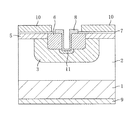
図1に示すように、この二重注入型MISFETは、濃度が1×1018cm-3以上のn型不純物(ドーパント)を含む低抵抗のSiC基板1と、SiC基板1の主面上に設けられ、濃度が1×1015cm-3〜1×1016cm-3程度のn型不純物がドープされている高抵抗SiC層2と、高抵抗SiC層2の表面部の一部に濃度が1×1016cm-3から1×1018cm-3のp型不純物をドープして形成されたpウェル領域3と、pウェル領域3の一部に濃度が約1×1019cm-3のn型不純物をドープして形成されたソース領域6と、ソース領域の直下方に位置するpウェル領域3の一部に高濃度のp型不純物をドープして形成されたp+コンタクト領域11と、pウェル領域3及び高抵抗SiC層2に跨って形成された積層ドープ層構造を含むチャネル層5と、チャネル層5の表面上に設けられた熱酸化膜からなる,V族元素含有酸化物層であるゲート絶縁膜7と、ゲート絶縁膜7の上に設けられたAl合金膜からなるゲート電極10と、ソース領域6を貫通してp+コンタクト領域11に到達する溝の壁面上に設けられ、p+コンタクト領域11及びソース領域7に接触するように設けられたソース電極8と、SiC基板1の裏面上にオーミック接触するように形成されたドレイン電極9とを備えている。
As shown in FIG. 1, this double-implant MISFET has a low-
各々n型半導体層であるソース領域6と高抵抗SiC層2とは、N型半導体層であるチャネル層5を介して電気的に接続された状態となっている。また、チャネル層5のうち、ソース領域上方に位置する部分の一部は除去されている。ソース電極8とソース領域6およびp+コンタクト領域11とは、互いにオーミック接触するように熱処理されている。SiC基板1とドレイン電極9とは互いにオーミック接触している。
Each of the
図2(a)〜(e)及び図3(a)〜(e)は、第1の実施形態のMISFETの製造工程を示す断面図である。 FIGS. 2A to 2E and FIGS. 3A to 3E are cross-sectional views showing manufacturing steps of the MISFET of the first embodiment.
まず、図2(a)に示す工程で、低抵抗のSiC基板1上に、SiC基板1より高抵抗の(ドーパント濃度が低い)高抵抗SiC層2をエピタキシャル成長させる。
First, in the step shown in FIG. 2A, a high
次に、図2(b)に示す工程で、例えばTEOS膜を堆積し、高抵抗SiC層2の上に、厚さ3μmの二酸化珪素膜21xを堆積する。その後、フォトリソグラフィーを行なって、二酸化珪素膜21xの上に、Pウェル形成領域が開口されたレジストマスクRe1を形成する。
Next, in the step shown in FIG. 2B, for example, a TEOS film is deposited, and a
次に、図2(c)に示す工程で、レジストマスクRe1をエッチングマスクとして用いたドライエッチングにより、二酸化珪素膜21xをパターニングして、二酸化珪素マスク21(イオン注入マスク)を形成する。そして、レジストマスクRe1を除去した後、二酸化珪素マスク21を用いて、基板を500℃以上の高温に保持した状態で、高抵抗SiC層2の表面部の一部にp型不純物のイオン注入を行なって、pウェル領域3を形成する。pウェル領域3におけるp型不純物の濃度は、通常1×1017cm-3前後から1×1018cm-3であり、pウェル領域3の深さはピンチオフしないように1μm前後とする。
Next, in the step shown in FIG. 2C, the
次に、図2(d)に示す工程で、二酸化珪素マスク21を除去し、注入された不純物を活性化するためのアニールを行なった後、pウェル領域3及び高抵抗SiC層2の表面上に、n型不純物を含むチャネル層5をエピタキシャル成長させる。
Next, in the step shown in FIG. 2 (d), the
次に、図2(e)に示す工程で、例えばTEOS膜を堆積し、チャネル層5の上に、厚さ3μmの二酸化珪素膜24xを堆積する。その後、フォトリソグラフィーを行なって、二酸化珪素膜24xの上に、ソース形成領域が開口されたレジストマスクRe2を形成する。
Next, in the step shown in FIG. 2E, for example, a TEOS film is deposited, and a
次に、図3(a)に示す工程で、レジストマスクRe2をエッチングマスクとして用いたドライエッチングにより、二酸化珪素膜24xをパターニングして、二酸化珪素マスク24(イオン注入マスク)を形成する。そして、レジストマスクRe2を除去した後、二酸化珪素マスク24を用いて、基板を500℃以上の高温に保持した状態で、チャネル層5及びpウェル領域3の一部に高濃度のn型不純物のイオン注入を行なうことにより、チャネル層5を貫通して、pウェル領域3の内部まで達するソース領域6を形成する。このとき、各々n型半導体層であるソース領域6と高抵抗SiC層2とは、n型半導体層であるチャネル層5を介して電気的に接続された状態となっている。
Next, in the step shown in FIG. 3A, the
次に、図3(b)に示す工程で、高濃度のp型不純物のイオン注入を行なって、ソース領域6の直下方に位置するpウェル領域3の一部にp+コンタクト領域11を形成する。そして、二酸化珪素マスク24を除去した後、p+コンタクト領域11やソース領域6に注入された不純物を活性化するためのアニールを行なう。さらに、ソース領域6を貫通してp+コンタクト領域11の上部に到達する溝4を形成した後、チャネル層5,ソース領域6及びp+コンタクト領域11の露出している表面部を熱酸化して、熱酸化膜を形成する。このとき、熱酸化膜は1200℃以上のドライ雰囲気中で形成され、その膜厚は40nm〜80nmである。これにより、炭化珪素−酸化物積層体Aが形成されることになる。さらに、熱酸化膜をV族元素含有ガスであるNOガス中でアニールして、窒化処理を行うことにより、熱酸化膜中にV族元素である窒素を導入して、V族元素含有酸化物層であるゲート絶縁膜7を形成する。このとき、窒化処理の温度は、1050℃〜1250℃の範囲内であり、処理圧力は6.67×10³Pa〜5.33×10⁴Paの範囲内である。
Next, in the step shown in FIG. 3B, ion implantation of high-concentration p-type impurities is performed to form a p + contact region 11 in a part of the p-
次に、図3(c)に示す工程で、ゲート絶縁膜7のうち溝4の壁面上の部分と、溝4の周囲の部分とを除去する。その後、さらに、ゲート絶縁膜7の除去により露出したソース領域6及びp+コンタクト領域11を深さ300nm程度までウエットエッチングして、界面準位密度の高い領域を除去する。
Next, in the step shown in FIG. 3C, the portion of the
次に、図3(d)に示す工程で、ソース領域6のうちゲート絶縁膜7が除去されて露出している部分の上にソース電極8を形成する。また、SiC基板1の裏面上にドレイン電極9を形成する。
Next, in the step shown in FIG. 3D, the
次に、図3(e)に示す工程で、ゲート絶縁膜7の上にゲート電極10を形成する。なお、ソース電極8とソース領域7及びp+コンタクト領域11とがオーミック接触し、SiC基板1とドレイン電極9とがオーミック接触するように熱処理が行われる。
Next, the
ここで、上記製造工程におけるNOアニール工程である,図3(b)に示す工程について説明する。 Here, the process shown in FIG. 3B, which is a NO annealing process in the manufacturing process, will be described.
図4(a)〜(b)は、第1の実施形態におけるV族元素含有酸化物層(ゲート絶縁膜7)を形成する手順を示す断面図である。図4(a)〜(b)においては、炭化珪素−酸化物積層体を模式的に表している。本実施形態においては、V族元素として、窒素を用いるが、リン(P),砒素(As)等の他のV族元素を用いてもよい。 FIGS. 4A and 4B are cross-sectional views illustrating a procedure for forming the V group element-containing oxide layer (gate insulating film 7) in the first embodiment. 4A to 4B schematically show a silicon carbide-oxide stack. In this embodiment, nitrogen is used as the group V element, but other group V elements such as phosphorus (P) and arsenic (As) may be used.
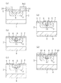
図4(a)に示す工程で、熱酸化膜であるゲート絶縁膜7’が表面上に形成された炭化珪素−酸化物積層体Aを、チャンバ20内に設置して、不活性ガス(Ar,N2,He,Ne等)雰囲気中で、1000℃以上の温度(例えば、1000℃〜1300℃)でアニールする。このアニール処理によって、熱酸化膜であるゲート絶縁膜7’が前もって緻密化される。この状態では、ゲート絶縁膜7’は、V族元素の導入処理が行われていない状態である。
In the step shown in FIG. 4A, a silicon carbide-oxide stack A having a
次に、図4(b)に示す工程で、炭化珪素−酸化物積層体Aを、除外装置(図示せず)及び減圧装置である真空ポンプ31が付設されたチャンバ30内に移動させて、チャンバ30内を真空ポンプ31によって約150Torr(2.0×10⁴Pa)に減圧しつつ、チャンバ30内に流量500(ml/min)のNOガス(又は、リン(P)などの窒素以外のV族元素含有ガス)を流し、チャンバ30内を窒素(N)(又は窒素以外のV族元素)がゲート絶縁膜7’中に拡散するのに十分に高い温度(例えば約1150℃)に加熱する。このとき、減圧下で、ゲート絶縁膜7’を窒素などのV族元素含有ガスに暴露することにより、ゲート絶縁膜7内に窒素などのV族元素が拡散し、比誘電率の大きい,より緻密なV族元素含有酸化物層であるゲート絶縁膜7が形成される。暴露は、緻密なV族元素含有酸化物層を形成するのに充分な、そして、ゲート絶縁膜7(V族元素含有酸化物層)の特性が改良となるのに充分な時間(例えば1Hr)の間行なう。
Next, in the step shown in FIG. 4B, the silicon carbide-oxide stack A is moved into a
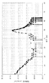
図5は、本実施形態の製造方法によって形成されたV族元素含有酸化物層であるゲート絶縁膜7の厚さ方向における窒素濃度をSIMSにより実測した窒素濃度プロファイルを示すデータである。同図に示すデータでは、ゲート絶縁膜7(V族元素含有酸化物層)の厚さが約50nmである。同図に示されるように、NOガスへの暴露処理によって、ゲート絶縁膜7(V族元素含有酸化物層)中には窒素が拡散しており、特に、ゲート絶縁膜7(V族元素含有酸化物層)のうち下地のSiC層(ソース領域6又はP+コンタクト領域11)に近い領域において窒素濃度が6×10²⁰atoms/103という、鋭いピーク部が現れている。そして、ピーク部の厚さ方向の寸法は、半値幅で3nmである。そして、このゲート絶縁膜7(V族元素含有酸化物層)全体の比誘電率は約3.3である。
FIG. 5 is data showing a nitrogen concentration profile in which the nitrogen concentration in the thickness direction of the
図6は、図5に示すデータを採取したサンプルとは異なるサンプルであってV族含有酸化物層の厚みを厚くしたサンプルにおける窒素濃度のピーク部(SiO2−SiC界面付近の領域)の濃度分布を抜き出して示す図である。同図に示すデータは、SiO2−SiC界面での窒素をCsN147で定量して得られたものである。 FIG. 6 shows the concentration of the nitrogen concentration peak (region near the SiO 2 -SiC interface) in a sample different from the sample from which the data shown in FIG. 5 was collected and in which the thickness of the V group-containing oxide layer was increased. It is a figure which extracts and shows distribution. The data shown in the figure is obtained by quantifying nitrogen at the SiO 2 -SiC interface with CsN 147 .
同図に示すように、このピーク部の半値幅は3nmであり、非常に狭い領域に窒素が集中的に高濃度で導入されていることがわかる。ピーク部の半値幅は、5nm以下であることが好ましい。 As shown in the figure, the half-value width of this peak portion is 3 nm, and it can be seen that nitrogen is intensively introduced at a high concentration in a very narrow region. The full width at half maximum of the peak portion is preferably 5 nm or less.
このように、酸化物層に窒素,リン(P)などのV族元素を導入することにより、高い比誘電率を有するV族元素含有酸化物層を形成することができる。そして、本実施形態のV族元素含有酸化物層であるゲート絶縁膜7を有するMISFETによると、ゲートバイアスを下地層に効率よく作用させることができ、高い電流駆動力を実現することができる。
Thus, by introducing a group V element such as nitrogen or phosphorus (P) into the oxide layer, a group V element-containing oxide layer having a high relative dielectric constant can be formed. And according to the MISFET having the
なお、V族元素含有酸化物層を容量絶縁膜とするMISキャパシタを構成した場合にも、SiC基板上に比誘電率の高いMISキャパシタが形成されることになる。 Even when a MIS capacitor using a group V element-containing oxide layer as a capacitive insulating film is formed, a MIS capacitor having a high relative dielectric constant is formed on the SiC substrate.
図7は、本実施形態の方法により形成したゲート絶縁膜7(V族元素含有酸化物層)を容量絶縁膜として備えたMISキャパシタ(ゲート電極10,ゲート絶縁膜7及びチャネル層5によって構成されるキャパシタ)のCV測定の結果を示す図である。同図の横軸は電極間の電圧を表し、同図の縦軸は容量を表している。このサンプルは、V族元素含有酸化物層であるゲート絶縁膜7の上にキャパシタの上部電極であるゲート電極10を形成する際に、950℃以上の熱処理を経ている。同図におけるQuasi-static CV曲線と、高周波(1MHz)で測定したCV曲線とを比較すると、両者の差がわずかであることから界面準位密度が減少していることがわかる。
FIG. 7 shows a MIS capacitor (
図8(a)〜(b)は、図6に示すデータに基づいて、High-Low法で計算した界面準位密度を示す図である。図8(a)〜(b)において、横軸は価電子帯(ヴァレンスバンド)Evとのポテンシャル差(E−Ev(eV))を表し、縦軸は界面準位密度Dit(cm-2eV-1)を表している。キャリアが電子である場合(Nチャネル型MISFET)には、トラップとして作用する界面準位はコンダクションバンド端付近のポテンシャル範囲(E−Ev=2.95eV〜3.05eV)の界面準位であり、キャリアがホールである場合(Pチャネル型MISFET)には、ホールトラップとして作用する界面準位はヴァレンスバンド端付近のポテンシャル範囲(E−Ev=0.3eV〜0.4eV)の界面準位であるが、図8(a)〜(b)に示すように、本実施形態においては、各バンド端付近のポテンシャル範囲において1×1012cm-2・eV-1以下の界面状態密度が得られている。また、ゲート絶縁膜7(V族元素含有酸化物層)全体における窒素の平均濃度は、8.3×1019cm-3である。 FIGS. 8A to 8B are diagrams showing the interface state density calculated by the High-Low method based on the data shown in FIG. 8A and 8B, the horizontal axis represents the potential difference (E-Ev (eV)) from the valence band Ev, and the vertical axis represents the interface state density Dit (cm −2 eV). -1 ). When the carrier is an electron (N-channel MISFET), the interface state acting as a trap is an interface state in the potential range (E-Ev = 2.95 eV to 3.05 eV) near the end of the conduction band. When the carrier is a hole (P channel type MISFET), the interface state acting as a hole trap is the interface state in the potential range (E-Ev = 0.3 eV to 0.4 eV) near the edge of the valence band. However, as shown in FIGS. 8A to 8B, in this embodiment, an interface state density of 1 × 10 12 cm −2 · eV −1 or less is obtained in the potential range near each band edge. ing. The average concentration of nitrogen in the entire gate insulating film 7 (group V element-containing oxide layer) is 8.3 × 10 19 cm −3 .
このように、V族元素含有酸化物層を容量絶縁膜とするMISキャパシタを構成した場合、容量絶縁膜と、下部電極であるSiC層との間の界面付近の領域における界面準位密度を低減することができることがわかる。 Thus, when a MIS capacitor having a group V element-containing oxide layer as a capacitive insulating film is configured, the interface state density in the region near the interface between the capacitive insulating film and the SiC layer as the lower electrode is reduced. You can see that you can.
したがって、MISキャパシタを利用してMISFETを形成した場合にも、キャリアのトラップとなる界面準位密度の低減により、キャリア移動度の向上を図ることができる。 Therefore, even when a MISFET is formed using a MIS capacitor, the carrier mobility can be improved by reducing the interface state density that becomes a carrier trap.
特に、V族元素含有酸化物層であるゲート絶縁膜7の下部における窒素濃度の最大値が、1×1020cm-3以上で、1×1022cm-3以下であることにより、比誘電率の向上作用と、界面準位密度の低減作用とが顕著に得られる。
In particular, the maximum value of the nitrogen concentration in the lower portion of the
−図4(b)に示す工程における好ましい条件−
図4(b)において使用される窒素を含むガスとしては、例えば、NOガス,N2Oガス,NO2ガス,PH3ガスなどがあり、特に、NOガス又はN2Oガスを用いることによる効果が大きい。つまり、窒素を含むガスとして現実に最適なガスは、NOガス,N2Oガスであり、これらは酸素を含むガスでもある。その場合には、下地のSiC層の酸化を抑制する観点から、以下のような条件が好ましい。
-Preferred conditions in the step shown in Fig. 4 (b)-
Examples of the gas containing nitrogen used in FIG. 4B include NO gas, N 2 O gas, NO 2 gas, PH 3 gas, and the like, and particularly by using NO gas or N 2 O gas. Great effect. That is, the gas that is actually optimal as the gas containing nitrogen is NO gas and N 2 O gas, and these are also gases containing oxygen. In that case, the following conditions are preferable from the viewpoint of suppressing oxidation of the underlying SiC layer.
[圧力条件]
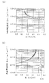
図9は、第1の実施形態のMISFETのチャネル移動度のNOアニールにおける圧力依存性を示す図である。同図は、温度を1050℃から1150℃の間で変化させてアニール処理を行なったサンプルについてのデータをグラフにしたものである。また、チャネル移動度は、ゲートバイアスが5V〜20Vでもっとも高くなるので、その付近でのデータである。
[Pressure conditions]
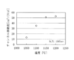
FIG. 9 is a diagram showing the pressure dependence of the channel mobility of the MISFET of the first embodiment in NO annealing. This figure is a graph of data on a sample that was annealed by changing the temperature between 1050 ° C. and 1150 ° C. FIG. Further, the channel mobility is the highest when the gate bias is 5 V to 20 V, and is data in the vicinity thereof.
同図に示すように、50Torr〜400Torr(6.67×10³Pa〜5.33×10⁴Pa))の範囲(好適範囲)で高いチャネル移動度が得られている。そして、ピーク位置は、約150Torr(2.0×10⁴Pa)その理由について、以下に説明する。 As shown in the figure, high channel mobility is obtained in a range (preferable range) of 50 Torr to 400 Torr (6.67 × 10 3 Pa to 5.33 × 10 4 Pa)). The reason why the peak position is about 150 Torr (2.0 × 10 4 Pa) will be described below.
図4(b)に示す工程におけるSiC層の熱酸化の際、又は、酸化物の蒸着の際には、通常、単結晶SiC基板もしくはエピレイヤー(epilayer)(エピタキシャル成長されたSiC層)が、その珪素面(silicon face)と炭素面(carbon face)に沿って、あるいはこれらの面に垂直なA軸(例えば[ 1 1 2 0]方向,または[ 1 1 0 0]方向)の1つに沿って供給される。炭素(C)は珪素(Si)より幾らか容易に酸化され(従って、他の全てのファクターが実質的に等しければ酸化がより速い)、炭素面上の酸化は900℃〜1300℃の温度で進行し、珪素面上の酸化は約1000℃〜1400℃の温度で進行する。 When the SiC layer is thermally oxidized in the step shown in FIG. 4B or when the oxide is deposited, a single crystal SiC substrate or an epilayer (epitaxially grown SiC layer) is usually used. Along the silicon face and carbon face, or along one of the A axes perpendicular to these faces (eg, [1 1 2 0] direction or [1 1 0 0] direction) Supplied. Carbon (C) oxidizes somewhat more easily than silicon (Si) (and therefore is faster if all other factors are substantially equal), and oxidation on the carbon surface occurs at temperatures between 900 ° C and 1300 ° C. The oxidation on the silicon surface proceeds at a temperature of about 1000 ° C. to 1400 ° C.
したがって、図4(b)に示す工程で、窒素を含むガスとして酸素をも含むガスを用いる場合にも、炭素面上の酸化は、900℃〜1300℃の温度で進行し、珪素面上の酸化は、1000℃〜1400℃の温度で進行することになる。窒素以外のV族元素を含むガスを用いた場合も同様である。 Therefore, in the step shown in FIG. 4B, even when a gas containing oxygen is used as the gas containing nitrogen, the oxidation on the carbon surface proceeds at a temperature of 900 ° C. to 1300 ° C., and on the silicon surface. Oxidation proceeds at a temperature of 1000 ° C to 1400 ° C. The same applies when a gas containing a group V element other than nitrogen is used.
以上のように、酸素を含む雰囲気下では、一般に、900℃以上の温度でSiCの熱酸化が生じることが観測されている。ところが、900℃以上の高温下であっても、減圧下では、炭素面上及び珪素面上において、共に酸化が抑制される。特に、400Torr(5.33×10⁴Pa)以下の圧力下では、酸化が進行しチャネル移動度の改善効果が低下する。特に、本実施形態におけるNOガスのように、窒素を含むガスとして酸素を含むガスでもあるガスを用いて酸化物層(ゲート絶縁膜7’)をアニール処理する場合には、減圧下、特に400Torr(5.33×10⁴Pa)以下の圧力下で行なうことが好ましい。ただし、あまりに低い減圧雰囲気下においては、酸化物層(ゲート絶縁膜7’)内への窒素の拡散が抑制されるので、50Torr(6.67×10³Pa)以上の圧力下で行なうことが好ましい。よって、図4(b)に示す,酸化物層を窒素を含むガスに暴露する処理は、6.67×10³Pa以上で5.33×10⁴Pa以下の範囲の圧力下で行なうことが好ましい。
As described above, in an atmosphere containing oxygen, it is generally observed that SiC is thermally oxidized at a temperature of 900 ° C. or higher. However, even at a high temperature of 900 ° C. or higher, oxidation is suppressed on both the carbon surface and the silicon surface under reduced pressure. In particular, under a pressure of 400 Torr (5.33 × 10 4 Pa) or less, oxidation proceeds and the effect of improving channel mobility decreases. In particular, when the oxide layer (
ただし、不活性ガス(ArやN2ガス)をも流してて雰囲気全体の圧力が大気圧ないし大気圧に近い減圧雰囲気であっても、V元素含有ガスの分圧が6.67×10³Pa以上で5.33×10⁴Pa以下の範囲であれば、同様の効果を発揮することは可能である。 However, the partial pressure of the V element-containing gas is 6.67 × 10 3 even in a reduced-pressure atmosphere in which an inert gas (Ar or N 2 gas) is also flowed and the pressure of the whole atmosphere is at or near atmospheric pressure. The same effect can be exhibited if it is in the range of Pa to 5.33 × 10 4 Pa or less.
[温度条件]
図10は、第1の実施形態のMISFETのチャネル移動度のNOアニール温度依存性を示す図である。同図のデータは、アニール時間が1時間,圧力が150Torr(2.00×10⁴Pa)の条件でアニール処理を行なったサンプルについてのものである。同図に示すように、1100℃を超え1250℃未満の範囲、より好ましくは、1150℃以上で1200℃以下の範囲で、比較的高いチャネル移動度が得られている。その理由について、以下に説明する。
[Temperature conditions]
FIG. 10 is a diagram showing the NO annealing temperature dependence of the channel mobility of the MISFET of the first embodiment. The data in this figure is for a sample that was annealed under conditions of an annealing time of 1 hour and a pressure of 150 Torr (2.00 × 10 4 Pa). As shown in the figure, a relatively high channel mobility is obtained in the range of more than 1100 ° C. and less than 1250 ° C., more preferably in the range of 1150 ° C. to 1200 ° C. The reason will be described below.
一般に、1100℃を超える温度で窒素を含むガスへの暴露処理を行なうと、窒素が酸化物層(ゲート絶縁膜7’)内に速やかに拡散することがわかっている。ただし、酸素の酸化物層内への拡散を抑制するためには、1250℃以下の温度であることが好ましい。
In general, it is known that when an exposure treatment to a gas containing nitrogen is performed at a temperature exceeding 1100 ° C., nitrogen is quickly diffused into the oxide layer (
図11は、第1の実施形態のMISFETの界面準位密度のNOアニール温度依存性を示す図である。同図のデータは、アニール時間が1時間,圧力が150Torr(2.00×10⁴Pa)の条件でアニール処理を行なったサンプルについて、ポテンシャル位置(E−Ev)が3.0eVにおける界面準位密度を示している。同図に示すように、1100℃を超え1250℃未満の範囲、より好ましくは、1150℃以上で1200℃以下の範囲で、界面準位密度が非常に小さくなっており、これによって、高いチャネル移動度が得られることがわかる。 FIG. 11 is a diagram showing the NO annealing temperature dependence of the interface state density of the MISFET of the first embodiment. The data in the figure shows the interface state at the potential position (E-Ev) of 3.0 eV for the sample annealed under the conditions of an annealing time of 1 hour and a pressure of 150 Torr (2.00 × 10 4 Pa). The density is shown. As shown in the figure, the interface state density is very small in the range of more than 1100 ° C. and less than 1250 ° C., more preferably in the range of 1150 ° C. to 1200 ° C. It can be seen that the degree is obtained.
したがって、図4(b)に示す工程における好ましい温度範囲は、1100℃〜1250℃であり、より好ましくは、1150℃〜1200℃である。窒素以外のV族元素,例えばリン(P)を用いる場合も同様である。 Therefore, a preferable temperature range in the step shown in FIG. 4B is 1100 ° C. to 1250 ° C., and more preferably 1150 ° C. to 1200 ° C. The same applies when using a group V element other than nitrogen, such as phosphorus (P).
さらに、一般的には、1300℃以下において、酸化物層の表面荒れが起こりにくくなる。 Furthermore, generally, the surface roughness of the oxide layer hardly occurs at 1300 ° C. or lower.
上記実施形態では、SiC層(チャネル層5,ソース領域6及びP+コンタクト領域11)上の酸化物層(ゲート絶縁膜7’)を熱酸化することによって形成したが、酸化物層を必ずしも熱酸化法によって形成する必要はない。他の方法[例えば、シランバス(SiH4)と酸素(O2)を用いた低圧化学蒸着法(LPCVD),プラズマ蒸着法による酸化物層の形成や、CVD法,蒸着法,熱酸化法のあらゆる組み合わせ]を用いて、SiC層上に酸化物層を堆積させることもできる。
In the above embodiment, the oxide layer (
なお、本実施形態では、蓄積型MISFETについて説明したが、蓄積型MISFETのチャネル移動度によって界面準位密度そのものを評価するためにすぎない。したがって、反転型MISFETにおいても、本実施形態の条件によって高いチャネル移動度が得られることがわかる。 Although the storage type MISFET has been described in the present embodiment, it is merely for evaluating the interface state density itself based on the channel mobility of the storage type MISFET. Therefore, it can be seen that a high channel mobility can be obtained also in the inverting MISFET according to the conditions of the present embodiment.
(第2の実施形態)
本実施形態においては、炭化珪素−酸化物積層体の構造は、第1の実施形態と基本的は同じであるので、説明を省略し、製造工程のみについて説明する。
(Second Embodiment)
In the present embodiment, the structure of the silicon carbide-oxide stacked body is basically the same as that of the first embodiment, and thus description thereof will be omitted and only the manufacturing process will be described.
本実施形態においては、図4(b)に示す工程の前に、SiC層の表面上に第1の酸化物層を形成する。このとき、第1の酸化物層の厚さは、20nm未満,例えば8nm程度であることが好ましい。その後、不活性ガス(Ar,N2,He,Ne等)雰囲気中で、1000℃以上の温度(例えば、1000℃〜1150℃)でアニールする。このアニール処理によって、第1の酸化物層が前もって緻密化される。 In the present embodiment, a first oxide layer is formed on the surface of the SiC layer before the step shown in FIG. At this time, the thickness of the first oxide layer is preferably less than 20 nm, for example, about 8 nm. Thereafter, annealing is performed at a temperature of 1000 ° C. or higher (eg, 1000 ° C. to 1150 ° C.) in an inert gas (Ar, N 2 , He, Ne, etc.) atmosphere. By this annealing treatment, the first oxide layer is densified in advance.
次に、NOガス,N2Oガスなどの窒素を含むガス、又はリン(P)を含むガスに、例えば1150℃,チャンバ内圧力が150Torr(約2.00×10⁴Pa)の条件で、1時間の間、アニールを行なう。 Next, in a gas containing nitrogen such as NO gas, N 2 O gas, or a gas containing phosphorus (P), for example, under the conditions of 1150 ° C. and the pressure in the chamber being 150 Torr (about 2.00 × 10 4 Pa), Annealing is performed for 1 hour.
次に、約300℃の温度でのECR−pCVDにより、第1の酸化物層の上に、厚さが例えば75nm程度の第2の酸化物層(例えば、SiO2,SiN,HfO2などの高誘電体膜)を形成する。 Next, by ECR-pCVD at a temperature of about 300 ° C., a second oxide layer (for example, SiO 2 , SiN, HfO 2, etc.) having a thickness of about 75 nm is formed on the first oxide layer. High dielectric film).
その後、900℃以上1100℃以下の温度で(例えば1000℃)、不活性ガス雰囲気(例えばAr雰囲気)中で、1時間程度のアニールを行なう。 Thereafter, annealing is performed at a temperature of 900 ° C. to 1100 ° C. (eg, 1000 ° C.) in an inert gas atmosphere (eg, Ar atmosphere) for about 1 hour.
図12は、第2の実施形態の方法により形成したV族元素含有酸化物層を容量絶縁膜として備えたMISキャパシタのCV測定の結果を示す図である。同図の横軸は電極間の電圧を表し、同図の縦軸は容量を表している。同図における実験曲線と、理論曲線とを比較すると、両者の差がわずかであることから界面準位密度が減少していることがわかる。 FIG. 12 is a diagram showing a result of CV measurement of a MIS capacitor provided with a group V element-containing oxide layer formed by the method of the second embodiment as a capacitive insulating film. The horizontal axis of the figure represents the voltage between the electrodes, and the vertical axis of the figure represents the capacitance. Comparing the experimental curve and the theoretical curve in the figure, it can be seen that the interface state density is reduced because the difference between the two is small.
したがって、第2の実施形態の方法によっても、第1,第2の酸化物層からなるV族元素含有酸化物層によって、界面準位密度の低減により、第1の実施形態と同様の効果を発揮することができる。 Therefore, also by the method of the second embodiment, the same effect as that of the first embodiment can be obtained by reducing the interface state density by the V group element-containing oxide layer composed of the first and second oxide layers. It can be demonstrated.
また、本実施形態の製造方法によると、40nmを越える厚さのV族元素含有酸化物層を形成する場合にも、高品質の炭化珪素−酸化物積層体が得られることになる。 In addition, according to the manufacturing method of the present embodiment, a high-quality silicon carbide-oxide stack can be obtained even when a V-group element-containing oxide layer having a thickness exceeding 40 nm is formed.
本発明の炭化珪素−酸化物積層体及びその製造方法は、縦型,横型のMISFET型パワーデバイスや、MISキャパシタの製造に利用することができる。 The silicon carbide-oxide laminate of the present invention and the manufacturing method thereof can be used for manufacturing vertical and horizontal MISFET power devices and MIS capacitors.
10 SiC基板
11 酸化物層
12 V族元素含有酸化物層
20 チャンバ
30 チャンバ
31 真空ポンプ
10
Claims (17)
上記炭化珪素層の上に形成され、少なくとも下部にV族元素濃度の高い領域を有し、かつ、比誘電率が3.0以上であるV族元素含有酸化物層と
を備えている炭化珪素−酸化物積層体。 A silicon carbide layer;
Silicon carbide formed on the silicon carbide layer and having a group V element-containing oxide layer having at least a region having a high group V element concentration and a relative dielectric constant of 3.0 or more An oxide laminate.
上記V族元素含有酸化物層の下部におけるV族元素濃度分布中のピーク部の半値幅が5nm以下である,炭化珪素−酸化物積層体。 In the silicon carbide-oxide laminate according to claim 1,
A silicon carbide-oxide stacked body, wherein a half value width of a peak portion in a V group element concentration distribution at a lower portion of the V group element-containing oxide layer is 5 nm or less.
上記V族元素含有酸化物層は、母材がSiO2によって構成されている,炭化珪素−酸化物積層体。 In the silicon carbide-oxide laminate according to claim 1 or 2,
The group V element-containing oxide layer is a silicon carbide-oxide stack in which a base material is composed of SiO 2 .
上記V族元素は窒素又は燐であり、
上記V族元素含有酸化物層の下部におけるV族元素濃度の最大値が、1×1020cm-3以上で1×1022cm-3以下である,炭化珪素−酸化物積層体。 In the silicon carbide-oxide laminate according to any one of claims 1 to 3,
The group V element is nitrogen or phosphorus,
A silicon carbide-oxide stack in which the maximum value of the group V element concentration in the lower portion of the group V element-containing oxide layer is 1 × 10 20 cm −3 or more and 1 × 10 22 cm −3 or less.
上記V族元素含有酸化物層の上記炭化珪素層との境界付近の領域における界面準位密度は、伝導帯及び価電子帯のうち少なくともいずれかのバンド端付近のポテンシャル範囲で1×1012cm-3/eV以下である,炭化珪素−酸化物積層体。 In the silicon carbide-oxide laminate according to any one of claims 1 to 4,
The interface state density in the region near the boundary between the V group element-containing oxide layer and the silicon carbide layer is 1 × 10 12 cm in the potential range near the band edge of at least one of the conduction band and the valence band. -3 / eV or less, a silicon carbide-oxide laminate.
上記炭化珪素層は、
ソース領域又はドレイン領域のうち少なくともいずれか一方として機能する第1導電型の不純物拡散領域と、
上記不純物拡散領域の側方に位置するチャネル領域と、
上記不純物拡散領域を挟んで上記チャネル領域とは対向する位置に設けられ、表面部がエッチングにより除去された第2導電型コンタクト領域とを含み、
上記V族元素含有酸化物層は、上記チャネル領域の上に設けられたゲート酸化膜を含む,半導体装置。 A silicon carbide layer, a V group element-containing oxide layer formed on the silicon carbide layer and having a region having a high V group element concentration at least below, and at least a part of the V group element containing oxide layer A semiconductor device comprising a gate electrode provided in
The silicon carbide layer is
A first conductivity type impurity diffusion region functioning as at least one of a source region and a drain region;
A channel region located on the side of the impurity diffusion region;
A second conductivity type contact region provided at a position facing the channel region across the impurity diffusion region and having a surface portion removed by etching;
The group V element-containing oxide layer includes a gate oxide film provided on the channel region.
上記工程(a)の後に、上記炭化珪素層をチャンバ内に設置して、上記酸化物層を、1100℃よりも高く1250℃よりも低い温度範囲で、V族元素含有ガスを含む雰囲気に曝露して、上記酸化物層を比誘電率が3.0以上のV族元素含有酸化物層に変化させる工程(b)と
を含む炭化珪素−酸化物積層体の製造方法。 Forming an oxide layer on the surface of the silicon carbide layer (a);
After the step (a), the silicon carbide layer is placed in a chamber, and the oxide layer is exposed to an atmosphere containing a group V element-containing gas in a temperature range higher than 1100 ° C. and lower than 1250 ° C. And a step (b) of changing the oxide layer into a V group element-containing oxide layer having a relative dielectric constant of 3.0 or more.
上記工程(b)は、6.67×10³Pa以上で5.33×10⁴Pa以下の範囲に減圧された雰囲気で行なわれる,炭化珪素−酸化物積層体の製造方法。 In the manufacturing method of the silicon carbide-oxide laminated body of Claim 7,
The said process (b) is a manufacturing method of the silicon carbide-oxide laminated body performed in the atmosphere pressure-reduced to the range of 6.67 * 10 < 3 > Pa or more and 5.33 * 10 < 4 > Pa or less.
上記工程(b)は、上記V族元素含有ガスを含む雰囲気の圧力は大気圧で、上記V族元素含有ガスの分圧が6.67×10³Pa以上で5.33×10⁴Pa以下の範囲である雰囲気で行なわれる,炭化珪素−酸化物積層体の製造方法。 In the manufacturing method of the silicon carbide-oxide laminated body of Claim 7 or 8,
In the step (b), the pressure of the atmosphere containing the group V element-containing gas is atmospheric pressure, and the partial pressure of the group V element-containing gas is 6.67 × 10 3 Pa or more and 5.33 × 10 4 Pa or less. A method for producing a silicon carbide-oxide laminate, which is performed in an atmosphere in a range of
上記工程(a)では、熱酸化により酸化物層を形成した後、不活性ガス雰囲気中でアニールする処理を行う,炭化珪素−酸化物積層体の製造方法。 In the manufacturing method of the silicon carbide-oxide laminated body as described in any one of Claims 7-9,
In the step (a), the oxide layer is formed by thermal oxidation, and then annealing is performed in an inert gas atmosphere.
上記工程(a)では、上記不活性ガス雰囲気中でアニールした後、850℃以上で950℃以下の温度で、酸化性ガス雰囲気中で酸化する処理をさらに行う,炭化珪素−酸化物積層体の製造方法。 In the manufacturing method of the silicon carbide-oxide laminated body of Claim 10,
In the step (a), after annealing in the inert gas atmosphere, a process of further oxidizing in an oxidizing gas atmosphere at a temperature of 850 ° C. or higher and 950 ° C. or lower is further performed. Production method.
上記V族元素含有ガスは、窒素又は燐を含んでいる,炭化珪素−酸化物積層体の製造方法。 In the manufacturing method of the silicon carbide-oxide laminated body as described in any one of Claims 7-11,
The said group V element containing gas is a manufacturing method of the silicon carbide-oxide laminated body in which nitrogen or phosphorus is included.
上記V族元素含有ガスとして、NOガス,N2Oガス,NO2ガス及びPH3ガスの中から選ばれる少なくとも1つのガスを用いる,炭化珪素−酸化物積層体の製造方法。 In the manufacturing method of the silicon carbide-oxide laminated body of Claim 12,
A method for producing a silicon carbide-oxide laminate, wherein at least one gas selected from NO gas, N 2 O gas, NO 2 gas, and PH 3 gas is used as the group V element-containing gas.
上記工程(a)の後に、上記炭化珪素層をチャンバ内に設置して、上記酸化物層をV族元素含有ガスを含むガス雰囲気に曝露する工程(b)と、
上記工程(b)の後に、上記第1の酸化物層の上に、第2の酸化物層を堆積する工程(c)と、
上記工程(c)の後に、900℃以上1100℃以下の温度で、不活性ガス雰囲気中でアニールすることにより、上記第1の酸化物層及び第2の酸化物層からなる酸化物層を比誘電率が3.0以上のV族元素含有酸化物層に変化させる工程(d)と
を含む炭化珪素−酸化物積層体の製造方法。 Forming a first oxide layer on the surface of the silicon carbide layer (a);
(B) after the step (a), placing the silicon carbide layer in a chamber and exposing the oxide layer to a gas atmosphere containing a group V element-containing gas;
(C) depositing a second oxide layer on the first oxide layer after the step (b);
After the step (c), the oxide layer composed of the first oxide layer and the second oxide layer is compared by annealing in an inert gas atmosphere at a temperature of 900 ° C. to 1100 ° C. And a step (d) of changing to a group V element-containing oxide layer having a dielectric constant of 3.0 or more.
上記工程(b)は、6.67×10³Pa以上で5.33×10⁴Pa以下の範囲に減圧された雰囲気で行なわれる,炭化珪素−酸化物積層体の製造方法。 In the manufacturing method of the silicon carbide-oxide laminated body of Claim 14,
The said process (b) is a manufacturing method of the silicon carbide-oxide laminated body performed in the atmosphere pressure-reduced to the range of 6.67 * 10 < 3 > Pa or more and 5.33 * 10 < 4 > Pa or less.
上記工程(a)では、厚さ20nm未満の熱酸化膜を形成する,炭化珪素−酸化物積層体の製造方法。 In the manufacturing method of the silicon carbide-oxide laminated body of Claim 14 or 15,
In the step (a), a method for producing a silicon carbide-oxide laminate, wherein a thermal oxide film having a thickness of less than 20 nm is formed.
上記工程(b)では、上記V族元素含有ガスとして、NOガス,N2Oガス,NO2ガス及びPH3ガスの中から選ばれる少なくとも1つのガスを用いる,炭化珪素−酸化物積層体の製造方法。 In the manufacturing method of the silicon carbide-oxide laminated body as described in any one of Claims 14-16,
In the step (b), at least one gas selected from NO gas, N 2 O gas, NO 2 gas, and PH 3 gas is used as the group V element-containing gas. Production method.
Priority Applications (1)
| Application Number | Priority Date | Filing Date | Title |
|---|---|---|---|
| JP2004271321A JP2005136386A (en) | 2003-10-09 | 2004-09-17 | Silicon carbide-oxide laminate, manufacturing method therefor, and semiconductor device |
Applications Claiming Priority (2)
| Application Number | Priority Date | Filing Date | Title |
|---|---|---|---|
| JP2003350244 | 2003-10-09 | ||
| JP2004271321A JP2005136386A (en) | 2003-10-09 | 2004-09-17 | Silicon carbide-oxide laminate, manufacturing method therefor, and semiconductor device |
Publications (2)
| Publication Number | Publication Date |
|---|---|
| JP2005136386A true JP2005136386A (en) | 2005-05-26 |
| JP2005136386A5 JP2005136386A5 (en) | 2005-12-15 |
Family
ID=34656036
Family Applications (1)
| Application Number | Title | Priority Date | Filing Date |
|---|---|---|---|
| JP2004271321A Withdrawn JP2005136386A (en) | 2003-10-09 | 2004-09-17 | Silicon carbide-oxide laminate, manufacturing method therefor, and semiconductor device |
Country Status (1)
| Country | Link |
|---|---|
| JP (1) | JP2005136386A (en) |
Cited By (17)
| Publication number | Priority date | Publication date | Assignee | Title |
|---|---|---|---|---|
| JPWO2007086196A1 (en) * | 2006-01-30 | 2009-06-18 | 住友電気工業株式会社 | Method for manufacturing silicon carbide semiconductor device |
| JP2010040564A (en) * | 2008-07-31 | 2010-02-18 | Sumitomo Electric Ind Ltd | Silicon carbide semiconductor device and manufacturing method thereof |
| JP2010171418A (en) * | 2008-12-25 | 2010-08-05 | Rohm Co Ltd | Semiconductor device and method of manufacturing semiconductor device |
| WO2011027540A1 (en) * | 2009-09-02 | 2011-03-10 | パナソニック株式会社 | Semiconductor element and method for manufacturing same |
| WO2011074237A1 (en) * | 2009-12-16 | 2011-06-23 | 国立大学法人奈良先端科学技術大学院大学 | Sic semiconductor element and manufacturing method for same |
| US20120199850A1 (en) * | 2010-01-19 | 2012-08-09 | Sumitomo Electric Industries, Ltd. | Silicon carbide semiconductor device and method of manufacturing thereof |
| DE112010001476T5 (en) | 2009-03-11 | 2012-09-20 | Mitsubishi Electric Corporation | Process for producing a silicon carbide semiconductor device |
| US20120248461A1 (en) * | 2011-04-01 | 2012-10-04 | Sumitomo Electric Industries, Ltd. | Silicon carbide semiconductor device |
| US8421151B2 (en) | 2009-10-22 | 2013-04-16 | Panasonic Corporation | Semiconductor device and process for production thereof |
| US8450750B2 (en) | 2010-01-27 | 2013-05-28 | Sumitomo Electric Industries, Ltd. | Silicon carbide semiconductor device and method of manufacturing thereof |
| JP2013149842A (en) * | 2012-01-20 | 2013-08-01 | Mitsubishi Electric Corp | Method of manufacturing silicon carbide semiconductor device |
| JP2015023043A (en) * | 2013-07-16 | 2015-02-02 | 三菱電機株式会社 | Method of manufacturing silicon carbide semiconductor device |
| EP2998984A1 (en) * | 2014-09-19 | 2016-03-23 | Kabushiki Kaisha Toshiba | Semiconductor device and method of manufacturing the same |
| JP2016063122A (en) * | 2014-09-19 | 2016-04-25 | 株式会社東芝 | Semiconductor device |
| JP2016154236A (en) * | 2008-12-25 | 2016-08-25 | ローム株式会社 | Semiconductor device |
| JP2016181671A (en) * | 2015-03-24 | 2016-10-13 | 株式会社東芝 | Semiconductor device, inverter circuit, driving device, vehicle and lift |
| JP2018129420A (en) * | 2017-02-09 | 2018-08-16 | 株式会社東芝 | Semiconductor device, manufacturing method thereof, inverter circuit, driving device, vehicle, and elevator |
-
2004
- 2004-09-17 JP JP2004271321A patent/JP2005136386A/en not_active Withdrawn
Cited By (39)
| Publication number | Priority date | Publication date | Assignee | Title |
|---|---|---|---|---|
| JPWO2007086196A1 (en) * | 2006-01-30 | 2009-06-18 | 住友電気工業株式会社 | Method for manufacturing silicon carbide semiconductor device |
| JP2010040564A (en) * | 2008-07-31 | 2010-02-18 | Sumitomo Electric Ind Ltd | Silicon carbide semiconductor device and manufacturing method thereof |
| JP7054403B2 (en) | 2008-12-25 | 2022-04-13 | ローム株式会社 | Manufacturing method of semiconductor device |
| US11152501B2 (en) | 2008-12-25 | 2021-10-19 | Rohm Co., Ltd. | Semiconductor device |
| US9837531B2 (en) | 2008-12-25 | 2017-12-05 | Rohm Co., Ltd. | Semiconductor device |
| JP7381643B2 (en) | 2008-12-25 | 2023-11-15 | ローム株式会社 | Manufacturing method of semiconductor device |
| US10693001B2 (en) | 2008-12-25 | 2020-06-23 | Rohm Co., Ltd. | Semiconductor device |
| US11804545B2 (en) | 2008-12-25 | 2023-10-31 | Rohm Co., Ltd. | Semiconductor device |
| JP2020145483A (en) * | 2008-12-25 | 2020-09-10 | ローム株式会社 | Manufacturing method of semiconductor device |
| JP2010171418A (en) * | 2008-12-25 | 2010-08-05 | Rohm Co Ltd | Semiconductor device and method of manufacturing semiconductor device |
| JP2016154236A (en) * | 2008-12-25 | 2016-08-25 | ローム株式会社 | Semiconductor device |
| DE112010001476T5 (en) | 2009-03-11 | 2012-09-20 | Mitsubishi Electric Corporation | Process for producing a silicon carbide semiconductor device |
| US8753951B2 (en) | 2009-03-11 | 2014-06-17 | Mitsubishi Electric Corporation | Method for manufacturing silicon carbide semiconductor device |
| DE112010001476B4 (en) | 2009-03-11 | 2017-11-30 | Mitsubishi Electric Corporation | Process for producing a silicon carbide semiconductor device |
| JP2016219832A (en) * | 2009-03-11 | 2016-12-22 | 三菱電機株式会社 | Method for manufacturing silicon carbide semiconductor device |
| WO2011027540A1 (en) * | 2009-09-02 | 2011-03-10 | パナソニック株式会社 | Semiconductor element and method for manufacturing same |
| US8421151B2 (en) | 2009-10-22 | 2013-04-16 | Panasonic Corporation | Semiconductor device and process for production thereof |
| US8546815B2 (en) | 2009-12-16 | 2013-10-01 | National University Corporation NARA Institute of Science and Technology | SiC semiconductor element and manufacturing method for same |
| JP5610492B2 (en) * | 2009-12-16 | 2014-10-22 | 国立大学法人 奈良先端科学技術大学院大学 | SiC semiconductor device and manufacturing method thereof |
| WO2011074237A1 (en) * | 2009-12-16 | 2011-06-23 | 国立大学法人奈良先端科学技術大学院大学 | Sic semiconductor element and manufacturing method for same |
| JPWO2011089687A1 (en) * | 2010-01-19 | 2013-05-20 | 住友電気工業株式会社 | Silicon carbide semiconductor device and manufacturing method thereof |
| US20120199850A1 (en) * | 2010-01-19 | 2012-08-09 | Sumitomo Electric Industries, Ltd. | Silicon carbide semiconductor device and method of manufacturing thereof |
| US8872188B2 (en) * | 2010-01-19 | 2014-10-28 | Sumitomo Electric Industries, Ltd. | Silicon carbide semiconductor device and method of manufacturing thereof |
| US8450750B2 (en) | 2010-01-27 | 2013-05-28 | Sumitomo Electric Industries, Ltd. | Silicon carbide semiconductor device and method of manufacturing thereof |
| JPWO2011092808A1 (en) * | 2010-01-27 | 2013-05-30 | 住友電気工業株式会社 | Silicon carbide semiconductor device and manufacturing method thereof |
| US8686435B2 (en) * | 2011-04-01 | 2014-04-01 | Sumitomo Electric Industries, Ltd. | Silicon carbide semiconductor device |
| US20120248461A1 (en) * | 2011-04-01 | 2012-10-04 | Sumitomo Electric Industries, Ltd. | Silicon carbide semiconductor device |
| US9177804B2 (en) | 2011-04-01 | 2015-11-03 | Sumitomo Electric Industries, Ltd. | Silicon carbide semiconductor device |
| JP2013149842A (en) * | 2012-01-20 | 2013-08-01 | Mitsubishi Electric Corp | Method of manufacturing silicon carbide semiconductor device |
| JP2015023043A (en) * | 2013-07-16 | 2015-02-02 | 三菱電機株式会社 | Method of manufacturing silicon carbide semiconductor device |
| US9893153B2 (en) | 2014-09-19 | 2018-02-13 | Kabushiki Kaisha Toshiba | Semiconductor device and method of manufacturing the same |
| JP2016063122A (en) * | 2014-09-19 | 2016-04-25 | 株式会社東芝 | Semiconductor device |
| EP2998984A1 (en) * | 2014-09-19 | 2016-03-23 | Kabushiki Kaisha Toshiba | Semiconductor device and method of manufacturing the same |
| JP2016063111A (en) * | 2014-09-19 | 2016-04-25 | 株式会社東芝 | Semiconductor device and manufacturing method of the same |
| JP2016181671A (en) * | 2015-03-24 | 2016-10-13 | 株式会社東芝 | Semiconductor device, inverter circuit, driving device, vehicle and lift |
| JP2018129420A (en) * | 2017-02-09 | 2018-08-16 | 株式会社東芝 | Semiconductor device, manufacturing method thereof, inverter circuit, driving device, vehicle, and elevator |
| CN108417633A (en) * | 2017-02-09 | 2018-08-17 | 株式会社东芝 | Semiconductor device, the manufacturing method of semiconductor device, inverter circuit, driving device, vehicle and elevator |
| US10580874B2 (en) | 2017-02-09 | 2020-03-03 | Kabushiki Kaisha Toshiba | Semiconductor device with silicon oxide layer having element double bonded to oxygen, semiconductor device manufacturing method, inverter circuit, driving device, vehicle, and elevator |
| CN108417633B (en) * | 2017-02-09 | 2021-09-03 | 株式会社东芝 | Semiconductor device, method for manufacturing semiconductor device, inverter circuit, drive device, vehicle, and elevator |
Similar Documents
| Publication | Publication Date | Title |
|---|---|---|
| EP1523032B1 (en) | Method of production of a silicon carbide-oxide layered structure | |
| JP4647211B2 (en) | Semiconductor device and manufacturing method thereof | |
| TWI311814B (en) | Silicon carbide semiconductor device and method for producing the same | |
| JP5229845B2 (en) | Method for manufacturing silicon carbide MOSFET and silicon carbide MOSFET | |
| JP4029595B2 (en) | Method for manufacturing SiC semiconductor device | |
| JP2005136386A (en) | Silicon carbide-oxide laminate, manufacturing method therefor, and semiconductor device | |
| JP2005136386A5 (en) | ||
| JP2007115875A (en) | Silicon carbide semiconductor device and manufacturing method thereof | |
| JP2005166930A (en) | Sic-misfet and its manufacturing method | |
| JPWO2007086196A1 (en) | Method for manufacturing silicon carbide semiconductor device | |
| JP3784393B2 (en) | Semiconductor device and manufacturing method thereof | |
| JP2008117878A (en) | Manufacturing method for semiconductor device | |
| JP2006216918A (en) | Manufacturing method of semiconductor device | |
| JP4549167B2 (en) | Method for manufacturing silicon carbide semiconductor device | |
| CN111684607A (en) | Semiconductor device and method for manufacturing the same | |
| JP2003243653A (en) | Method for manufacturing silicon carbide semiconductor device | |
| JP2009212366A (en) | Method of manufacturing semiconductor device | |
| US8932926B2 (en) | Method for forming gate oxide film of sic semiconductor device using two step oxidation process | |
| US9960040B2 (en) | Manufacturing method of silicon carbide semiconductor device | |
| JPH09321323A (en) | Silicon carbide substrate, manufacture thereof and silicon carbide semiconductor device using the same substrate | |
| TW201044587A (en) | Mosfet and method for manufacturing mosfet | |
| KR20090130017A (en) | Semiconductor device and method for manufacturing the same | |
| TW201237960A (en) | Production method for semiconductor device | |
| WO2005101518A1 (en) | Method for manufacturing semiconductor device | |
| JP2005116896A (en) | Semiconductor device and its manufacturing method |
Legal Events
| Date | Code | Title | Description |
|---|---|---|---|
| A621 | Written request for application examination |
Free format text: JAPANESE INTERMEDIATE CODE: A621 Effective date: 20050819 |
|
| A871 | Explanation of circumstances concerning accelerated examination |
Free format text: JAPANESE INTERMEDIATE CODE: A871 Effective date: 20050908 |
|
| A521 | Written amendment |
Free format text: JAPANESE INTERMEDIATE CODE: A523 Effective date: 20051028 |
|
| A975 | Report on accelerated examination |
Effective date: 20051110 Free format text: JAPANESE INTERMEDIATE CODE: A971005 |
|
| A131 | Notification of reasons for refusal |
Free format text: JAPANESE INTERMEDIATE CODE: A131 Effective date: 20051213 |
|
| A521 | Written amendment |
Free format text: JAPANESE INTERMEDIATE CODE: A523 Effective date: 20060213 |
|
| A131 | Notification of reasons for refusal |
Effective date: 20060523 Free format text: JAPANESE INTERMEDIATE CODE: A131 |
|
| A761 | Written withdrawal of application |
Free format text: JAPANESE INTERMEDIATE CODE: A761 Effective date: 20060615 |