JP2005129846A - Semiconductor device and its manufacturing method, electronic module and electronic equipment - Google Patents
Semiconductor device and its manufacturing method, electronic module and electronic equipment Download PDFInfo
- Publication number
- JP2005129846A JP2005129846A JP2003366080A JP2003366080A JP2005129846A JP 2005129846 A JP2005129846 A JP 2005129846A JP 2003366080 A JP2003366080 A JP 2003366080A JP 2003366080 A JP2003366080 A JP 2003366080A JP 2005129846 A JP2005129846 A JP 2005129846A
- Authority
- JP
- Japan
- Prior art keywords
- semiconductor device
- wiring pattern
- layer
- substrate
- semiconductor chip
- Prior art date
- Legal status (The legal status is an assumption and is not a legal conclusion. Google has not performed a legal analysis and makes no representation as to the accuracy of the status listed.)
- Granted
Links
Images


Classifications
-
- H—ELECTRICITY
- H01—ELECTRIC ELEMENTS
- H01L—SEMICONDUCTOR DEVICES NOT COVERED BY CLASS H10
- H01L23/00—Details of semiconductor or other solid state devices
- H01L23/48—Arrangements for conducting electric current to or from the solid state body in operation, e.g. leads, terminal arrangements ; Selection of materials therefor
- H01L23/488—Arrangements for conducting electric current to or from the solid state body in operation, e.g. leads, terminal arrangements ; Selection of materials therefor consisting of soldered or bonded constructions
- H01L23/498—Leads, i.e. metallisations or lead-frames on insulating substrates, e.g. chip carriers
- H01L23/4985—Flexible insulating substrates
-
- H—ELECTRICITY
- H01—ELECTRIC ELEMENTS
- H01L—SEMICONDUCTOR DEVICES NOT COVERED BY CLASS H10
- H01L23/00—Details of semiconductor or other solid state devices
- H01L23/48—Arrangements for conducting electric current to or from the solid state body in operation, e.g. leads, terminal arrangements ; Selection of materials therefor
- H01L23/488—Arrangements for conducting electric current to or from the solid state body in operation, e.g. leads, terminal arrangements ; Selection of materials therefor consisting of soldered or bonded constructions
- H01L23/498—Leads, i.e. metallisations or lead-frames on insulating substrates, e.g. chip carriers
- H01L23/49822—Multilayer substrates
-
- H—ELECTRICITY
- H05—ELECTRIC TECHNIQUES NOT OTHERWISE PROVIDED FOR
- H05K—PRINTED CIRCUITS; CASINGS OR CONSTRUCTIONAL DETAILS OF ELECTRIC APPARATUS; MANUFACTURE OF ASSEMBLAGES OF ELECTRICAL COMPONENTS
- H05K1/00—Printed circuits
- H05K1/02—Details
- H05K1/0277—Bendability or stretchability details
- H05K1/028—Bending or folding regions of flexible printed circuits
- H05K1/0281—Reinforcement details thereof
-
- H—ELECTRICITY
- H01—ELECTRIC ELEMENTS
- H01L—SEMICONDUCTOR DEVICES NOT COVERED BY CLASS H10
- H01L2224/00—Indexing scheme for arrangements for connecting or disconnecting semiconductor or solid-state bodies and methods related thereto as covered by H01L24/00
- H01L2224/01—Means for bonding being attached to, or being formed on, the surface to be connected, e.g. chip-to-package, die-attach, "first-level" interconnects; Manufacturing methods related thereto
- H01L2224/10—Bump connectors; Manufacturing methods related thereto
- H01L2224/15—Structure, shape, material or disposition of the bump connectors after the connecting process
- H01L2224/16—Structure, shape, material or disposition of the bump connectors after the connecting process of an individual bump connector
- H01L2224/161—Disposition
- H01L2224/16151—Disposition the bump connector connecting between a semiconductor or solid-state body and an item not being a semiconductor or solid-state body, e.g. chip-to-substrate, chip-to-passive
- H01L2224/16221—Disposition the bump connector connecting between a semiconductor or solid-state body and an item not being a semiconductor or solid-state body, e.g. chip-to-substrate, chip-to-passive the body and the item being stacked
- H01L2224/16225—Disposition the bump connector connecting between a semiconductor or solid-state body and an item not being a semiconductor or solid-state body, e.g. chip-to-substrate, chip-to-passive the body and the item being stacked the item being non-metallic, e.g. insulating substrate with or without metallisation
-
- H—ELECTRICITY
- H01—ELECTRIC ELEMENTS
- H01L—SEMICONDUCTOR DEVICES NOT COVERED BY CLASS H10
- H01L2224/00—Indexing scheme for arrangements for connecting or disconnecting semiconductor or solid-state bodies and methods related thereto as covered by H01L24/00
- H01L2224/01—Means for bonding being attached to, or being formed on, the surface to be connected, e.g. chip-to-package, die-attach, "first-level" interconnects; Manufacturing methods related thereto
- H01L2224/42—Wire connectors; Manufacturing methods related thereto
- H01L2224/47—Structure, shape, material or disposition of the wire connectors after the connecting process
- H01L2224/48—Structure, shape, material or disposition of the wire connectors after the connecting process of an individual wire connector
- H01L2224/481—Disposition
- H01L2224/48151—Connecting between a semiconductor or solid-state body and an item not being a semiconductor or solid-state body, e.g. chip-to-substrate, chip-to-passive
- H01L2224/48221—Connecting between a semiconductor or solid-state body and an item not being a semiconductor or solid-state body, e.g. chip-to-substrate, chip-to-passive the body and the item being stacked
- H01L2224/48225—Connecting between a semiconductor or solid-state body and an item not being a semiconductor or solid-state body, e.g. chip-to-substrate, chip-to-passive the body and the item being stacked the item being non-metallic, e.g. insulating substrate with or without metallisation
- H01L2224/48227—Connecting between a semiconductor or solid-state body and an item not being a semiconductor or solid-state body, e.g. chip-to-substrate, chip-to-passive the body and the item being stacked the item being non-metallic, e.g. insulating substrate with or without metallisation connecting the wire to a bond pad of the item
-
- H—ELECTRICITY
- H01—ELECTRIC ELEMENTS
- H01L—SEMICONDUCTOR DEVICES NOT COVERED BY CLASS H10
- H01L2224/00—Indexing scheme for arrangements for connecting or disconnecting semiconductor or solid-state bodies and methods related thereto as covered by H01L24/00
- H01L2224/73—Means for bonding being of different types provided for in two or more of groups H01L2224/10, H01L2224/18, H01L2224/26, H01L2224/34, H01L2224/42, H01L2224/50, H01L2224/63, H01L2224/71
- H01L2224/732—Location after the connecting process
- H01L2224/73251—Location after the connecting process on different surfaces
- H01L2224/73265—Layer and wire connectors
-
- H—ELECTRICITY
- H05—ELECTRIC TECHNIQUES NOT OTHERWISE PROVIDED FOR
- H05K—PRINTED CIRCUITS; CASINGS OR CONSTRUCTIONAL DETAILS OF ELECTRIC APPARATUS; MANUFACTURE OF ASSEMBLAGES OF ELECTRICAL COMPONENTS
- H05K1/00—Printed circuits
- H05K1/18—Printed circuits structurally associated with non-printed electric components
- H05K1/189—Printed circuits structurally associated with non-printed electric components characterised by the use of a flexible or folded printed circuit
-
- H—ELECTRICITY
- H05—ELECTRIC TECHNIQUES NOT OTHERWISE PROVIDED FOR
- H05K—PRINTED CIRCUITS; CASINGS OR CONSTRUCTIONAL DETAILS OF ELECTRIC APPARATUS; MANUFACTURE OF ASSEMBLAGES OF ELECTRICAL COMPONENTS
- H05K2201/00—Indexing scheme relating to printed circuits covered by H05K1/00
- H05K2201/09—Shape and layout
- H05K2201/09818—Shape or layout details not covered by a single group of H05K2201/09009 - H05K2201/09809
- H05K2201/09909—Special local insulating pattern, e.g. as dam around component
-
- H—ELECTRICITY
- H05—ELECTRIC TECHNIQUES NOT OTHERWISE PROVIDED FOR
- H05K—PRINTED CIRCUITS; CASINGS OR CONSTRUCTIONAL DETAILS OF ELECTRIC APPARATUS; MANUFACTURE OF ASSEMBLAGES OF ELECTRICAL COMPONENTS
- H05K2201/00—Indexing scheme relating to printed circuits covered by H05K1/00
- H05K2201/10—Details of components or other objects attached to or integrated in a printed circuit board
- H05K2201/10613—Details of electrical connections of non-printed components, e.g. special leads
- H05K2201/10621—Components characterised by their electrical contacts
- H05K2201/10674—Flip chip
-
- H—ELECTRICITY
- H05—ELECTRIC TECHNIQUES NOT OTHERWISE PROVIDED FOR
- H05K—PRINTED CIRCUITS; CASINGS OR CONSTRUCTIONAL DETAILS OF ELECTRIC APPARATUS; MANUFACTURE OF ASSEMBLAGES OF ELECTRICAL COMPONENTS
- H05K2201/00—Indexing scheme relating to printed circuits covered by H05K1/00
- H05K2201/20—Details of printed circuits not provided for in H05K2201/01 - H05K2201/10
- H05K2201/2009—Reinforced areas, e.g. for a specific part of a flexible printed circuit
-
- H—ELECTRICITY
- H05—ELECTRIC TECHNIQUES NOT OTHERWISE PROVIDED FOR
- H05K—PRINTED CIRCUITS; CASINGS OR CONSTRUCTIONAL DETAILS OF ELECTRIC APPARATUS; MANUFACTURE OF ASSEMBLAGES OF ELECTRICAL COMPONENTS
- H05K3/00—Apparatus or processes for manufacturing printed circuits
- H05K3/22—Secondary treatment of printed circuits
- H05K3/28—Applying non-metallic protective coatings
Abstract
Description
本発明は、半導体装置及びその製造方法、電子モジュール並びに電子機器に関する。 The present invention relates to a semiconductor device, a manufacturing method thereof, an electronic module, and an electronic apparatus.
COF(Chip On Film)の実装方式では、フィルムが使用される。フィルムには、配線パターンが形成されており、配線パターン上にはその一部が露出するようにソルダレジストが形成されている。フィルムは、自由に曲げることができるので、半導体装置を小さくすることができる。フィルムを曲げたときに、配線パターンのソルダレジストの縁との境目に応力が集中しやすい。応力の集中によって、配線パターンの破断が生じないようにする必要があった。
本発明の目的は、配線パターンの破断を防止することにある。 An object of the present invention is to prevent breakage of a wiring pattern.
(1)本発明に係る半導体装置は、相互に反対を向く第1及び第2の面を有する基板と、
連続する第1及び第2の部分を有して前記基板の前記第1の面に形成されてなる配線パターンと、
前記配線パターンの前記第1の部分を除いて前記第2の部分を覆うように形成された第1の層と、
前記基板の前記第1の面に搭載されて、前記第1の部分で前記配線パターンと電気的に接続されてなる半導体チップと、
前記半導体チップと前記基板との間から、前記半導体チップの外側であって前記配線パターンの前記第1の部分上に至るが前記第1及び第2の部分の境目に達しないように設けられた樹脂部と、
前記基板の前記第2の面に、前記配線パターンの前記境目とオーバーラップするとともに、前記樹脂部とオーバーラップしないように設けられてなる第2の層と、
を有する。本発明によれば、第2の層が、配線パターンの第1及び第2の部分の境目(第1の層の縁との境目すなわち応力が集中しやすい部分)とオーバーラップして補強するので、配線パターンの破断が抑制される。また、樹脂部は、配線パターンの第1及び第2の部分の境目(曲がりやすい部分)に達しないので、配線パターンの曲がりによる樹脂部の破損が抑制される。さらに、第2の層は、樹脂部とオーバーラップしないので、第2の層と樹脂部との間で、基板の曲がりが許容される。
(2)この半導体装置において、
前記第2の層は、前記第1の層とオーバーラップしてもよい。
(3)この半導体装置において、
前記第2の層は、前記境目とオーバーラップする部分が最も厚くなるように形成されていてもよい。
(4)この半導体装置において、
前記第2の層は、樹脂から構成されてもよい。
(5)この半導体装置において、
前記第1及び第2の層のうち少なくとも一方は、ソルダレジスト層であってもよい。
(6)この半導体装置において、
前記第2の層は、前記樹脂部及び前記第1の層よりも柔らかい材料で形成されていてもよい。
(7)この半導体装置において、
前記樹脂部は、前記第1及び第2の層よりも硬い材料で形成されていてもよい。
(8)本発明に係る電子モジュールは、上記半導体装置と、
前記半導体装置が取り付けられてなる電子パネルと、
を有する。
(9)本発明に係る電子機器は、上記半導体装置を有する。
(10)本発明に係る半導体装置の製造方法は、基板の、連続する第1及び第2の部分を有する配線パターンが形成された第1の面であって、前記配線パターンの前記第1の部分を除いて前記第2の部分を覆うように第1の層が形成されてなる第1の面に、半導体チップを搭載すること、
前記配線パターンの前記第1の部分で、前記半導体チップと前記配線パターンを電気的に接続すること、
前記半導体チップと前記基板との間から、前記半導体チップの外側であって前記配線パターンの前記第1の部分上に至るが前記第1及び第2の部分の境目に達しないように樹脂部を設けること、及び、
前記基板の前記第1の面とは反対の第2の面に、前記配線パターンの前記境目とオーバーラップするとともに、前記樹脂部とオーバーラップしないように第2の層を設けること、
を含む。本発明によれば、第2の層が、配線パターンの第1及び第2の部分の境目(第1の層の縁との境目すなわち応力が集中しやすい部分)とオーバーラップして補強するので、配線パターンの破断が抑制される。また、樹脂部は、配線パターンの第1及び第2の部分の境目(曲がりやすい部分)に達しないので、配線パターンの曲がりによる樹脂部の破損が抑制される。さらに、第2の層は、樹脂部とオーバーラップしないので、第2の層と樹脂部との間で、基板の曲がりが許容される。
(11)この半導体装置の製造方法において、
前記第2の層を、前記第1の層とオーバーラップするように設けてもよい。
(12)この半導体装置の製造方法において、
前記第2の層を、前記境目とオーバーラップする部分が最も厚くなるように形成してもよい。
(1) A semiconductor device according to the present invention includes a substrate having first and second surfaces facing opposite to each other;
A wiring pattern formed on the first surface of the substrate having a continuous first and second portion;
A first layer formed to cover the second portion except for the first portion of the wiring pattern;
A semiconductor chip mounted on the first surface of the substrate and electrically connected to the wiring pattern at the first portion;
Provided between the semiconductor chip and the substrate, outside the semiconductor chip and on the first portion of the wiring pattern, but not reaching the boundary between the first and second portions. A resin part;
A second layer provided on the second surface of the substrate so as to overlap the boundary of the wiring pattern and not to overlap the resin portion;
Have According to the present invention, the second layer reinforces by overlapping with the boundary between the first and second portions of the wiring pattern (the boundary with the edge of the first layer, that is, the portion where stress tends to concentrate). The breakage of the wiring pattern is suppressed. Further, since the resin portion does not reach the boundary (a portion that is easily bent) between the first and second portions of the wiring pattern, damage to the resin portion due to the bending of the wiring pattern is suppressed. Furthermore, since the second layer does not overlap with the resin portion, bending of the substrate is allowed between the second layer and the resin portion.
(2) In this semiconductor device,
The second layer may overlap with the first layer.
(3) In this semiconductor device,
The second layer may be formed so that a portion overlapping the boundary is thickest.
(4) In this semiconductor device,
The second layer may be made of a resin.
(5) In this semiconductor device,
At least one of the first and second layers may be a solder resist layer.
(6) In this semiconductor device,
The second layer may be formed of a material softer than the resin portion and the first layer.
(7) In this semiconductor device,
The resin part may be formed of a material harder than the first and second layers.
(8) An electronic module according to the present invention includes the above semiconductor device,
An electronic panel to which the semiconductor device is attached;
Have
(9) An electronic apparatus according to the present invention includes the semiconductor device.
(10) A method of manufacturing a semiconductor device according to the present invention includes a first surface of a substrate on which a wiring pattern having continuous first and second portions is formed, the first pattern of the wiring pattern being Mounting a semiconductor chip on a first surface formed with a first layer so as to cover the second portion except for the portion;
Electrically connecting the semiconductor chip and the wiring pattern at the first portion of the wiring pattern;
A resin portion is provided between the semiconductor chip and the substrate so as to reach the first portion of the wiring pattern outside the semiconductor chip but not reaching the boundary between the first and second portions. Providing, and
Providing a second layer on the second surface opposite to the first surface of the substrate so as to overlap the boundary of the wiring pattern and not to overlap the resin portion;
including. According to the present invention, the second layer reinforces by overlapping with the boundary between the first and second portions of the wiring pattern (the boundary with the edge of the first layer, that is, the portion where stress tends to concentrate). The breakage of the wiring pattern is suppressed. Further, since the resin portion does not reach the boundary (a portion that is easily bent) between the first and second portions of the wiring pattern, damage to the resin portion due to the bending of the wiring pattern is suppressed. Furthermore, since the second layer does not overlap with the resin portion, bending of the substrate is allowed between the second layer and the resin portion.
(11) In this method of manufacturing a semiconductor device,
The second layer may be provided so as to overlap with the first layer.
(12) In this method of manufacturing a semiconductor device,
The second layer may be formed so that a portion that overlaps the boundary is thickest.
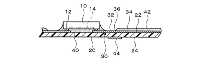
以下、本発明の実施の形態を、図面を参照して説明する。図1は、本発明の実施の形態に係る半導体装置を説明する図である。図2は、図1に示す半導体装置をその基板を屈曲させて示す図である。 Hereinafter, embodiments of the present invention will be described with reference to the drawings. FIG. 1 is a diagram for explaining a semiconductor device according to an embodiment of the present invention. FIG. 2 shows the semiconductor device shown in FIG. 1 with its substrate bent.
半導体装置は、半導体チップ10を有する。半導体チップ10は、電極(図1の例では複数の電極)12を有する。電極12は、パッド及びその上のバンプを含んでもよい。電極12は、半導体チップ10の端部(半導体チップ10が矩形であれば、相互に反対側の2辺に沿った両端部あるいは4辺に沿った周端部)に配列されている。電極12は、半導体チップ10の内部に電気的に接続されている。半導体チップ10(例えば電極12が形成された面)には、集積回路14が作り込まれている。全ての電極12又は全てではないが複数の電極12が、集積回路14に電気的に接続されている。
The semiconductor device has a
半導体装置は、基板(例えばフィルム)20を有する。基板20は、長尺形状のテープであってもよい。基板20は、ポリイミドなどの樹脂で構成されていてもよい。基板20は、撓む性質を有しており、フレキシブル基板ということができる。基板20は、相互に反対方向を向く第1及び第2の面22,24を有する。第1及び第2の面22,24の間隔が、基板20の厚みである。
The semiconductor device has a substrate (for example, a film) 20. The
基板20(詳しくはその第1の面22)には、配線パターン30が形成されている。配線パターン30は、導電材料(例えば銅などの金属)で形成されている。配線パターン30の全体が基板20とオーバーラップしている。配線パターン30の全体が基板20に取り付けられ(あるいは貼り付けられ又は密着し)てもよい。配線パターン30は、接着剤を介して基板20に接着されていてもよいし、基板20に直接付着していてもよい。配線パターン30は、1つの半導体装置で電気的接続に使用されるものである。したがって、1つの基板(例えば長尺形状のテープ)20を使用して、複数の半導体装置の集合体(アッセンブリ)を製造するときには、1つの基板20には、複数の配線パターン30が形成される。配線パターン30は、複数の配線ライン(複数点を電気的に接続する部分)を有しており、複数のランド(他の部品との電気的な接続に使用される部分(配線ラインよりも幅の広い部分))を有していてもよい。配線パターン30(例えばその配線ライン)は、第1及び第2の部分32,34を有する。第1及び第2の部分32,34は連続する部分である。第1及び第2の部分32,34は、直線状に延びていてもよいし、屈曲していてもよい。
A
半導体チップ10は、基板20(詳しくはその第1の面22)に搭載されている。半導体チップ10は、配線パターン30の第1の部分32とオーバーラップしてもよい。半導体チップ10は、配線パターン30の第2の部分34とオーバーラップしないようになっていてもよい。
The
半導体チップ10は、配線パターン30と電気的に接続されている。電気的接続は、配線パターン30の第1の部分32で図られている。半導体チップ10が、電極12が形成された面が基板20と対向するように配置される場合(フェースダウンボンディング)、電極12と配線パターン30(第1の部分32)が対向する。電極12と配線パターン30(第1の部分32)とは、金属接合されてもよいし、両者間に導電粒子が介在してもよい。変形例として、半導体チップ10を、電極12が形成された面が基板20と反対を向くように配置し、電極12と配線パターン30(第1の部分32)にワイヤ等をボンディングしてもよい。
The
半導体チップ10と基板20との間には樹脂部40が形成されている。樹脂部40は、エポキシ等の樹脂で形成されている。樹脂部40は、半導体チップ10と基板20の間のスペースを埋める。樹脂部40は、電極12と配線パターン30との電気的接続部を封止して、電気的接続部に生じた応力を吸収してもよい。樹脂部40は、半導体チップ10の外側に至る。樹脂部40は、配線パターン30の第1の部分32上に至るが、第2の部分34の上方に至らない。樹脂部40は、配線パターン30の第1及び第2の部分32,34の境目36に達しない。樹脂部40の縁(先端又はエッジ)と、境目36との間に間隔があいていてもよい。すなわち、第1の部分32の境目36から連続する部分上に樹脂部40が載らないようになっていてもよい。
A
樹脂部40は、配線パターンの第1及び第2の部分32,34の境目36(後述するように曲がりやすい部分)に達しないので、基板20及び配線パターン30の曲がりによる樹脂部40の破損が抑制又は防止される。
Since the
基板20(詳しくはその第1の面22)には、第1の層42が形成されている。第1の層42は、絶縁層であり、樹脂で形成されていてもよく、ソルダレジスト層であってもよい。第1の層42は、配線パターン30の第2の部分34を覆うが、第1の部分32を覆わない。すなわち、配線パターン30の、第1の層42に覆われた部分が第2の部分34で、第1の層42から露出した部分が第1の部分32である。樹脂部40は、第1の層42に載らないようになっている。
A
基板20(詳しくはその第2の面24)には、第2の層44が形成されている。第2の層44は、絶縁層であり、樹脂で形成されていてもよく、ソルダレジスト層であってもよい。または、第2の層44は、フィルム等の基板であってもよく、接着剤で基板20に貼り付けられていてもよく、基板20に直接付着していてもよい。
A
第2の層44は、配線パターン30の第1及び第2の部分32,34の境目36とオーバーラップしている。配線パターン30の第2の部分34は、第1の層42によって補強されており、第1の部分32は第1の層42によって補強されていないので、配線パターン30を屈曲させると、境目36に応力が集中しやすい。本実施の形態では、第2の層44が境目36とオーバーラップするので、応力の集中しやすい部分が補強され、配線パターン30の破断が抑制又は防止される。
The
第2の層44は、配線パターン30の第2の部分34(又は第1の層42)とオーバーラップしている。したがって、境目36を確実に補強することができる。第2の層44は、樹脂部40とオーバーラップしない。したがって、第2の層44と樹脂部40との間で、配線パターン30(あるいは基板20)の曲がりが許容される。第2の層44は、樹脂部40及び第1の層42よりも柔らかい材料で形成されていてもよい。樹脂部40は、第1及び第2の層42,44よりも硬い材料で形成されていてもよい。
The
本実施の形態に係る半導体装置の製造方法は、基板20の第1の面22に半導体チップ10を搭載することを含む。その詳細は、上述した内容から導き出すことができる。半導体チップ10を搭載するときに、基板20には既に第1の層42が形成されていてもよい。配線パターン30の第1の部分32で、半導体チップ10と配線パターン30を電気的に接続する。フェースダウンボンディングが適用される場合、半導体チップ10の搭載が完了したときに、半導体チップ10と配線パターン30の電気的接続も完了してもよい。
The method for manufacturing a semiconductor device according to the present embodiment includes mounting the
本実施の形態に係る半導体装置の製造方法は、樹脂部40の形成を含む。その詳細は、上述した内容から導き出すことができる。樹脂部40は、半導体チップ10を基板20に搭載した後に、半導体チップ10と基板20の間に樹脂を充填することで形成してもよい。この場合、樹脂はアンダーフィル材である。
The manufacturing method of the semiconductor device according to the present embodiment includes the formation of the
あるいは、半導体チップ10と基板20の間に、接着剤としての樹脂を介在させて、半導体チップ10を基板20に搭載してもよい。半導体チップ10を搭載するときに、半導体チップ10の下から樹脂を押し出すことで樹脂部40を形成することができる。この場合、半導体チップ10の搭載が完了したときに、半導体チップ10と配線パターン30の電気的接続も完了してもよいし、樹脂部40の形成も完了してもよい。接着剤としての樹脂は、絶縁性樹脂であってもよいし、導電粒子を含有していればこれを電気的接続に使用することができる。
Alternatively, the
本実施の形態に係る半導体装置の製造方法は、基板20の第2の面24に第2の層44を設けることを含む。その詳細は、上述した内容から導き出すことができる。第2の層44は、半導体チップ10の基板20への搭載前に設けてもよいし、半導体チップ10と配線パターン30の電気的接続前に設けてもよいし、樹脂部40の形成前に設けてもよい。あるいは、第2の層44は、半導体チップ10の基板20への搭載後に設けてもよいし、半導体チップ10と配線パターン30の電気的接続後に設けてもよいし、樹脂部40の形成後に設けてもよい。
The method for manufacturing a semiconductor device according to the present embodiment includes providing the
本実施の形態に係る半導体装置の製造方法のその他の詳細は、上述した半導体装置の構成から導き出すことができる内容を含む。 Other details of the manufacturing method of the semiconductor device according to the present embodiment include contents that can be derived from the configuration of the semiconductor device described above.
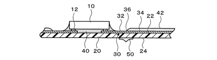
図3は、本発明の実施の形態に係る半導体装置の変形例を説明する図である。図4は、図3に示す半導体装置をその基板を屈曲させて示す図である。図3に示す例では、第2の層50が、配線パターン30の第1及び第2の部分32,34の境目36とオーバーラップする部分が最も厚くなるように形成されている。これによれば、第2の層50の最も厚い部分(すなわち最も補強性能が高い部分)が、配線パターン30の最も応力が集中しやすい部分(すなわち境目36)とオーバーラップするので、配線パターン30の耐性が向上する。その他の構成は、上記実施の形態で説明した内容が該当する。
FIG. 3 is a diagram illustrating a modification of the semiconductor device according to the embodiment of the present invention. FIG. 4 is a diagram showing the semiconductor device shown in FIG. 3 with its substrate bent. In the example shown in FIG. 3, the
図5には、本発明の実施の形態に係る電子モジュール1000が示されている。電子モジュール1000は、上述した半導体装置と、これが取り付けられてなる電子パネル(例えば液晶パネル又はエレクトロルミネセンスパネル等の表示パネル)1100を有する。詳しくは、半導体装置の基板20が電子パネル1100に取り付けられ、配線パターン30が電子パネル1100に電気的に接続される。本発明の実施の形態に係る半導体装置を有する電子機器として、図6にはノート型パーソナルコンピュータ2000が示され、図7には携帯電話3000が示されている。
FIG. 5 shows an
本発明は、上述した実施の形態に限定されるものではなく、種々の変形が可能である。例えば、本発明は、実施の形態で説明した構成と実質的に同一の構成(例えば、機能、方法及び結果が同一の構成、あるいは目的及び結果が同一の構成)を含む。また、本発明は、実施の形態で説明した構成の本質的でない部分を置き換えた構成を含む。また、本発明は、実施の形態で説明した構成と同一の作用効果を奏する構成又は同一の目的を達成することができる構成を含む。また、本発明は、実施の形態で説明した構成に公知技術を付加した構成を含む。さらに、本発明は、実施の形態で説明した技術的事項のいずれかを限定的に除外した内容を含む。あるいは、本発明は、上述した実施の形態から公知技術を限定的に除外した内容を含む。 The present invention is not limited to the above-described embodiments, and various modifications can be made. For example, the present invention includes configurations that are substantially the same as the configurations described in the embodiments (for example, configurations that have the same functions, methods, and results, or configurations that have the same purposes and results). In addition, the invention includes a configuration in which a non-essential part of the configuration described in the embodiment is replaced. In addition, the present invention includes a configuration that exhibits the same operational effects as the configuration described in the embodiment or a configuration that can achieve the same object. Further, the invention includes a configuration in which a known technique is added to the configuration described in the embodiment. Furthermore, the present invention includes contents that exclude any of the technical matters described in the embodiments in a limited manner. Or this invention includes the content which excluded the well-known technique limitedly from embodiment mentioned above.
10…半導体チップ 12…電極 14…集積回路 20…基板 22…第1の面 24…第2の面 30…配線パターン 32…第1の部分 34…第2の部分 36…境目 40…樹脂部 42…第1の層 44…第2の層
DESCRIPTION OF
Claims (12)
連続する第1及び第2の部分を有して前記基板の前記第1の面に形成されてなる配線パターンと、
前記配線パターンの前記第1の部分を除いて前記第2の部分を覆うように形成された第1の層と、
前記基板の前記第1の面に搭載されて、前記第1の部分で前記配線パターンと電気的に接続されてなる半導体チップと、
前記半導体チップと前記基板との間から、前記半導体チップの外側であって前記配線パターンの前記第1の部分上に至るが前記第1及び第2の部分の境目に達しないように設けられた樹脂部と、
前記基板の前記第2の面に、前記配線パターンの前記境目とオーバーラップするとともに、前記樹脂部とオーバーラップしないように設けられてなる第2の層と、
を有する半導体装置。 A substrate having first and second surfaces facing away from each other;
A wiring pattern formed on the first surface of the substrate having a continuous first and second portion;
A first layer formed to cover the second portion except for the first portion of the wiring pattern;
A semiconductor chip mounted on the first surface of the substrate and electrically connected to the wiring pattern at the first portion;
Provided between the semiconductor chip and the substrate, outside the semiconductor chip and on the first portion of the wiring pattern, but not reaching the boundary between the first and second portions. A resin part;
A second layer provided on the second surface of the substrate so as to overlap the boundary of the wiring pattern and not to overlap the resin portion;
A semiconductor device.
前記第2の層は、前記第1の層とオーバーラップする半導体装置。 The semiconductor device according to claim 1,
The second layer is a semiconductor device that overlaps with the first layer.
前記第2の層は、前記境目とオーバーラップする部分が最も厚くなるように形成されてなる半導体装置。 The semiconductor device according to claim 2,
The second layer is a semiconductor device formed so that a portion overlapping the boundary is thickest.
前記第2の層は、樹脂からなる半導体装置。 The semiconductor device according to any one of claims 1 to 3,
The second layer is a semiconductor device made of resin.
前記第1及び第2の層のうち少なくとも一方は、ソルダレジスト層である半導体装置。 The semiconductor device according to any one of claims 1 to 3,
A semiconductor device in which at least one of the first and second layers is a solder resist layer.
前記第2の層は、前記樹脂部及び前記第1の層よりも柔らかい材料で形成されてなる半導体装置。 The semiconductor device according to any one of claims 1 to 5,
The second layer is a semiconductor device formed of a softer material than the resin portion and the first layer.
前記樹脂部は、前記第1及び第2の層よりも硬い材料で形成されてなる半導体装置。 The semiconductor device according to any one of claims 1 to 6,
The resin part is a semiconductor device formed of a material harder than the first and second layers.
前記半導体装置が取り付けられてなる電子パネルと、
を有する電子モジュール。 A semiconductor device according to any one of claims 1 to 7,
An electronic panel to which the semiconductor device is attached;
An electronic module.
前記配線パターンの前記第1の部分で、前記半導体チップと前記配線パターンを電気的に接続すること、
前記半導体チップと前記基板との間から、前記半導体チップの外側であって前記配線パターンの前記第1の部分上に至るが前記第1及び第2の部分の境目に達しないように樹脂部を設けること、及び、
前記基板の前記第1の面とは反対の第2の面に、前記配線パターンの前記境目とオーバーラップするとともに、前記樹脂部とオーバーラップしないように第2の層を設けること、
を含む半導体装置の製造方法。 A first surface of a substrate on which a wiring pattern having continuous first and second portions is formed, the first surface of the wiring pattern excluding the first portion and covering the second portion. Mounting a semiconductor chip on the first surface on which one layer is formed;
Electrically connecting the semiconductor chip and the wiring pattern at the first portion of the wiring pattern;
A resin portion is provided between the semiconductor chip and the substrate so as to reach the first portion of the wiring pattern outside the semiconductor chip but not reaching the boundary between the first and second portions. Providing, and
Providing a second layer on the second surface opposite to the first surface of the substrate so as to overlap the boundary of the wiring pattern and not to overlap the resin portion;
A method of manufacturing a semiconductor device including:
前記第2の層を、前記第1の層とオーバーラップするように設ける半導体装置の製造方法。 The method of manufacturing a semiconductor device according to claim 10.
A method for manufacturing a semiconductor device, wherein the second layer is provided so as to overlap with the first layer.
前記第2の層を、前記境目とオーバーラップする部分が最も厚くなるように形成する半導体装置の製造方法。 The method of manufacturing a semiconductor device according to claim 11.
A method of manufacturing a semiconductor device, wherein the second layer is formed so that a portion overlapping with the boundary is thickest.
Priority Applications (2)
| Application Number | Priority Date | Filing Date | Title |
|---|---|---|---|
| JP2003366080A JP3722223B2 (en) | 2003-10-27 | 2003-10-27 | Semiconductor device and manufacturing method thereof, electronic module, and electronic apparatus |
| US10/973,989 US7176568B2 (en) | 2003-10-27 | 2004-10-26 | Semiconductor device and its manufacturing method, electronic module, and electronic unit |
Applications Claiming Priority (1)
| Application Number | Priority Date | Filing Date | Title |
|---|---|---|---|
| JP2003366080A JP3722223B2 (en) | 2003-10-27 | 2003-10-27 | Semiconductor device and manufacturing method thereof, electronic module, and electronic apparatus |
Publications (2)
| Publication Number | Publication Date |
|---|---|
| JP2005129846A true JP2005129846A (en) | 2005-05-19 |
| JP3722223B2 JP3722223B2 (en) | 2005-11-30 |
Family
ID=34587188
Family Applications (1)
| Application Number | Title | Priority Date | Filing Date |
|---|---|---|---|
| JP2003366080A Expired - Fee Related JP3722223B2 (en) | 2003-10-27 | 2003-10-27 | Semiconductor device and manufacturing method thereof, electronic module, and electronic apparatus |
Country Status (2)
| Country | Link |
|---|---|
| US (1) | US7176568B2 (en) |
| JP (1) | JP3722223B2 (en) |
Cited By (1)
| Publication number | Priority date | Publication date | Assignee | Title |
|---|---|---|---|---|
| JP2012175000A (en) * | 2011-02-23 | 2012-09-10 | Sharp Corp | Semiconductor device and manufacturing method of the same |
Families Citing this family (13)
| Publication number | Priority date | Publication date | Assignee | Title |
|---|---|---|---|---|
| US7176586B2 (en) * | 2003-08-01 | 2007-02-13 | Ledford Timothy Gerard | Grip actuated vehicle control system |
| US7480690B2 (en) * | 2003-12-29 | 2009-01-20 | Xilinx, Inc. | Arithmetic circuit with multiplexed addend inputs |
| US7767543B2 (en) * | 2005-09-06 | 2010-08-03 | Semiconductor Energy Laboratory Co., Ltd. | Method for manufacturing a micro-electro-mechanical device with a folded substrate |
| DE102008028300B4 (en) * | 2008-06-13 | 2021-10-07 | Tdk Electronics Ag | Flexible area printed circuit board and method of manufacture |
| US9797567B2 (en) | 2008-12-11 | 2017-10-24 | Osram Oled Gmbh | Organic-light-emitting diode and luminaire |
| JP5452273B2 (en) * | 2010-02-15 | 2014-03-26 | オリンパス株式会社 | Semiconductor device |
| KR101979361B1 (en) * | 2012-10-25 | 2019-05-17 | 삼성디스플레이 주식회사 | Chip on film and display device including the same |
| KR20140123852A (en) * | 2013-04-15 | 2014-10-23 | 삼성디스플레이 주식회사 | Chip on film and display device having the same |
| KR102176719B1 (en) | 2013-10-14 | 2020-11-10 | 삼성디스플레이 주식회사 | Flexible display panel and manufacturing method thereof |
| US10545917B2 (en) | 2014-02-19 | 2020-01-28 | Snowflake Inc. | Multi-range and runtime pruning |
| US10777498B2 (en) * | 2017-08-29 | 2020-09-15 | Novatek Microelectronics Corp. | Chip on film package with reinforcing sheet |
| KR102481385B1 (en) * | 2017-09-27 | 2022-12-27 | 삼성디스플레이 주식회사 | Foldable display apparatus and the manufacturing method thereof |
| KR20210105723A (en) | 2020-02-19 | 2021-08-27 | 삼성전자주식회사 | Chip-on-film package, and display module and electronic device comprising the same |
Family Cites Families (12)
| Publication number | Priority date | Publication date | Assignee | Title |
|---|---|---|---|---|
| JPS56169568A (en) | 1980-06-03 | 1981-12-26 | Eiichi Shinkawa | Method of making instant hamburger |
| JPS61117266A (en) | 1984-11-14 | 1986-06-04 | Mitsubishi Heavy Ind Ltd | Manufacture of sliding material for parer machine |
| JPH08116140A (en) | 1994-10-18 | 1996-05-07 | Sumitomo Electric Ind Ltd | Flexible printed wiring board |
| US6208521B1 (en) * | 1997-05-19 | 2001-03-27 | Nitto Denko Corporation | Film carrier and laminate type mounting structure using same |
| JP3714779B2 (en) | 1997-11-04 | 2005-11-09 | ティアック株式会社 | Disk drive device |
| DE19923467B4 (en) * | 1999-05-21 | 2004-11-11 | Infineon Technologies Ag | Semiconductor module with several semiconductor chips and conductive connection by means of flexible strips between the semiconductor chips |
| US6683377B1 (en) * | 2000-05-30 | 2004-01-27 | Amkor Technology, Inc. | Multi-stacked memory package |
| JP3565142B2 (en) | 2000-07-03 | 2004-09-15 | セイコーエプソン株式会社 | Wiring board and method of manufacturing the same, semiconductor device, circuit board, and electronic equipment |
| JP2002289984A (en) | 2001-03-26 | 2002-10-04 | Olympus Optical Co Ltd | Double-sided flexible board and camera having the same |
| JP2003051648A (en) | 2001-08-06 | 2003-02-21 | Olympus Optical Co Ltd | Flexible printed board |
| JP4667740B2 (en) | 2002-12-09 | 2011-04-13 | 株式会社フジクラ | Printed wiring board |
| US6841855B2 (en) * | 2003-04-28 | 2005-01-11 | Intel Corporation | Electronic package having a flexible substrate with ends connected to one another |
-
2003
- 2003-10-27 JP JP2003366080A patent/JP3722223B2/en not_active Expired - Fee Related
-
2004
- 2004-10-26 US US10/973,989 patent/US7176568B2/en not_active Expired - Fee Related
Cited By (2)
| Publication number | Priority date | Publication date | Assignee | Title |
|---|---|---|---|---|
| JP2012175000A (en) * | 2011-02-23 | 2012-09-10 | Sharp Corp | Semiconductor device and manufacturing method of the same |
| US8598692B2 (en) | 2011-02-23 | 2013-12-03 | Sharp Kabushiki Kaisha | Semiconductor device and method for manufacturing same |
Also Published As
| Publication number | Publication date |
|---|---|
| US7176568B2 (en) | 2007-02-13 |
| US20050110049A1 (en) | 2005-05-26 |
| JP3722223B2 (en) | 2005-11-30 |
Similar Documents
| Publication | Publication Date | Title |
|---|---|---|
| KR100652519B1 (en) | Tape substrate comprising dual metal layer and chip on film package using the same | |
| JP4024773B2 (en) | WIRING BOARD, SEMICONDUCTOR DEVICE, ITS MANUFACTURING METHOD, AND SEMICONDUCTOR MODULE DEVICE | |
| JP3722223B2 (en) | Semiconductor device and manufacturing method thereof, electronic module, and electronic apparatus | |
| JP2006060128A (en) | Semiconductor device | |
| US20110204497A1 (en) | Semiconductor integrated circuit and method for manufacturing the same | |
| JP4740708B2 (en) | Wiring board and semiconductor device | |
| JP2005079581A (en) | Tape substrate, semiconductor chip package using tape substrate, and lcd device using semiconductor chip package | |
| JP5567362B2 (en) | Display device and electronic device | |
| KR100658442B1 (en) | Tape package of heat spreading type and flat panel display using the same | |
| JP3687610B2 (en) | Semiconductor device, circuit board, and electronic equipment | |
| KR20210025167A (en) | Display device | |
| US6853080B2 (en) | Electronic device and method of manufacturing the same, and electronic instrument | |
| JP2004128356A (en) | Semiconductor device | |
| JP3867796B2 (en) | Semiconductor device and manufacturing method thereof, circuit board, and electronic apparatus | |
| CN111445801A (en) | Display panel and display device | |
| JP4513969B2 (en) | Electronic devices | |
| JP4310631B2 (en) | Semiconductor device, circuit board and electronic equipment | |
| JP4013070B2 (en) | Integrated circuit chip, electronic device, manufacturing method thereof, and electronic apparatus | |
| WO2011055548A1 (en) | Substrate connection structure | |
| JP3685196B2 (en) | WIRING BOARD, SEMICONDUCTOR DEVICE, ITS MANUFACTURING METHOD, AND ELECTRONIC DEVICE | |
| TWI515492B (en) | Package structure and display module | |
| JP2006332415A (en) | Semiconductor device | |
| JP2008140925A (en) | Semiconductor device and its manufacturing method, and display device | |
| JP2007149863A (en) | Method of manufacturing electronic apparatus | |
| JP2011253880A (en) | Electronic component mounting board and method of manufacturing the same |
Legal Events
| Date | Code | Title | Description |
|---|---|---|---|
| A871 | Explanation of circumstances concerning accelerated examination |
Free format text: JAPANESE INTERMEDIATE CODE: A871 Effective date: 20050208 |
|
| A975 | Report on accelerated examination |
Free format text: JAPANESE INTERMEDIATE CODE: A971005 Effective date: 20050304 |
|
| A131 | Notification of reasons for refusal |
Free format text: JAPANESE INTERMEDIATE CODE: A131 Effective date: 20050308 |
|
| A521 | Written amendment |
Free format text: JAPANESE INTERMEDIATE CODE: A523 Effective date: 20050411 |
|
| A131 | Notification of reasons for refusal |
Free format text: JAPANESE INTERMEDIATE CODE: A131 Effective date: 20050510 |
|
| A521 | Written amendment |
Free format text: JAPANESE INTERMEDIATE CODE: A523 Effective date: 20050704 |
|
| TRDD | Decision of grant or rejection written | ||
| A01 | Written decision to grant a patent or to grant a registration (utility model) |
Free format text: JAPANESE INTERMEDIATE CODE: A01 Effective date: 20050824 |
|
| A61 | First payment of annual fees (during grant procedure) |
Free format text: JAPANESE INTERMEDIATE CODE: A61 Effective date: 20050906 |
|
| R150 | Certificate of patent or registration of utility model |
Free format text: JAPANESE INTERMEDIATE CODE: R150 |
|
| FPAY | Renewal fee payment (event date is renewal date of database) |
Free format text: PAYMENT UNTIL: 20080922 Year of fee payment: 3 |
|
| FPAY | Renewal fee payment (event date is renewal date of database) |
Free format text: PAYMENT UNTIL: 20090922 Year of fee payment: 4 |
|
| FPAY | Renewal fee payment (event date is renewal date of database) |
Free format text: PAYMENT UNTIL: 20090922 Year of fee payment: 4 |
|
| FPAY | Renewal fee payment (event date is renewal date of database) |
Free format text: PAYMENT UNTIL: 20100922 Year of fee payment: 5 |
|
| FPAY | Renewal fee payment (event date is renewal date of database) |
Free format text: PAYMENT UNTIL: 20100922 Year of fee payment: 5 |
|
| FPAY | Renewal fee payment (event date is renewal date of database) |
Free format text: PAYMENT UNTIL: 20110922 Year of fee payment: 6 |
|
| FPAY | Renewal fee payment (event date is renewal date of database) |
Free format text: PAYMENT UNTIL: 20120922 Year of fee payment: 7 |
|
| FPAY | Renewal fee payment (event date is renewal date of database) |
Free format text: PAYMENT UNTIL: 20130922 Year of fee payment: 8 |
|
| LAPS | Cancellation because of no payment of annual fees |