JP2005105281A - Silicious film-forming composition, silicious film and its forming method, and electronic part having silicious film - Google Patents
Silicious film-forming composition, silicious film and its forming method, and electronic part having silicious film Download PDFInfo
- Publication number
- JP2005105281A JP2005105281A JP2004302043A JP2004302043A JP2005105281A JP 2005105281 A JP2005105281 A JP 2005105281A JP 2004302043 A JP2004302043 A JP 2004302043A JP 2004302043 A JP2004302043 A JP 2004302043A JP 2005105281 A JP2005105281 A JP 2005105281A
- Authority
- JP
- Japan
- Prior art keywords
- silica
- forming
- atom
- composition
- film
- Prior art date
- Legal status (The legal status is an assumption and is not a legal conclusion. Google has not performed a legal analysis and makes no representation as to the accuracy of the status listed.)
- Withdrawn
Links
Images
Abstract
Description
本発明は、シリカ系被膜形成用組成物、シリカ系被膜及びその形成方法、並びにシリカ系被膜を備える電子部品に関する。 The present invention relates to a composition for forming a silica-based film, a silica-based film and a method for forming the same, and an electronic component including the silica-based film.
従来、CVD法によって形成され、4.2程度の比誘電率を有するSiO2膜が層間絶縁膜の形成材料として用いられてきた。しかし、デバイスの配線間容量を低減し、LSIの動作速度を向上させる観点から、更なる低誘電率を発現できる材料が切望されていた。 Conventionally, a SiO 2 film formed by a CVD method and having a relative dielectric constant of about 4.2 has been used as a material for forming an interlayer insulating film. However, from the viewpoint of reducing the inter-wiring capacitance of the device and improving the operation speed of the LSI, a material capable of developing a further low dielectric constant has been desired.
この要望に対し、3.5程度の比誘電率を有し、CVD法で形成されるSiOF膜が開発された。さらに、2.5〜3.0の比誘電率を有する絶縁材料として、有機SOG(Spin On Glass)、有機ポリマー等が開発された。さらにまた、比誘電率が2.5以下の絶縁材料として、被膜中に空隙を有するポーラス材料が有効と考えられており、LSIの層間絶縁膜に適用するための検討・開発が盛んに行われている。 In response to this demand, a SiOF film having a relative dielectric constant of about 3.5 and formed by a CVD method has been developed. Furthermore, organic SOG (Spin On Glass), an organic polymer, etc. were developed as an insulating material which has a dielectric constant of 2.5-3.0. Furthermore, a porous material having voids in the coating is considered to be effective as an insulating material having a relative dielectric constant of 2.5 or less, and studies and developments for application to an interlayer insulating film of LSI are actively conducted. ing.
このようなポーラス材料の形成方法として、下記特許文献1及び2には有機SOGを用いる方法が提案されている。この方法においては、金属アルコキシドの加水分解縮重合物と揮発又は分解特性を有するポリマーとを含む組成物を加熱して被膜を形成した後、この被膜を加熱して該被膜中に空孔を形成させてポーラス材料を得る。
ところで、LSI等の半導体素子といった電子デバイス部品においては、高集積化による配線の微細化に伴い、配線間容量の増大による信号遅延時間の増大が問題となっている。このため、電子デバイス部品の絶縁材料に対して、耐熱性、機械特性等の他、更なる低比誘電率と熱処理工程の短縮が求められている。 By the way, in electronic device parts such as semiconductor elements such as LSIs, an increase in signal delay time due to an increase in inter-wiring capacitance has become a problem with the miniaturization of wiring due to high integration. For this reason, in addition to heat resistance, mechanical characteristics, and the like, there is a demand for further reduction of the dielectric constant and heat treatment process for the insulating material of electronic device components.
一般に、配線の信号伝搬速度(v)と、配線材料が接する絶縁材料の比誘電率(ε)との間には、式;v=k/√εで表される関係を有する(式中のkは定数である)。つまり、使用する周波数領域を高くすると共に、絶縁材料の比誘電率(ε)を低減することにより、信号伝搬の高速化が達成される。 In general, there is a relationship represented by the equation: v = k / √ε between the signal propagation speed (v) of the wiring and the relative dielectric constant (ε) of the insulating material in contact with the wiring material (where k is a constant). That is, by increasing the frequency region to be used and reducing the relative dielectric constant (ε) of the insulating material, signal transmission speed can be increased.
ここで、本発明者は上述の従来の方法について詳細に検討を行ったところ、絶縁膜に要求される所望の低誘電率を達成するためには、極めて多量の空孔(空隙)を絶縁膜中に導入する必要があることを見出した。さらに、本発明者は、膜のベース材料となる有機SOGの機械的な膜強度又は膜硬度が本来的に不足している場合に空隙率が過度に高まると、膜の機械強度が一層低下してしまう傾向があることを見出した。しかしながら、絶縁膜の比誘電率が低下するにつれて膜強度が低下する傾向にあるため、従来のプロセスを適合させることは大きな問題がある。 Here, the inventor has examined the above-described conventional method in detail, and in order to achieve a desired low dielectric constant required for the insulating film, an extremely large number of holes (voids) are formed in the insulating film. Found that it needs to be introduced in. Furthermore, the present inventors have found that when the mechanical film strength or film hardness of organic SOG as a film base material is inherently insufficient, the mechanical strength of the film is further reduced when the porosity is excessively increased. I found out that there is a tendency to end up. However, since the film strength tends to decrease as the dielectric constant of the insulating film decreases, it is a big problem to adapt the conventional process.
また、被膜形成用組成物を硬化させて被膜を形成させるためには、450℃以上の高温雰囲気が必要である。しかも、最終的に硬化が終了するまでには、1時間程度の長時間を要する傾向にある。このため、かかる被膜を層間絶縁膜として用いた場合、この被膜形成プロセスにおける入熱量(サーマルバジェット)によって他の層、特に配線層の劣化が懸念される。また、入熱量の増加に伴って基板の反りが顕著となるといった問題も生じ得る。 Further, in order to cure the film forming composition and form a film, a high temperature atmosphere of 450 ° C. or higher is required. Moreover, it tends to take a long time of about one hour until the curing is finally completed. For this reason, when such a film is used as an interlayer insulating film, there is a concern about deterioration of other layers, particularly the wiring layer, due to the heat input (thermal budget) in the film forming process. Moreover, the problem that the curvature of a board | substrate becomes remarkable with the increase in the amount of heat inputs may also arise.
さらに、上述の如く、高集積化による配線の微細化が加速しており、半導体デバイスを構成する各部材層の薄層化・多層化、及び配線層等の材料変更が進んでいる。入熱量による各層の材料劣化の影響は今まで以上に増大すると予想されるため、各プロセスでの熱負荷の低減による熱履歴の改善が急務となっている。 Further, as described above, miniaturization of wiring due to high integration is accelerating, and thinning and multilayering of each member layer constituting a semiconductor device and change of materials such as wiring layers are progressing. Since the influence of material deterioration of each layer due to the amount of heat input is expected to increase more than ever, there is an urgent need to improve the thermal history by reducing the thermal load in each process.
そこで、本発明はかかる事情に鑑みてなされたものであり、低誘電性に優れると共に、充分な機械的強度を有し、従来に比して低温、短時間で硬化可能なシリカ系被膜を形成できるシリカ系被膜形成用組成物、かかる組成物からなるシリカ系被膜及びその形成方法、並びにかかるシリカ系被膜を備える電子部品を提供することを目的とする。 Therefore, the present invention has been made in view of such circumstances, and forms a silica-based coating that is excellent in low dielectric properties, has sufficient mechanical strength, and can be cured at a low temperature and in a short time compared to the prior art. An object of the present invention is to provide a composition for forming a silica-based film, a silica-based film comprising the composition, a method for forming the composition, and an electronic component including the silica-based film.
上記目的を達成するために、本発明者らは、絶縁膜に好適なシリカ系被膜を得るための材料成分及びその組成の観点から鋭意研究を重ねた結果、特定の成分を含有する組成物が、従来の種々の問題点を解消し得ることを見出し、本発明を完成するに至った。 In order to achieve the above object, the present inventors have conducted extensive research from the viewpoints of material components and composition thereof for obtaining a silica-based film suitable for an insulating film, and as a result, a composition containing a specific component is obtained. The present inventors have found that various conventional problems can be solved and have completed the present invention.
すなわち、本発明は、(a)成分:下記一般式(1);
R1 nSiX4−n …(1)
[式中、R1はH原子若しくはF原子、又はB原子、N原子、Al原子、P原子、Si原子、Ge原子若しくはTi原子を含む基、又は炭素数1〜20の有機基を示し、Xは加水分解性基を示し、nは0〜2の整数を示す。但し、nが2のとき、各R1は同一でも異なっていてもよく、nが0〜2のとき、各Xは同一でも異なっていてもよい。]、
で表される化合物を加水分解縮合して得られるシロキサン樹脂と、(b)成分:少なくとも1種の非プロトン性溶媒を含む有機溶媒と、(c)成分:オニウム塩と、(d)成分:250〜500℃の加熱温度において熱分解又は揮発する空隙形成用化合物と、を含有してなるシリカ系被膜形成用組成物を提供する。
That is, the present invention comprises (a) component: the following general formula (1);
R 1 n SiX 4-n (1)
[Wherein R 1 represents an H atom or an F atom, or a group containing a B atom, an N atom, an Al atom, a P atom, a Si atom, a Ge atom or a Ti atom, or an organic group having 1 to 20 carbon atoms, X represents a hydrolyzable group, and n represents an integer of 0 to 2. However, when n is 2, each R 1 may be the same or different, and when n is 0 to 2, each X may be the same or different. ],
A siloxane resin obtained by hydrolytic condensation of a compound represented by the formula: (b) component: an organic solvent containing at least one aprotic solvent, (c) component: an onium salt, and (d) component: A composition for forming a silica-based film comprising a void-forming compound that thermally decomposes or volatilizes at a heating temperature of 250 to 500 ° C.
本発明のシリカ系被膜形成用組成物は、被膜形成成分として上記構成のシロキサン樹脂を含み、シロキサン樹脂を溶解させる有機溶媒成分として非プロトン性溶媒を必須成分とし、オニウム塩を更に含有することから、低誘電性、特に高周波領域(100kHz以上の高周波領域で、例えば1MHz)における低誘電性に優れると共に、充分な機械的強度を有し、従来に比して低温且つ短時間で硬化可能なシリカ系被膜を形成できるようになる。また、上記組成物の低温且つ短時間での硬化が可能となることから、被膜形成プロセスにおける入熱量も軽減される。したがって、配線層等の劣化や基板の反り等の問題も解消できる。さらに、被膜の膜厚の均一性も向上させることができる。 The composition for forming a silica-based film of the present invention contains the siloxane resin having the above-described structure as a film-forming component, an aprotic solvent as an essential component as an organic solvent component for dissolving the siloxane resin, and further containing an onium salt. Silica that is excellent in low dielectric property, especially in high frequency region (high frequency region of 100 kHz or higher, for example, 1 MHz), has sufficient mechanical strength, and can be cured at a lower temperature and in a shorter time than conventional. A system film can be formed. Further, since the composition can be cured at a low temperature in a short time, the amount of heat input in the film forming process is also reduced. Therefore, problems such as deterioration of the wiring layer and the warp of the substrate can be solved. Furthermore, the uniformity of the film thickness can also be improved.
上記効果が生じる要因は必ずしも明らかではないが、シリカ系被膜が低誘電性及び充分な機械的強度を有するようになるのは、上記シロキサン樹脂と非プロトン性溶媒を使用したことに主に起因しており、低温且つ短時間での硬化が可能となるのは、非プロトン性溶媒とオニウム塩を使用したことに主に起因しているものと推測される。また、被膜の膜厚の均一性の向上は、非プロトン性溶媒を使用したことに主に起因していると考えられる。 The cause of the above effect is not necessarily clear, but the silica-based coating has low dielectric constant and sufficient mechanical strength mainly due to the use of the siloxane resin and aprotic solvent. The reason why the curing at a low temperature and in a short time is possible is mainly due to the use of an aprotic solvent and an onium salt. Moreover, it is thought that the improvement in the uniformity of the film thickness is mainly due to the use of an aprotic solvent.
また、本発明のシリカ系被膜形成用組成物は250〜500℃の加熱温度において熱分解又は揮発する空隙形成用化合物を更に含有してなる。かかる構成のシリカ系被膜形成用組成物は、機械的強度の著しい低下を抑制しつつ、低誘電率化を達成可能なシリカ系被膜を形成できる。 The composition for forming a silica-based film of the present invention further contains a void-forming compound that is thermally decomposed or volatilized at a heating temperature of 250 to 500 ° C. The composition for forming a silica-based film having such a configuration can form a silica-based film capable of achieving a low dielectric constant while suppressing a significant decrease in mechanical strength.
また、非プロトン性溶媒が、エーテル系溶媒及びケトン系溶媒からなる群より選ばれる少なくとも1種の非プロトン性溶媒を含むことが好ましく、2価アルコールのジアルキルエ−テル、2価アルコールのアルキルエステルエーテル、2価アルコールのジエステル及び環状ケトンからなる群より選ばれる少なくとも1種の非プロトン性溶媒を含むことが好ましく、上記非プロトン性溶媒の少なくとも1種は、10以上の非誘電率を有する非プロトン性溶媒であることが好ましい。さらにまた、上記10以上の比誘電率を有する非プロトン性溶媒の含有量が、(b)成分の重量基準で50質量%以上であることがより一層好ましい。 The aprotic solvent preferably contains at least one aprotic solvent selected from the group consisting of ether solvents and ketone solvents, and dialkyl ethers of dihydric alcohols and alkyl ester ethers of dihydric alcohols. It is preferable to include at least one aprotic solvent selected from the group consisting of diesters of dihydric alcohols and cyclic ketones, and at least one of the aprotic solvents is an aprotic having a non-dielectric constant of 10 or more. It is preferable that it is an organic solvent. Furthermore, the content of the aprotic solvent having a relative dielectric constant of 10 or more is more preferably 50% by mass or more based on the weight of the component (b).
また、上記非プロトン性溶媒の含有量は、(b)成分の重量基準で80質量%以上であることが好ましい。(b)成分に占める非プロトン性溶媒の含有割合が少ないと、上記組成物の硬化時における低温度化と短時間化を妨げる恐れがある。また、被膜の比誘電率の上昇や機械強度の低下を招く恐れがある。 The content of the aprotic solvent is preferably 80% by mass or more based on the weight of the component (b). When the content ratio of the aprotic solvent in the component (b) is small, there is a possibility that the temperature reduction and the time shortening at the time of curing of the composition may be hindered. Further, there is a risk of increasing the relative dielectric constant of the film and decreasing the mechanical strength.
特に、10以上の非誘電率を有する非プロトン性溶媒を有機溶媒成分として備えるシリカ系被膜形成用組成物は、後述の空隙形成用化合物を含有して空隙(空孔)を形成した際に空隙の分布が狭くなる傾向にある。 In particular, a composition for forming a silica-based film comprising an aprotic solvent having a non-dielectric constant of 10 or more as an organic solvent component contains a compound for forming voids described later and forms voids (holes). Tend to be narrower.
また、上記(a)成分は、Si原子1モルに対する、H原子、F原子、B原子、N原子、Al原子、P原子、Si原子、Ge原子、Ti原子及びC原子から成る群より選ばれる少なくとも一種の原子の総含有割合が0.65モル以下のものであることが好ましい。 The component (a) is selected from the group consisting of H atom, F atom, B atom, N atom, Al atom, P atom, Si atom, Ge atom, Ti atom and C atom with respect to 1 mol of Si atom. It is preferable that the total content of at least one atom is 0.65 mol or less.
上記構成を有するシリカ系被膜形成用組成物は、シリカ系被膜の他の膜(層)との接着性及び機械的強度の低下が抑制される。したがって、シリカ系被膜上に被着されたCu等の金属配線層をCMP(Chemical Mechanical Polish)する工程において、界面剥離が生じることをも防止できる。 In the composition for forming a silica-based film having the above-described configuration, a decrease in adhesiveness with other films (layers) of the silica-based film and mechanical strength is suppressed. Therefore, it is possible to prevent the occurrence of interfacial delamination in a CMP (Chemical Mechanical Polish) process for a metal wiring layer such as Cu deposited on the silica-based film.
また、上記オニウム塩はアンモニウム塩であることが好ましい。かかる構成を有するシリカ系被膜形成用組成物は、該組成物の安定性を高めることができ、シリカ系被膜の電気特性及び機械特性もより向上させることが可能となる。 The onium salt is preferably an ammonium salt. The composition for forming a silica-based film having such a configuration can improve the stability of the composition, and can further improve the electrical characteristics and mechanical properties of the silica-based film.
更に上記アンモニウム塩の中でもシリカ系被膜の電気特性をより向上させる観点からテトラメチルアンモニウム硝酸塩、テトラメチルアンモニウム酢酸塩、テトラメチルアンモニウムプロピオン酸塩、テトラメチルアンモニウムマレイン酸塩及びテトラメチルアンモニウム硫酸塩からなる群より選ばれる1種以上のアンモニウム塩を用いることがより好ましい。 Further, among the above ammonium salts, tetramethylammonium nitrate, tetramethylammonium acetate, tetramethylammonium propionate, tetramethylammonium maleate and tetramethylammonium sulfate are used from the viewpoint of further improving the electrical properties of the silica-based coating. It is more preferable to use one or more ammonium salts selected from the group.
上記空隙形成用化合物が、ビニルエーテル系化合物、ポリオキシエチレン単位を有するビニル系化合物、ポリオキシプロピレン単位を有するビニル系化合物、ビニルピリジン系化合物、スチレン系化合物、アルキルエステルビニル系化合物、(メタ)アクリレート酸系化合物、ポリオキシアルキレン単位を有する重合体、及びポリカーボネート重合体からなる群より選ばれる1種以上の化合物であることが好ましい。また、上記空隙形成用化合物が、ポリオキシアルキレン単位を有する重合体であることがより好ましい。さらに、上記空隙形成用化合物が、ポリオキシプロピレン単位を有する重合体であることが特に好ましい。 The void-forming compound is a vinyl ether compound, a vinyl compound having a polyoxyethylene unit, a vinyl compound having a polyoxypropylene unit, a vinyl pyridine compound, a styrene compound, an alkyl ester vinyl compound, (meth) acrylate One or more compounds selected from the group consisting of an acid compound, a polymer having a polyoxyalkylene unit, and a polycarbonate polymer are preferred. The void-forming compound is more preferably a polymer having a polyoxyalkylene unit. Furthermore, the void forming compound is particularly preferably a polymer having a polyoxypropylene unit.
空隙形成用化合物が上記化合物である場合のシリカ系被膜形成用組成物は、機械的強度の著しい低下をより抑制し、低誘電率化をより達成可能なシリカ系被膜を形成できる。 The composition for forming a silica-based film in the case where the void-forming compound is the above compound can form a silica-based film that can further suppress a significant decrease in mechanical strength and can achieve a lower dielectric constant.
また、上記空隙形成用化合物は、シリカ系被膜中に微細孔を徐々に形成するものであることが好ましい。シリカ系被膜中に微細孔(空隙、空孔)を徐々に形成することで、最終硬化時に空孔の更なる微細化及び形状の均一化を図ることができる。 Moreover, it is preferable that the said space | gap formation compound is what forms a micropore gradually in a silica-type film. By gradually forming micropores (voids, vacancies) in the silica-based coating, it is possible to further refine the pores and make the shape uniform during final curing.
本発明はまた、基板上にシリカ系被膜を形成する方法であって、上記本発明のシリカ系被膜形成用組成物を基板上に塗布して塗布膜を形成し、該塗布膜に含まれる有機溶媒を除去した後、該塗布膜を250〜500℃の加熱温度で焼成することを特徴とするシリカ系被膜の形成方法を提供する。 The present invention is also a method for forming a silica-based film on a substrate, wherein the composition for forming a silica-based film of the present invention is applied onto a substrate to form a coating film, and an organic contained in the coating film Provided is a method for forming a silica-based film, wherein after removing the solvent, the coating film is baked at a heating temperature of 250 to 500 ° C.
本発明は更に、基板上に設けられており、上記シリカ系被膜の形成方法により形成されてなることを特徴とするシリカ系被膜を提供し、かかる被膜は、特に、基板上に設けられた複数の導電性層のうち互いに隣設された導電性層の間に形成されたもの、すなわち、リーク電流を充分に低減する必要のある絶縁膜、例えば層間絶縁膜として有用である。 The present invention further provides a silica-based coating provided on a substrate and formed by the above-described method for forming a silica-based coating, and in particular, the coating includes a plurality of such coatings provided on the substrate. Of these conductive layers, the conductive layer is useful as an insulating film formed between adjacent conductive layers, that is, an insulating film that needs to sufficiently reduce leakage current, for example, an interlayer insulating film.
そして、本発明は、基板上に本発明によるシリカ系被膜が形成されてなる電子部品を提供する。かかる電子部品は、半導体装置といった電子デバイスを構成するものである。 And this invention provides the electronic component by which the silica type coating film by this invention is formed on a board | substrate. Such an electronic component constitutes an electronic device such as a semiconductor device.
以上説明したように、本発明によれば、2.5以下の低誘電率を100kHz以上の高周波領域においても発揮できると共に、充分な機械的強度を有し、従来に比して低温、短時間で硬化可能なシリカ系被膜を形成できるシリカ系被膜形成用組成物が提供される。また、かかる組成物からなるシリカ系被膜及びその形成方法、並びにかかるシリカ系被膜を備える電子部品が提供される。 As described above, according to the present invention, a low dielectric constant of 2.5 or less can be exhibited even in a high-frequency region of 100 kHz or more, it has sufficient mechanical strength, and has a lower temperature and a shorter time than conventional. There is provided a composition for forming a silica-based film capable of forming a silica-based film that can be cured at a low temperature. Moreover, the silica-type film which consists of this composition, its formation method, and an electronic component provided with this silica-type film are provided.
以下、本発明の実施形態について詳細に説明する。本発明にかかるシリカ系被膜形成用組成物は、(a)〜(c)成分を含有しているが、本発明において特徴的なことは、(b)成分として少なくとも1種の非プロトン性溶媒、すなわち比誘電率の高い極性溶媒を含むシリカ系被膜形成用組成物とすることである。以下、本発明のシリカ系被膜形成用組成物の各成分について詳細に説明する。 Hereinafter, embodiments of the present invention will be described in detail. The composition for forming a silica-based film according to the present invention contains the components (a) to (c). What is characteristic in the present invention is that at least one aprotic solvent is used as the component (b). That is, it is to make the composition for forming a silica-based film containing a polar solvent having a high relative dielectric constant. Hereinafter, each component of the composition for forming a silica-based film of the present invention will be described in detail.
〈(a)成分〉
本発明において、(a)成分として用いられるシロキサン樹脂は、後述のシリカ系被膜の被膜形成成分として機能する。かかる機能を発揮するために、本発明のシリカ系被膜形成用組成物は、(a)成分として下記式(1)で表される化合物を加水分解縮合して得られるシロキサン樹脂を含有する。
R1 nSiX4−n …(1)
上記一般式(1)中、R1は、H原子若しくはF原子、又はB原子、N原子、Al原子、P原子、Si原子、Ge原子若しくはTi原子を含む基、又は炭素数1〜20の有機基(好ましくは炭素数1〜12、更に好ましくは1〜6の有機基)を示す。
<(A) component>
In the present invention, the siloxane resin used as the component (a) functions as a film forming component of the silica-based film described later. In order to exhibit such a function, the composition for forming a silica-based film of the present invention contains a siloxane resin obtained by hydrolytic condensation of a compound represented by the following formula (1) as the component (a).
R 1 n SiX 4-n (1)
In the general formula (1), R 1 is an H atom or F atom, or a group containing a B atom, an N atom, an Al atom, a P atom, a Si atom, a Ge atom, or a Ti atom, or a carbon number of 1 to 20 An organic group (preferably an organic group having 1 to 12 carbon atoms, more preferably 1 to 6 carbon atoms) is shown.
また、シロキサン樹脂のシロキサン結合を形成しているSi原子の1原子あたりに結合しているH原子、F原子、B原子、N原子、Al原子、P原子、Si原子、Ge原子、Ti原子及びC原子から成る群より選ばれる少なくとも一種の原子(以下、「特定の結合原子」という)の総数(M)が0.65以下であることが好ましく、0.55以下であるとより好ましく、0.50以下であると特に好ましく、0.45以下であると極めて好ましい。また、Mの下限値としては0.20程度が好ましい。 In addition, H atom, F atom, B atom, N atom, Al atom, P atom, Si atom, Ge atom, Ti atom bonded to one atom of the Si atom forming the siloxane bond of the siloxane resin, and The total number (M) of at least one atom selected from the group consisting of C atoms (hereinafter referred to as “specific bonding atom”) is preferably 0.65 or less, more preferably 0.55 or less, and 0 .50 or less is particularly preferable, and 0.45 or less is extremely preferable. Further, the lower limit of M is preferably about 0.20.
Mの値が、0.65を超える場合には、最終的に得られるシリカ系被膜の他の膜(層)との接着性、機械強度等が劣る傾向がある。一方、Mの値が0.20未満であると、絶縁膜として用いたときの誘電特性が劣る傾向にある。なお、シロキサン樹脂は、上記特定の結合原子の中でも、シリカ系被膜の成膜性の点で、H原子、F原子、N原子、Si原子、Ti原子及びC原子のうちの少なくとも一種を含むとより好ましく、それらのなかでも誘電特性及び機械強度の点において、H原子、F原子、N原子、Si原子及びC原子のうち少なくとも一種を含むと一層好ましい。 When the value of M exceeds 0.65, the adhesion of the finally obtained silica-based film to other films (layers), mechanical strength, etc. tend to be inferior. On the other hand, if the value of M is less than 0.20, the dielectric characteristics when used as an insulating film tend to be inferior. The siloxane resin contains at least one of H atom, F atom, N atom, Si atom, Ti atom, and C atom in terms of the film-forming property of the silica-based coating among the above specific bonding atoms. Among these, it is more preferable that at least one of H atom, F atom, N atom, Si atom and C atom is contained in terms of dielectric properties and mechanical strength.
なお、Mの値は、シロキサン樹脂の原料である上記一般式(1)で表される化合物の仕込み量から求めることができる。例えば、下記式;
M=[M1+(M2/2)+(M3/3)]/MSi
を用いて算出することができる。式中、M1は特定の結合原子のうち単一の(ただ1つの)Si原子と結合している原子の総数を示し、M2は特定の結合原子のうち2つのケイ素原子で共有されている原子の総数を示し、M3は特定の結合原子のうち3つのケイ素原子で共有されている原子の総数を示し、MSiはSi原子の総数を示す。
In addition, the value of M can be calculated | required from the preparation amount of the compound represented by the said General formula (1) which is a raw material of siloxane resin. For example:
M = [M 1 + (M 2/2) + (
Can be used to calculate. In the formula, M 1 represents the total number of atoms bonded to a single (only one) Si atom among specific bonding atoms, and M 2 is shared by two silicon atoms among the specific bonding atoms. M 3 represents the total number of atoms shared by three silicon atoms among the specific bonded atoms, and M Si represents the total number of Si atoms.
上記一般式(1)に戻り、Xは加水分解性基を示す。Xとしては、例えば、アルコキシ基、ハロゲン原子、アセトキシ基、イソシアネート基、ヒドロキシル基が挙げられ、アルコキシ基であることが好ましい。Xをアルコキシ基とすることにより、上記組成物の液状安定性や塗布特性等が優れるようになる。 Returning to the general formula (1), X represents a hydrolyzable group. Examples of X include an alkoxy group, a halogen atom, an acetoxy group, an isocyanate group, and a hydroxyl group, and an alkoxy group is preferable. By making X an alkoxy group, the liquid stability and coating characteristics of the composition are improved.
加水分解性基Xがアルコキシ基である場合の上記一般式(1)で表される化合物としては、テトラアルコキシシラン、トリアルコキシシラン、ジオルガノジアルコキシシラン等が挙げられる。テトラアルコキシシランとしては、テトラメトキシシラン、テトラエトキシシラン、テトラ−n−プロポキシシラン、テトラ−iso−プロポキシシラン、テトラ−n−ブトキシシラン、テトラ−sec−ブトキシシラン、テトラ−tert−ブトキシシラン、テトラフェノキシシラン等が例示できる。 Examples of the compound represented by the general formula (1) when the hydrolyzable group X is an alkoxy group include tetraalkoxysilane, trialkoxysilane, and diorganodialkoxysilane. Tetraalkoxysilanes include tetramethoxysilane, tetraethoxysilane, tetra-n-propoxysilane, tetra-iso-propoxysilane, tetra-n-butoxysilane, tetra-sec-butoxysilane, tetra-tert-butoxysilane, tetra Examples thereof include phenoxysilane.
トリアルコキシシランとしては、トリメトキシシラン、トリエトキシシラン、トリプロポキシシラン、フルオロトリメトキシシラン、フルオロトリエトキシシラン、メチルトリメトキシシラン、メチルトリエトキシシラン、メチルトリ−n−プロポキシシラン、メチルトリ−iso−プロポキシシラン、メチルトリ−n−ブトキシシラン、メチルトリ−iso−ブトキシシラン、メチルトリ−tert−ブトキシシラン、メチルトリフェノキシシラン、エチルトリメトキシシラン、エチルトリエトキシシラン、エチルトリ−n−プロポキシシラン、エチルトリ−iso−プロポキシシラン、エチルトリ−n−ブトキシシラン、エチルトリ−iso−ブトキシシラン、エチルトリ−tert−ブトキシシラン、エチルトリフェノキシシラン、n−プロピルトリメトキシシラン、n−プロピルトリエトキシシラン、n−プロピルトリ−n−プロポキシシラン、n−プロピルトリ−iso−プロポキシシラン、n−プロピルトリ−n−ブトキシシラン、n−プロピルトリ−iso−ブトキシシラン、n−プロピルトリ−tert−ブトキシシラン、n−プロピルトリフェノキシシラン、iso−プロピルトリメトキシシラン、iso−プロピルトリエトキシシラン、iso−プロピルトリ−n−プロポキシシラン、iso−プロピルトリ−iso−プロポキシシラン、iso−プロピルトリ−n−ブトキシシラン、iso−プロピルトリ−iso−ブトキシシラン、iso−プロピルトリ−tert−ブトキシシラン、iso−プロピルトリフェノキシシラン、n−ブチルトリメトキシシラン、n−ブチルトリエトキシシラン、n−ブチルトリ−n−プロポキシシラン、n−ブチルトリ−iso−プロポキシシラン、n−ブチルトリ−n−ブトキシシラン、n−ブチルトリ−iso−ブトキシシラン、n−ブチルトリ−tert−ブトキシシラン、n−ブチルトリフェノキシシラン、sec−ブチルトリメトキシシラン、sec−ブチルトリエトキシシラン、sec−ブチルトリ−n−プロポキシシラン、sec−ブチルトリ−iso−プロポキシシラン、sec−ブチルトリ−n−ブトキシシラン、sec−ブチルトリ−iso−ブトキシシラン、sec−ブチルトリ−tert−ブトキシシラン、sec−ブチルトリフェノキシシラン、t−ブチルトリメトキシシラン、t−ブチルトリエトキシシラン、t−ブチルトリ−n−プロポキシシラン、t−ブチルトリ−iso−プロポキシシラン、t−ブチルトリ−n−ブトキシシラン、t−ブチルトリ−iso−ブトキシシラン、t−ブチルトリ−tert−ブトキシシラン、t−ブチルトリフェノキシシラン、フェニルトリメトキシシラン、フェニルトリエトキシシラン、フェニルトリ−n−プロポキシシラン、フェニルトリ−iso−プロポキシシラン、フェニルトリ−n−ブトキシシラン、フェニルトリ−iso−ブトキシシラン、フェニルトリ−tert−ブトキシシラン、フェニルトリフェノキシシラン、トリフルオロメチルトリメトキシシラン、ペンタフルオロエチルトリメトキシシラン、3,3,3−トリフルオロプロピルトリメトキシシラン、3,3,3−トリフルオロプロピルトリエトキシシラン等が挙げられる。 Trialkoxysilanes include trimethoxysilane, triethoxysilane, tripropoxysilane, fluorotrimethoxysilane, fluorotriethoxysilane, methyltrimethoxysilane, methyltriethoxysilane, methyltri-n-propoxysilane, methyltri-iso-propoxy. Silane, methyltri-n-butoxysilane, methyltri-iso-butoxysilane, methyltri-tert-butoxysilane, methyltriphenoxysilane, ethyltrimethoxysilane, ethyltriethoxysilane, ethyltri-n-propoxysilane, ethyltri-iso-propoxy Silane, ethyltri-n-butoxysilane, ethyltri-iso-butoxysilane, ethyltri-tert-butoxysilane, ethyltriphenoxysilane, n Propyltrimethoxysilane, n-propyltriethoxysilane, n-propyltri-n-propoxysilane, n-propyltri-iso-propoxysilane, n-propyltri-n-butoxysilane, n-propyltri-iso-butoxy Silane, n-propyltri-tert-butoxysilane, n-propyltriphenoxysilane, iso-propyltrimethoxysilane, iso-propyltriethoxysilane, iso-propyltri-n-propoxysilane, iso-propyltri-iso- Propoxysilane, iso-propyltri-n-butoxysilane, iso-propyltri-iso-butoxysilane, iso-propyltri-tert-butoxysilane, iso-propyltriphenoxysilane, n-butyltrimethoxysilane N-butyltriethoxysilane, n-butyltri-n-propoxysilane, n-butyltri-iso-propoxysilane, n-butyltri-n-butoxysilane, n-butyltri-iso-butoxysilane, n-butyltri-tert -Butoxysilane, n-butyltriphenoxysilane, sec-butyltrimethoxysilane, sec-butyltriethoxysilane, sec-butyltri-n-propoxysilane, sec-butyltri-iso-propoxysilane, sec-butyltri-n-butoxy Silane, sec-butyltri-iso-butoxysilane, sec-butyltri-tert-butoxysilane, sec-butyltriphenoxysilane, t-butyltrimethoxysilane, t-butyltriethoxysilane, t-butyltri-n- Propoxysilane, t-butyltri-iso-propoxysilane, t-butyltri-n-butoxysilane, t-butyltri-iso-butoxysilane, t-butyltri-tert-butoxysilane, t-butyltriphenoxysilane, phenyltrimethoxysilane , Phenyltriethoxysilane, phenyltri-n-propoxysilane, phenyltri-iso-propoxysilane, phenyltri-n-butoxysilane, phenyltri-iso-butoxysilane, phenyltri-tert-butoxysilane, phenyltriphenoxysilane , Trifluoromethyltrimethoxysilane, pentafluoroethyltrimethoxysilane, 3,3,3-trifluoropropyltrimethoxysilane, 3,3,3-trifluoropropyltriethoxysilane, etc. And the like.
ジオルガノジアルコキシシランとしては、ジメチルジメトキシシラン、ジメチルジエトキシシラン、ジメチルジ−n−プロポキシシラン、ジメチルジ−iso−プロポキシシラン、ジメチルジ−n−ブトキシシラン、ジメチルジ−sec−ブトキシシラン、ジメチルジ−tert−ブトキシシラン、ジメチルジフェノキシシラン、ジエチルジメトキシシラン、ジエチルジエトキシシラン、ジエチルジ−n−プロポキシシラン、ジエチルジ−iso−プロポキシシラン、ジエチルジ−n−ブトキシシラン、ジエチルジ−sec−ブトキシシラン、ジエチルジ−tert−ブトキシシラン、ジエチルジフェノキシシラン、ジ−n−プロピルジメトキシシラン、ジ−n−プロピルジエトキシシラン、ジ−n−プロピルジ−n−プロポキシシラン、ジ−n−プロピルジ−iso−プロポキシシラン、ジ−n−プロピルジ−n−ブトキシシラン、ジ−n−プロピルジ−sec−ブトキシシラン、ジ−n−プロピルジ−tert−ブトキシシラン、ジ−n−プロピルジフェノキシシラン、ジ−iso−プロピルジメトキシシラン、ジ−iso−プロピルジエトキシシラン、ジ−iso−プロピルジ−n−プロポキシシラン、ジ−iso−プロピルジ−iso−プロポキシシラン、ジ−iso−プロピルジ−n−ブトキシシラン、ジ−iso−プロピルジ−sec−ブトキシシラン、ジ−iso−プロピルジ−tert−ブトキシシラン、ジ−iso−プロピルジフェノキシシラン、ジ−n−ブチルジメトキシシラン、ジ−n−ブチルジエトキシシラン、ジ−n−ブチルジ−n−プロポキシシラン、ジ−n−ブチルジ−iso−プロポキシシラン、ジ−n−ブチルジ−n−ブトキシシラン、ジ−n−ブチルジ−sec−ブトキシシラン、ジ−n−ブチルジ−tert−ブトキシシラン、ジ−n−ブチルジフェノキシシラン、ジ−sec−ブチルジメトキシシラン、ジ−sec−ブチルジエトキシシラン、ジ−sec−ブチルジ−n−プロポキシシラン、ジ−sec−ブチルジ−iso−プロポキシシラン、ジ−sec−ブチルジ−n−ブトキシシラン、ジ−sec−ブチルジ−sec−ブトキシシラン、ジ−sec−ブチルジ−tert−ブトキシシラン、ジ−sec−ブチルジフェノキシシラン、ジ−tert−ブチルジメトキシシラン、ジ−tert−ブチルジエトキシシラン、ジ−tert−ブチルジ−n−プロポキシシラン、ジ−tert−ブチルジ−iso−プロポキシシラン、ジ−tert−ブチルジ−n−ブトキシシラン、ジ−tert−ブチルジ−sec−ブトキシシラン、ジ−tert−ブチルジ−tert−ブトキシシラン、ジ−tert−ブチルジフェノキシシラン、ジフェニルジメトキシシラン、ジフェニルジエトキシシラン、ジフェニルジ−n−プロポキシシラン、ジフェニルジ−iso−プロポキシシラン、ジフェニルジ−n−ブトキシシラン、ジフェニルジ−sec−ブトキシシラン、ジフェニルジ−tert−ブトキシシラン、ジフェニルジフェノキシシラン、ビス(3,3,3−トリフルオロプロピル)ジメトキシシラン、メチル(3,3,3−トリフルオロプロピル)ジメトキシシラン等が挙げられる。 Diorganodialkoxysilanes include dimethyldimethoxysilane, dimethyldiethoxysilane, dimethyldi-n-propoxysilane, dimethyldi-iso-propoxysilane, dimethyldi-n-butoxysilane, dimethyldi-sec-butoxysilane, dimethyldi-tert-butoxy. Silane, dimethyldiphenoxysilane, diethyldimethoxysilane, diethyldiethoxysilane, diethyldi-n-propoxysilane, diethyldi-iso-propoxysilane, diethyldi-n-butoxysilane, diethyldi-sec-butoxysilane, diethyldi-tert-butoxysilane Diethyldiphenoxysilane, di-n-propyldimethoxysilane, di-n-propyldiethoxysilane, di-n-propyldi-n-propoxysilane, di n-propyldi-iso-propoxysilane, di-n-propyldi-n-butoxysilane, di-n-propyldi-sec-butoxysilane, di-n-propyldi-tert-butoxysilane, di-n-propyldiphenoxysilane Di-iso-propyldimethoxysilane, di-iso-propyldiethoxysilane, di-iso-propyldi-n-propoxysilane, di-iso-propyldi-iso-propoxysilane, di-iso-propyldi-n-butoxysilane Di-iso-propyldi-sec-butoxysilane, di-iso-propyldi-tert-butoxysilane, di-iso-propyldiphenoxysilane, di-n-butyldimethoxysilane, di-n-butyldiethoxysilane, di -N-Butyldi-n-propoxysilane Di-n-butyldi-iso-propoxysilane, di-n-butyldi-n-butoxysilane, di-n-butyldi-sec-butoxysilane, di-n-butyldi-tert-butoxysilane, di-n-butyldi Phenoxysilane, di-sec-butyldimethoxysilane, di-sec-butyldiethoxysilane, di-sec-butyldi-n-propoxysilane, di-sec-butyldi-iso-propoxysilane, di-sec-butyldi-n- Butoxysilane, di-sec-butyldi-sec-butoxysilane, di-sec-butyldi-tert-butoxysilane, di-sec-butyldiphenoxysilane, di-tert-butyldimethoxysilane, di-tert-butyldiethoxysilane Di-tert-butyldi-n-propoxysilane, di- tert-butyldi-iso-propoxysilane, di-tert-butyldi-n-butoxysilane, di-tert-butyldi-sec-butoxysilane, di-tert-butyldi-tert-butoxysilane, di-tert-butyldiphenoxysilane Diphenyldimethoxysilane, diphenyldiethoxysilane, diphenyldi-n-propoxysilane, diphenyldi-iso-propoxysilane, diphenyldi-n-butoxysilane, diphenyldi-sec-butoxysilane, diphenyldi-tert-butoxysilane, Examples include diphenyldiphenoxysilane, bis (3,3,3-trifluoropropyl) dimethoxysilane, and methyl (3,3,3-trifluoropropyl) dimethoxysilane.
また、Xがハロゲン原子(ハロゲン基)である場合の上記一般式(1)で表される化合物(ハロゲン化シラン)としては、上述の各アルコキシシラン分子中のアルコキシ基がハロゲン原子で置換された化合物が例示できる。さらにまた、Xがアセトキシ基である場合の上記式(1)で表される化合物(アセトキシシラン)としては、上述の各アルコキシシラン分子中のアルコキシ基がアセトキシ基で置換された化合物が挙げられる。またさらに、Xがイソシアネート基である場合の上記式(1)で表される化合物(イソシアネートシラン)としては、上述の各アルコキシシラン分子中のアルコキシ基がイソシアネート基で置換された化合物が挙げられる。さらにまた、Xがヒドロキシル基である場合の上記式(1)で表される化合物(ヒドロキシシラン)としては、上述の各アルコキシシラン分子中のアルコキシ基がヒドロキシル基で置換された化合物ものが例示できる。なお、上記式(1)で表される化合物は、単独で又は2種以上を組み合わせて用いることができる。 Moreover, as a compound (halogenated silane) represented by the general formula (1) when X is a halogen atom (halogen group), the alkoxy group in each alkoxysilane molecule described above is substituted with a halogen atom. A compound can be illustrated. Furthermore, examples of the compound (acetoxysilane) represented by the above formula (1) when X is an acetoxy group include compounds in which the alkoxy group in each alkoxysilane molecule described above is substituted with an acetoxy group. Furthermore, as a compound (isocyanate silane) represented by the said Formula (1) in case X is an isocyanate group, the compound by which the alkoxy group in each above-mentioned alkoxysilane molecule was substituted by the isocyanate group is mentioned. Furthermore, examples of the compound (hydroxysilane) represented by the above formula (1) when X is a hydroxyl group include compounds in which the alkoxy group in each alkoxysilane molecule described above is substituted with a hydroxyl group. . In addition, the compound represented by the said Formula (1) can be used individually or in combination of 2 or more types.
上記一般式(1)に戻り、nは0〜2の整数を示す。但し、nが2のとき、上記R1は各々同一でも異なっていてもよい。また、nが0〜2のとき、上記Xは各々同一でも異なっていてもよい。なお、nは0〜1であることが好ましく、nが0である上記一般式(1)で表される化合物とnが1である上記一般式(1)で表される化合物を組み合わせて使用することが好ましい。nが0及び1である化合物を組み合わせた場合には、シロキサン樹脂は、SiO2で表される単位及びR1SiO3/2で表される単位を含む。但し、R1は上記と同義である。かかるシロキサン樹脂は、多官能性を有する上述のテトラアルコキシシランとトリアルコキシシランとを共加水分解縮合させて得られる。なお、SiO2で表される単位はテトラアルコキシシランに由来する単位であり、R1SiO3/2で表される単位はトリアルコキシシランに由来する単位である。シロキサン樹脂はかかる単位を含むことにより架橋密度が向上するため、被膜特性を向上させることができる。 Returning to the general formula (1), n represents an integer of 0-2. However, when n is 2, each R 1 may be the same or different. Further, when n is 0 to 2, the above Xs may be the same or different. In addition, it is preferable that n is 0-1, and the compound represented by the general formula (1) in which n is 0 and the compound represented by the general formula (1) in which n is 1 are used in combination. It is preferable to do. When a compound in which n is 0 and 1 is combined, the siloxane resin includes a unit represented by SiO 2 and a unit represented by R 1 SiO 3/2 . However, R 1 is as defined above. Such a siloxane resin is obtained by cohydrolyzing and condensing the above-mentioned tetraalkoxysilane and trialkoxysilane having polyfunctionality. The unit represented by SiO 2 is a unit derived from tetraalkoxysilane, and the unit represented by R 1 SiO 3/2 is a unit derived from trialkoxysilane. Since the siloxane resin contains such a unit, the crosslink density is improved, so that the film characteristics can be improved.
上記一般式(1)で表される化合物の加水分解縮合を促進する触媒としては、蟻酸、マレイン酸、フマル酸、酢酸、プロピオン酸、ブタン酸、ペンタン酸、ヘキサン酸、ヘプタン酸、オクタン酸、ノナン酸、デカン酸、シュウ酸、アジピン酸、セバシン酸、酪酸、オレイン酸、ステアリン酸、リノール酸、リノレイン酸、サリチル酸、安息香酸、p−アミノ安息香酸、p−トルエンスルホン酸、フタル酸、スルホン酸、酒石酸、トリフルオロメタンスルフォン酸等の有機酸、塩酸、燐酸、硝酸、ホウ酸、硫酸、フッ酸等の無機酸等を用いることができる。 As a catalyst for promoting the hydrolysis and condensation of the compound represented by the general formula (1), formic acid, maleic acid, fumaric acid, acetic acid, propionic acid, butanoic acid, pentanoic acid, hexanoic acid, heptanoic acid, octanoic acid, Nonanoic acid, decanoic acid, oxalic acid, adipic acid, sebacic acid, butyric acid, oleic acid, stearic acid, linoleic acid, linolenic acid, salicylic acid, benzoic acid, p-aminobenzoic acid, p-toluenesulfonic acid, phthalic acid, sulfone Organic acids such as acid, tartaric acid and trifluoromethanesulfonic acid, inorganic acids such as hydrochloric acid, phosphoric acid, nitric acid, boric acid, sulfuric acid and hydrofluoric acid can be used.
上記触媒の使用量は、上記一般式(1)で表される化合物1モルに対して、0.0001〜1モルの範囲であることが好ましい。この使用量が1モルを超える場合には、加水分解縮合時にゲル化が促進する傾向があり、0.0001モル未満の場合には、実質的に反応が進行しない傾向がある。 It is preferable that the usage-amount of the said catalyst is the range of 0.0001-1 mol with respect to 1 mol of compounds represented by the said General formula (1). When the amount used exceeds 1 mol, gelation tends to be promoted at the time of hydrolytic condensation, and when it is less than 0.0001 mol, the reaction tends not to proceed substantially.
加水分解縮合反応において、上記一般式(1)で表される化合物の加水分解によって副生するアルコールはプロトン性溶媒であることから、エバポレータ等を用いて除去することが好ましい。また、加水分解縮合反応に使用する水の量を適宜決定することができるが、この水の量としては、上記一般式(1)で表される化合物1モルに対して0.5〜20モルの範囲内の値とすることが好ましい。この水の量が0.5モル未満の場合及び20モルを超える場合には、シリカ系被膜の成膜性が悪化すると共に、組成物自体の保存安定性が低下する傾向がある。 In the hydrolysis-condensation reaction, alcohol produced as a by-product by hydrolysis of the compound represented by the general formula (1) is a protic solvent, and thus is preferably removed using an evaporator or the like. Moreover, although the quantity of the water used for a hydrolysis-condensation reaction can be determined suitably, as the quantity of this water, it is 0.5-20 mol with respect to 1 mol of compounds represented by the said General formula (1). It is preferable to set the value within the range. When the amount of water is less than 0.5 mol or more than 20 mol, the film-formability of the silica-based film is deteriorated and the storage stability of the composition itself tends to be lowered.
なお、シロキサン樹脂の重量平均分子量(Mw)は、溶媒への溶解性、機械特性、成形性等の観点から、500〜20,000であることが好ましく、1,000〜10,000であるとより好ましい。このMwが500未満であると、シリカ系被膜の成膜性が劣る傾向にある。一方、このMwが20,000を超えると、溶媒への相溶性が低下する傾向にある。なお、本発明においてMwは、ゲルパーミエーションクロマトグラフィー(GPC)による標準ポリスチレンの換算の重量平均分子量をいう。 The weight average molecular weight (Mw) of the siloxane resin is preferably 500 to 20,000, and preferably 1,000 to 10,000 from the viewpoints of solubility in a solvent, mechanical properties, moldability, and the like. More preferred. When this Mw is less than 500, the film formability of the silica-based film tends to be inferior. On the other hand, when this Mw exceeds 20,000, the compatibility with the solvent tends to decrease. In the present invention, Mw refers to a weight average molecular weight in terms of standard polystyrene by gel permeation chromatography (GPC).
〈(b)成分〉
(b)成分は、(a)成分であるシロキサン樹脂を溶解させ、その粘度を低下させることにより取り扱い等の簡便化を図ることを可能とする有機溶媒である。また、非プロトン性溶媒の比誘電率を所定値以上することにより、シリカ系被膜に含まれる空隙(空孔)の分布を狭くする機能も有する。
<(B) component>
The component (b) is an organic solvent that makes it possible to simplify handling and the like by dissolving the siloxane resin that is the component (a) and reducing the viscosity thereof. Also, it has a function of narrowing the distribution of voids (holes) contained in the silica-based coating by increasing the relative dielectric constant of the aprotic solvent to a predetermined value or more.
かかる機能を発揮するために、本発明のシリカ系被膜形成用組成物は、非プロトン性溶媒を(b)成分の重量基準で80質量%以上、より望ましくは90質量%以上、更に望ましくは95質量%以上含有することが好ましい。(b)成分に占める非プロトン性溶媒の含有割合が少ないと、上記組成物の硬化時における低温度化と短時間化を妨げる恐れがある。また、被膜の比誘電率の上昇や機械強度の低下を招く恐れがある。 In order to exhibit such a function, the composition for forming a silica-based film of the present invention comprises an aprotic solvent based on the weight of the component (b) of 80% by mass or more, more desirably 90% by mass or more, and still more desirably 95%. It is preferable to contain it by mass% or more. When the content ratio of the aprotic solvent in the component (b) is small, there is a possibility that the temperature reduction and the time shortening at the time of curing of the composition may be hindered. Further, there is a risk of increasing the relative dielectric constant of the film and decreasing the mechanical strength.
さらに、非プロトン性溶媒の少なくとも1種が、10以上の比誘電率を有することが好ましい。かかる比誘電率を有することにより、後述の空隙形成用化合物を含有して被膜に空隙を形成する際に、被膜中の空隙の分布が狭くなる傾向にある。なお、本発明における比誘電率とは、20℃において測定した値をいう。また、(b)成分に占める10以上の比誘電率を有する非プロトン性溶媒の含有量は、50質量%以上であることが好ましく、60質量%以上であることがより好ましい。 Furthermore, it is preferable that at least one of the aprotic solvents has a relative dielectric constant of 10 or more. By having such a relative dielectric constant, when a void is formed in the coating containing the void-forming compound described later, the distribution of voids in the coating tends to be narrow. The relative dielectric constant in the present invention refers to a value measured at 20 ° C. Further, the content of the aprotic solvent having a relative dielectric constant of 10 or more in the component (b) is preferably 50% by mass or more, and more preferably 60% by mass or more.
非プロトン性溶媒としては、ケトン系溶媒、エーテル系溶媒、エステル系溶媒、エーテルアセテート系溶媒、アセトニトリル、アミド系溶媒、スルホキシド系溶媒等が挙げられる。これらの中では、エーテル系溶媒及びケトン系溶媒が好ましく、2価アルコールのジアルキルエーテル、2価アルコールのアルキルエステルエーテル、2価アルコールのジエステル及び環状ケトンがより好ましく、ジエチレングリコールジメチルエーテル及びシクロヘキサノンが特に好ましい。これらの好適な非プロトン性溶媒の中では、シロキサン樹脂との相溶性やシリカ系被膜の機械強度等の観点から、ケトン系溶媒が好ましく、その中でも環状ケトンが好ましく、シクロヘキサノンが特に好ましい。 Examples of the aprotic solvent include ketone solvents, ether solvents, ester solvents, ether acetate solvents, acetonitrile, amide solvents, sulfoxide solvents, and the like. Of these, ether solvents and ketone solvents are preferable, dialkyl ethers of dihydric alcohols, alkyl ester ethers of dihydric alcohols, diesters of dihydric alcohols and cyclic ketones are more preferable, and diethylene glycol dimethyl ether and cyclohexanone are particularly preferable. Among these suitable aprotic solvents, from the viewpoints of compatibility with the siloxane resin, the mechanical strength of the silica-based film, etc., ketone-based solvents are preferable, among which cyclic ketones are preferable, and cyclohexanone is particularly preferable.
ケトン系溶媒としては、アセトン、メチルエチルケトン、メチル−n−プロピルケトン、メチル−iso−プロピルケトン、メチル−n−ブチルケトン、メチル−iso−ブチルケトン、メチル−n−ペンチルケトン、メチル−n−ヘキシルケトン、ジエチルケトン、ジプロピルケトン、ジ−iso−ブチルケトン、トリメチルノナノン、シクロヘキサノン、シクロペンタノン、メチルシクロヘキサノン、2,4−ペンタンジオン、アセトニルアセトン等が挙げられる。 Examples of ketone solvents include acetone, methyl ethyl ketone, methyl-n-propyl ketone, methyl-iso-propyl ketone, methyl-n-butyl ketone, methyl-iso-butyl ketone, methyl-n-pentyl ketone, methyl-n-hexyl ketone, Examples include diethyl ketone, dipropyl ketone, di-iso-butyl ketone, trimethylnonanone, cyclohexanone, cyclopentanone, methylcyclohexanone, 2,4-pentanedione, and acetonyl acetone.
エーテル系溶媒としては、ジオキサン、ジメチルジオキサン、エチレングリコールジメチルエーテル、エチレングリコールジエチルエーテル、エチレングリコールジプロピルエーテル、エチレングリコールジブチルエーテル、ジエチレングリコールジメチルエーテル、ジエチレングリコールジエチルエーテル、ジエチレングリコールメチルエチルエーテル、ジエチレングリコールメチルモノ−n−ブチルエーテル、ジエチレングリコールジ−n−ブチルエーテル、ジエチレングリコールメチルモノ−n−ヘキシルエーテル、テトラエチレングリコールジ−n−ブチルエーテル、ジプロピレングリコールジメチルエーテル、ジプロピレングリコールメチルエチルエーテル、ジプロピレングリコールジエチルエーテル、テトラヒドロフラン、2−メチルテトラヒドロフラン等が挙げられる。 Examples of ether solvents include dioxane, dimethyl dioxane, ethylene glycol dimethyl ether, ethylene glycol diethyl ether, ethylene glycol dipropyl ether, ethylene glycol dibutyl ether, diethylene glycol dimethyl ether, diethylene glycol diethyl ether, diethylene glycol methyl ethyl ether, diethylene glycol methyl mono-n-butyl ether. , Diethylene glycol di-n-butyl ether, diethylene glycol methyl mono-n-hexyl ether, tetraethylene glycol di-n-butyl ether, dipropylene glycol dimethyl ether, dipropylene glycol methyl ethyl ether, dipropylene glycol diethyl ether, tetrahydrofuran, 2- Chill tetrahydrofuran.
エステル系溶媒としては、酢酸メチル、酢酸エチル、酢酸n−プロピル、酢酸i−プロピル、酢酸n−ブチル、酢酸i−ブチル、酢酸sec−ブチル、酢酸n−ペンチル、酢酸sec−ペンチル、酢酸3−メトキシブチル、酢酸メチルペンチル、酢酸2−エチルブチル、酢酸2−エチルヘキシル、酢酸ベンジル、酢酸シクロヘキシル、酢酸メチルシクロヘキシル、酢酸ノニル、γ−ブチロラクトン、γ−バレロラクトン、アセト酢酸メチル、アセト酢酸エチル、酢酸ジエチレングリコールモノメチルエーテル、酢酸ジエチレングリコールモノエチルエーテル、酢酸ジエチレングリコールモノ−n−ブチルエーテル、酢酸ジプロピレングリコールモノメチルエーテル、酢酸ジプロピレングリコールモノエチルエーテル、ジ酢酸グリコール、酢酸メトキシトリグリコール、プロピオン酸エチル、プロピオン酸n−ブチル、プロピオン酸i−アミル、シュウ酸ジエチル、シュウ酸ジ−n−ブチル等が挙げられる。 Examples of ester solvents include methyl acetate, ethyl acetate, n-propyl acetate, i-propyl acetate, n-butyl acetate, i-butyl acetate, sec-butyl acetate, n-pentyl acetate, sec-pentyl acetate, and 3-acetate acetate. Methoxybutyl, methylpentyl acetate, 2-ethylbutyl acetate, 2-ethylhexyl acetate, benzyl acetate, cyclohexyl acetate, methyl cyclohexyl acetate, nonyl acetate, γ-butyrolactone, γ-valerolactone, methyl acetoacetate, ethyl acetoacetate, diethylene glycol monomethyl acetate Ether, diethylene glycol monoethyl ether acetate, diethylene glycol mono-n-butyl ether acetate, dipropylene glycol monomethyl ether acetate, dipropylene glycol monoethyl ether acetate, glycol diacetate, methyl acetate Toxic triglycol, ethyl propionate, n-butyl propionate, i-amyl propionate, diethyl oxalate, di-n-butyl oxalate and the like can be mentioned.
エーテルアセテート系溶媒としては、エチレングリコールメチルエーテルプロピオネート、エチレングリコールエチルエーテルプロピオネート、アセテートエチレングリコールメチルエーテルアセテート、エチレングリコールエチルエーテルアセテート、ジエチレングリコールメチルエーテルアセテート、ジエチレングリコールエチルエーテルアセテート、ジエチレングリコール−n−ブチルエーテルアセテート、プロピレングリコールエチルエーテルアセテート、プロピレングリコールプロピルエーテルアセテート、ジプロピレングリコールメチルエーテルアセテート、ジプロピレングリコールエチルエーテルアセテート等が挙げられる。 Examples of ether acetate solvents include ethylene glycol methyl ether propionate, ethylene glycol ethyl ether propionate, acetate ethylene glycol methyl ether acetate, ethylene glycol ethyl ether acetate, diethylene glycol methyl ether acetate, diethylene glycol ethyl ether acetate, diethylene glycol-n- Examples include butyl ether acetate, propylene glycol ethyl ether acetate, propylene glycol propyl ether acetate, dipropylene glycol methyl ether acetate, and dipropylene glycol ethyl ether acetate.
アミド系溶媒としてはN,N−ジメチルホルムアミド、N,N−ジメチルアセトアミド等が挙げられ、スルホキシド系溶媒としてはN,N−ジメチルスルホキシド等が例示できる。 Examples of the amide solvent include N, N-dimethylformamide and N, N-dimethylacetamide, and examples of the sulfoxide solvent include N, N-dimethylsulfoxide.
10以上の比誘電率を有する非プロトン性溶媒としては、ケトン系溶媒、アセトニトリル、アミド系溶媒、スルホキシド系溶媒等が例示できる。10以上の比誘電率を有するケトン系溶媒としては、アセトン、メチルエチルケトン、メチル−n−プロピルケトン、メチル−iso−プロピルケトン、メチル−n−ブチルケトン、メチル−iso−ブチルケトン、メチル−n−ペンチルケトン、メチル−n−ヘキシルケトン、ジエチルケトン、ジプロピルケトン、ジ−iso−ブチルケトン、トリメチルノナノン、シクロヘキサノン、シクロペンタノン、メチルシクロヘキサノン、2,4−ペンタンジオン、アセトニルアセトン等が挙げられる。10以上の比誘電率を有するアミド系溶媒としてはN,N−ジメチルホルムアミド、N,N−ジメチルアセトアミド等が挙げられ、10以上の比誘電率を有するスルホキシド系溶媒としてはN,N−ジメチルスルホキシド等が例示できる。これらは単独で又は2種以上を組み合わせて用いられる。 Examples of the aprotic solvent having a relative dielectric constant of 10 or more include ketone solvents, acetonitrile, amide solvents, sulfoxide solvents and the like. Examples of ketone solvents having a relative dielectric constant of 10 or more include acetone, methyl ethyl ketone, methyl-n-propyl ketone, methyl-iso-propyl ketone, methyl-n-butyl ketone, methyl-iso-butyl ketone, and methyl-n-pentyl ketone. Methyl-n-hexyl ketone, diethyl ketone, dipropyl ketone, di-iso-butyl ketone, trimethylnonanone, cyclohexanone, cyclopentanone, methylcyclohexanone, 2,4-pentanedione, acetonylacetone and the like. Examples of the amide solvent having a relative dielectric constant of 10 or more include N, N-dimethylformamide and N, N-dimethylacetamide. Examples of the sulfoxide solvent having a relative dielectric constant of 10 or more include N, N-dimethylsulfoxide. Etc. can be illustrated. These may be used alone or in combination of two or more.
さらに、(b)成分として、必要に応じて他のプロトン性溶媒成分を含むことができる。このようなプロトン性溶媒としては、アルコール系溶媒、エーテル系溶媒、エステル系溶媒等が例示できる。 Furthermore, as the component (b), other protic solvent components can be included as necessary. Examples of such protic solvents include alcohol solvents, ether solvents, ester solvents and the like.
アルコール系溶媒としては、メタノール、エタノール、n−プロパノール、i−プロパノール、n−ブタノール、i−ブタノール、sec−ブタノール、t−ブタノール、n−ペンタノール、i−ペンタノール、2−メチルブタノール、sec−ペンタノール、t−ペンタノール、3−メトキシブタノール、n−ヘキサノール、2−メチルペンタノール、sec−ヘキサノール、2−エチルブタノール、sec−ヘプタノール、n−オクタノール、2−エチルヘキサノール、sec−オクタノール、n−ノニルアルコール、n−デカノール、sec−ウンデシルアルコール、トリメチルノニルアルコール、sec−テトラデシルアルコール、sec−ヘプタデシルアルコール、フェノール、シクロヘキサノール、メチルシクロヘキサノール、ベンジルアルコール、エチレングリコール、1,2−プロピレングリコール、1,3−ブチレングリコール、ジエチレングリコール、ジプロピレングリコール、トリエチレングリコール、トリプロピレングリコール等が挙げられる。 Examples of alcohol solvents include methanol, ethanol, n-propanol, i-propanol, n-butanol, i-butanol, sec-butanol, t-butanol, n-pentanol, i-pentanol, 2-methylbutanol, sec -Pentanol, t-pentanol, 3-methoxybutanol, n-hexanol, 2-methylpentanol, sec-hexanol, 2-ethylbutanol, sec-heptanol, n-octanol, 2-ethylhexanol, sec-octanol, n-nonyl alcohol, n-decanol, sec-undecyl alcohol, trimethylnonyl alcohol, sec-tetradecyl alcohol, sec-heptadecyl alcohol, phenol, cyclohexanol, methylcyclohexanol, Down benzyl alcohol, ethylene glycol, 1,2-propylene glycol, 1,3-butylene glycol, diethylene glycol, dipropylene glycol, triethylene glycol, tripropylene glycol, and the like.
エーテル系溶媒としては、エチレングリコールメチルエーテル、エチレングリコールエチルエーテル、エチレングリコールモノフェニルエーテル、ジエチレングリコールモノメチルエーテル、ジエチレングリコールモノエチルエーテル、ジエチレングリコールモノ−n−ブチルエーテル、ジエチレングリコールモノ−n−ヘキシルエーテル、エトキシトリグリコール、テトラエチレングリコールモノ−n−ブチルエーテル、ジプロピレングリコールモノメチルエーテル、ジプロピレングリコールモノエチルエーテル、トリプロピレングリコールモノメチルエーテル等が挙げられる。 Examples of ether solvents include ethylene glycol methyl ether, ethylene glycol ethyl ether, ethylene glycol monophenyl ether, diethylene glycol monomethyl ether, diethylene glycol monoethyl ether, diethylene glycol mono-n-butyl ether, diethylene glycol mono-n-hexyl ether, ethoxytriglycol, Examples include tetraethylene glycol mono-n-butyl ether, dipropylene glycol monomethyl ether, dipropylene glycol monoethyl ether, and tripropylene glycol monomethyl ether.
エステル系溶媒としては、乳酸メチル、乳酸エチル、乳酸n−ブチル、乳酸n−アミル等が例示できる。これらは単独で又は2種以上を組み合わせて非プロトン性溶媒と共に用いられる。 Examples of the ester solvent include methyl lactate, ethyl lactate, n-butyl lactate, and n-amyl lactate. These may be used alone or in combination of two or more with an aprotic solvent.
〈(c)成分〉
(c)成分は、シリカ系被膜形成用組成物の安定性を高めると共に、シリカ系被膜の電気特性及び機械特性をより向上させる機能を有する。さらに、(a)成分の縮合反応を加速して硬化温度の低温化と短時間化を可能とし、機械強度の低下をより一層抑制する機能も備える。
<(C) component>
The component (c) has a function of enhancing the stability of the composition for forming a silica-based film and further improving the electrical characteristics and mechanical properties of the silica-based film. Furthermore, the condensation reaction of the component (a) is accelerated to enable the curing temperature to be lowered and shortened, and the function of further suppressing the decrease in mechanical strength is also provided.
かかる機能を発揮するために、本発明のシリカ系被膜形成用組成物は、(c)成分としてオニウム塩を含有する。オニウム塩としては、アンモニウム塩、ホスホニウム塩、アルソニウム塩、スチボニウム塩、オキソニウム塩、スルホニウム塩、セレノニウム塩、スタンノニウム塩、ヨードニウム塩等が挙げられる。これらの中では、組成物の安定性により優れる点でアンモニウム塩が好ましい。 In order to exhibit this function, the composition for forming a silica-based film of the present invention contains an onium salt as the component (c). Examples of the onium salt include ammonium salt, phosphonium salt, arsonium salt, stibonium salt, oxonium salt, sulfonium salt, selenonium salt, stannonium salt, iodonium salt and the like. Among these, ammonium salts are preferable because they are more excellent in the stability of the composition.
アンモニウム塩としては、テトラメチルアンモニウムオキサイド、テトラメチルアンモニウムクロライド、テトラメチルアンモニウムブロマイド、テトラメチルアンモニウムフロライド、テトラブチルアンモニウムオキサイド、テトラブチルアンモニウムクロライド、テトラブチルアンモニウムブロマイド、テトラブチルアンモニウムフロライド、テトラメチルアンモニウム硝酸塩、テトラメチルアンモニウム酢酸塩、テトラメチルアンモニウムプロピオン酸塩、テトラメチルアンモニウムマレイン酸塩、テトラメチルアンモニウム硫酸塩等が挙げられる。 As ammonium salt, tetramethylammonium oxide, tetramethylammonium chloride, tetramethylammonium bromide, tetramethylammonium fluoride, tetrabutylammonium oxide, tetrabutylammonium chloride, tetrabutylammonium bromide, tetrabutylammonium fluoride, tetramethylammonium Examples thereof include nitrate, tetramethylammonium acetate, tetramethylammonium propionate, tetramethylammonium maleate, and tetramethylammonium sulfate.
これらのアンモニウム塩の中では、シリカ系被膜の電気特性を向上させる観点から、テトラメチルアンモニウム硝酸塩、テトラメチルアンモニウム酢酸塩、テトラメチルアンモニウムプロピオン酸塩、テトラメチルアンモニウムマレイン酸塩、テトラメチルアンモニウム硫酸塩等のアンモニウム塩が特に好ましい。 Among these ammonium salts, tetramethylammonium nitrate, tetramethylammonium acetate, tetramethylammonium propionate, tetramethylammonium maleate, tetramethylammonium sulfate from the viewpoint of improving the electrical properties of the silica-based coating Particularly preferred are ammonium salts such as
なお、オニウム塩を含有することによって効果が奏されるメカニズムの詳細は、未だ不明な点があるものの、オニウム塩によって脱水縮合反応が促進されてシロキサン結合の密度が増加し、さらに残留するシラノール基が減少するため、機械強度及び誘電特性が向上するといった機構によるものと推定される。但し、作用はこれに限定されない。 In addition, although the details of the mechanism that is effective by containing the onium salt are still unclear, the dehydration condensation reaction is promoted by the onium salt to increase the density of the siloxane bond, and the remaining silanol group Therefore, it is estimated that the mechanical strength and dielectric characteristics are improved. However, the action is not limited to this.
〈(d)成分〉
また、本発明のシリカ系被膜形成用組成物は、(d)成分として250〜500℃の加熱温度で熱分解又は揮発する空隙形成用化合物を更に含むことが好ましい。かかる(d)成分は、シリカ系被膜中に微細孔(空隙、空孔)を徐々に形成し、最終硬化時に空孔の更なる微細化及び形状の均一化を図る機能を有する。かかる機能を発揮するために、(d)成分は、温度250〜500℃の窒素ガス雰囲気における減少率が95質量%以上であることが好ましく、97質量%以上であることがより好ましく、99質量%以上であることが更に好ましい。この減少率が95質量%未満であると、本発明のシリカ系被膜形成用組成物を加熱する際に化合物の分解又は揮散が不十分となる傾向にある。すなわち、(d)成分、(d)成分の一部又は(d)成分由来の反応生成物が、最終的に得られるシリカ系被膜中に残留してしまうおそれがある。こうなると、比誘電率の上昇等、シリカ系被膜の電気特性の劣化を招来することがある。
<(D) component>
Moreover, it is preferable that the composition for silica-type film formation of this invention further contains the compound for void | space formation which thermally decomposes or volatilizes at the heating temperature of 250-500 degreeC as (d) component. The component (d) has a function of gradually forming fine pores (voids and vacancies) in the silica-based film, and further miniaturizing the pores and making the shape uniform at the time of final curing. In order to exhibit such a function, the component (d) preferably has a reduction rate in a nitrogen gas atmosphere at a temperature of 250 to 500 ° C. of 95% by mass or more, more preferably 97% by mass or more, and 99% by mass. % Or more is more preferable. When the reduction rate is less than 95% by mass, decomposition or volatilization of the compound tends to be insufficient when the silica-based film forming composition of the present invention is heated. That is, the (d) component, a part of the (d) component or the reaction product derived from the (d) component may remain in the finally obtained silica-based film. In this case, the electrical characteristics of the silica-based film may be deteriorated such as an increase in relative dielectric constant.
なお、本発明における(d)成分の「減少率」は、以下の装置及び条件によって求められる値である。すなわち、「減少率」は、上記重合体10mgを昇温開始温度50℃、昇温速度10℃/min、窒素(N2)ガスの流速200ml/minとする条件下で、示差走査熱量計(セイコーインスツルメンツ社製、TG/DTA6300)を用いて測定する。なお、リファレンスとしてはα−アルミナ(セイコーインスツルメンツ社製)を用い、試料容器としてはφ5のアルミニウム製オープンサンプルパン(セイコーインスツルメンツ社製)を使用する。 In addition, the “decrease rate” of the component (d) in the present invention is a value obtained by the following apparatus and conditions. That is, the “decrease rate” is a differential scanning calorimeter (10 mg / min) under the conditions that the temperature of the polymer 10 mg is 50 ° C., the temperature rising rate is 10 ° C./min, and the flow rate of nitrogen (N 2 ) gas is 200 ml / min. Measured using Seiko Instruments Inc., TG / DTA6300). Note that α-alumina (manufactured by Seiko Instruments Inc.) is used as a reference, and a φ5 aluminum open sample pan (manufactured by Seiko Instruments Inc.) is used as a sample container.
なお、(d)成分の分解開始前の基準質量は、昇温途中である150℃における質量とする。これは、150℃以下における質量減少は吸着した水分等の除去によるものであって、(d)成分そのものの分解は実質的に生じていないと推定されることによる。また、この「減少率」の測定において、(d)成分が溶液に溶解している等の理由で、(d)成分のみを直接量り取ることができない場合には、(d)成分を含む溶液を、例えば金属シャーレに約2g程度とり、常圧の空気中、150℃にて3時間乾燥して得られる残渣物を試料として用いる。 In addition, let the reference | standard mass before the decomposition | disassembly start of (d) component be the mass in 150 degreeC which is in the middle of temperature rising. This is because the decrease in mass at 150 ° C. or less is due to the removal of adsorbed moisture and the like, and it is estimated that the decomposition of the component (d) itself does not substantially occur. In the measurement of the “decrease rate”, when the component (d) cannot be directly measured because the component (d) is dissolved in the solution, the solution containing the component (d) For example, a residue obtained by taking about 2 g in a metal petri dish and drying at 150 ° C. for 3 hours in air at normal pressure is used as a sample.
(d)成分の具体例としては、ビニルエーテル系化合物、ポリオキシエチレン単位を有するビニル系化合物、ポリオキシプロピレン単位を有するビニル系化合物等、ビニルピリジン系化合物、スチレン系化合物、アルキルエステルビニル系化合物、(メタ)アクリレート酸系化合物、ポリオキシアルキレン単位を有する重合体、ポリカーボネート重合体等が挙げられる。分解特性及び膜の機械強度の点から、(d)成分としてはポリオキシアルキレン単位を有する重合体が好ましく、ポリオキシプロピレン単位を有する重合体が特に好ましい。 Specific examples of the component (d) include vinyl ether compounds, vinyl compounds having a polyoxyethylene unit, vinyl compounds having a polyoxypropylene unit, vinyl pyridine compounds, styrene compounds, alkyl ester vinyl compounds, (Meth) acrylate acid compounds, polymers having polyoxyalkylene units, polycarbonate polymers and the like can be mentioned. From the viewpoint of decomposition characteristics and mechanical strength of the film, the component (d) is preferably a polymer having a polyoxyalkylene unit, particularly preferably a polymer having a polyoxypropylene unit.
上記ポリオキシアルキレン単位としては、ポリオキシエチレン単位、ポリオキシプロピレン単位、ポリオキシテトラメチレン単位、ポリオキシブチレン単位等が挙げられる。具体的には、ポリオキシエチレンアルキルエーテル、ポリオキシエチレンステロールエーテル、ポリオキシエチレンラノリン誘導体、アルキルフェノールホルマリン縮合物の酸化エチレン誘導体、ポリオキシエチレンポリオキシプロピレンブロックコポリマー、ポリオキシプロピレンアルキルエール、ポリオキシエチレンポリオキシプロピレンアルキルエーテル等のエーテル型化合物、ポリオキシエチレングリセリン脂肪酸エステル、ポリオキシエチレンソルビトール脂肪酸エステル、ポリオキシエチレン脂肪酸アルカノールアミド硫酸塩等のエーテルエステル型化合物、ポリエチレングリコール脂肪酸エステル、エチレングリコール脂肪酸エステル、脂肪酸モノグリセリド、ポリグリセリン脂肪酸エステル、ソルビタン脂肪酸エステル、プロピレングリコール脂肪酸エステル等のエーテルエステル型化合物、エチレングリコール、ジエチレングリコール、トリエチレングリコール、プロピレングリコール、ポリエチレングリコール、ポリプロピレングリコール等のグリコール型化合物等が挙げられる。 Examples of the polyoxyalkylene unit include a polyoxyethylene unit, a polyoxypropylene unit, a polyoxytetramethylene unit, and a polyoxybutylene unit. Specifically, polyoxyethylene alkyl ether, polyoxyethylene sterol ether, polyoxyethylene lanolin derivative, ethylene oxide derivative of alkylphenol formalin condensate, polyoxyethylene polyoxypropylene block copolymer, polyoxypropylene alkyl ale, polyoxyethylene Ether type compounds such as polyoxypropylene alkyl ether, polyoxyethylene glycerin fatty acid ester, polyoxyethylene sorbitol fatty acid ester, ether ester type compounds such as polyoxyethylene fatty acid alkanolamide sulfate, polyethylene glycol fatty acid ester, ethylene glycol fatty acid ester, Fatty acid monoglyceride, polyglycerin fatty acid ester, sorbitan fatty acid ester, Ether ester type compounds such as propylene glycol fatty acid esters, ethylene glycol, diethylene glycol, triethylene glycol, propylene glycol, polyethylene glycol, glycol-type compounds such as polypropylene glycol, and the like.
(メタ)アクリレート酸誘導体としては、アクリル酸アルキルエステル、メタクリル酸アルキルエステル、アクリル酸アルコキシアルキルエステル、メタクリル酸アルキルエステル、メタクリル酸アルコキシアルキルエステル等が挙げられる。アクリル酸アルキルエステルとしては、アクリル酸メチル、アクリル酸エチル、アクリル酸n−プロピル、アクリル酸イソプロピル、アクリル酸n−ブチル、アクリル酸イソブチル、アクリル酸ペンチル、アクリル酸ヘキシル等の炭素数1〜6のアルキルエステル、メタクリル酸アルキルエステルとしては、メタクリル酸メチル、メタクリル酸エチル、メタクリル酸n−プロピル、メタクリル酸イソプロピル、メタクリル酸n−ブチル、メタクリル酸イソブチル、メタクリル酸ペンチル、メタクリル酸ヘキシル等の炭素数1〜6のアルキルエステル等が挙げられる。アクリル酸アルコキシアルキルエステルとしては、アクリル酸メトキシメチル、アクリル酸エトキシエチル、メタクリル酸アルコキシアルキルエステルとしては、メタクリル酸メトキシメチル、メタクリル酸エトキシエチル等が挙げられる。 Examples of (meth) acrylate acid derivatives include acrylic acid alkyl esters, methacrylic acid alkyl esters, acrylic acid alkoxyalkyl esters, methacrylic acid alkyl esters, and methacrylic acid alkoxyalkyl esters. Examples of the alkyl acrylate ester include 1 to 6 carbon atoms such as methyl acrylate, ethyl acrylate, n-propyl acrylate, isopropyl acrylate, n-butyl acrylate, isobutyl acrylate, pentyl acrylate, and hexyl acrylate. Examples of the alkyl ester and alkyl methacrylate ester include methyl methacrylate, ethyl methacrylate, n-propyl methacrylate, isopropyl methacrylate, n-butyl methacrylate, isobutyl methacrylate, pentyl methacrylate, hexyl methacrylate and the like. -6 alkyl ester etc. are mentioned. Examples of the alkoxyalkyl acrylate include methoxymethyl acrylate, ethoxyethyl acrylate, and examples of the alkoxyalkyl methacrylate include methoxymethyl methacrylate, ethoxyethyl methacrylate, and the like.
(メタ)アクリレート酸誘導体は、ヒドロキシル基を有する化合物との共重合体を使用できる。具体例な化合物としては、2−ヒドロキシエチルアクリレート、ジエチレングリコールアクリレート、2−ヒドロキシプロピルアクリレート、ジプロピレングリコールアクリレート、メタクリル酸、2−ヒドロキシエチルメタクリレート、ジエチレングリコールメタクリレート、2−ヒドロキシプロピルメタクリレート、ジプロピレングリコールメタクリレート等が挙げられる。 As the (meth) acrylate acid derivative, a copolymer with a compound having a hydroxyl group can be used. Specific examples of the compound include 2-hydroxyethyl acrylate, diethylene glycol acrylate, 2-hydroxypropyl acrylate, dipropylene glycol acrylate, methacrylic acid, 2-hydroxyethyl methacrylate, diethylene glycol methacrylate, 2-hydroxypropyl methacrylate, and dipropylene glycol methacrylate. Is mentioned.
ポリエステルとしては、ヒドロキシカルボン酸の重縮合物、ラクトンの開環重合物、脂肪族ポリオールと脂肪族ポリカルボン酸との重縮合物等が挙げられる。 Examples of the polyester include a polycondensate of hydroxycarboxylic acid, a ring-opening polymer of lactone, and a polycondensate of an aliphatic polyol and an aliphatic polycarboxylic acid.
ポリカーボネートとしては、ポリエチレンカーボネート、ポリプロピレンカーボネート、ポリトリメチレンカーボネート、ポリテトラメチレンカーボネート、ポリペンタメチレンカーボネート、ポリヘキサメチレンカーボネート等の炭酸とアルキレングリコールの重縮合物が挙げられる。ポリアンハイドライドとしては、ポリマロニルオキシド、ポリアジポイルオキシド、ポリピメイルオキシド、ポリスベロイルオキシド、ポリアゼライルオキシド、ポリセバコイルオキシド等のジカルボン酸の重縮合物等が挙げられる。 Examples of the polycarbonate include polycondensates of carbonic acid and alkylene glycol such as polyethylene carbonate, polypropylene carbonate, polytrimethylene carbonate, polytetramethylene carbonate, polypentamethylene carbonate, and polyhexamethylene carbonate. Examples of the polyanhydride include polycondensates of dicarboxylic acids such as polymalonyl oxide, polyadipoyl oxide, polypimeyl oxide, polysuberoyl oxide, polyazelayl oxide, and polysebacoyl oxide.
なお、(d)成分のMwは、溶媒への溶解性、シロキサン樹脂との相溶性、膜の機械特性、膜の成形性等の点から、200〜10,000であることが好ましく、300〜5,000であることがより好ましく、400〜2,000であることがより好ましい。このMwが100,000を超えると、シロキサン樹脂との相溶性が低下する傾向にある。一方、200未満であると、空隙の形成が不充分となる傾向にある。 In addition, it is preferable that Mw of (d) component is 200-10,000 from points, such as the solubility to a solvent, compatibility with a siloxane resin, the mechanical property of a film | membrane, the moldability of a film | membrane, It is more preferably 5,000, and more preferably 400 to 2,000. When this Mw exceeds 100,000, the compatibility with the siloxane resin tends to decrease. On the other hand, if it is less than 200, void formation tends to be insufficient.
次に、本発明のシリカ系被膜形成用組成物の各成分の含有量について説明する。本発明のシリカ系被膜形成用組成物に占める(a)成分の含有量は、3〜25質量%が好ましい。(a)成分の濃度が25質量%を超えると、有機溶媒の量が過少となりシリカ系被膜の成膜性等が悪化すると共に、組成物自体の安定性が低下する傾向にある。一方、(a)成分の濃度が3質量%を下回ると、溶媒の量が過多となり所望の膜厚を有するシリカ系被膜を形成し難くなる傾向にある。 Next, the content of each component of the composition for forming a silica-based film of the present invention will be described. The content of the component (a) in the composition for forming a silica-based film of the present invention is preferably 3 to 25% by mass. When the concentration of the component (a) exceeds 25% by mass, the amount of the organic solvent is too small, and the film formability of the silica-based film is deteriorated, and the stability of the composition itself tends to be lowered. On the other hand, when the concentration of the component (a) is less than 3% by mass, the amount of the solvent is excessive, and it is difficult to form a silica-based film having a desired film thickness.
(c)成分の含有量は、本発明のシリカ系被膜形成用組成物の全重量基準で0.001ppm〜5質量%であることが好ましく、0.01ppm〜1質量%であるとより好ましく、0.1ppm〜0.5質量%であると一層好ましい。この含有量が0.001ppm未満であると、最終的に得られるシリカ系被膜の電気特性、機械特性が劣る傾向にある。一方、この含有量が5%を超えると、組成物の安定性、成膜性等が劣る傾向にあると共に、シリカ系被膜の電気特性及びプロセス適合性が低下する傾向にある。なお、(c)成分であるオニウム塩は、必要に応じて水や溶媒に溶解又は希釈してから、所望の濃度となるように添加することができる。 The content of the component (c) is preferably 0.001 ppm to 5% by mass, more preferably 0.01 ppm to 1% by mass, based on the total weight of the composition for forming a silica-based film of the present invention. More preferably, it is 0.1 ppm to 0.5 mass%. When this content is less than 0.001 ppm, the electrical properties and mechanical properties of the finally obtained silica-based coating tend to be inferior. On the other hand, when the content exceeds 5%, the stability of the composition, the film formability and the like tend to be inferior, and the electrical characteristics and process suitability of the silica-based film tend to be lowered. In addition, the onium salt which is (c) component can be added so that it may become a desired density | concentration, after melt | dissolving or diluting in water or a solvent as needed.
(d)成分の含有量は、本発明のシリカ系被膜形成用組成物の全重量基準で、0.1〜10質量%であることが好ましく、1〜5質量%であることがより好ましい。この含有量が0.1質量%未満であると、空隙形成が不充分となる傾向がある。一方、10質量%を越えると、膜強度が低下する場合がある。 The content of the component (d) is preferably 0.1 to 10% by mass and more preferably 1 to 5% by mass based on the total weight of the composition for forming a silica-based film of the present invention. When this content is less than 0.1% by mass, void formation tends to be insufficient. On the other hand, if it exceeds 10% by mass, the film strength may decrease.
なお、(b)成分の含有量は、(a)成分、(c)成分及び(d)成分の合計重量を上記組成物の重量から除いた残部である。 In addition, content of (b) component is the remainder remove | excluding the total weight of (a) component, (c) component, and (d) component from the weight of the said composition.
なお、本発明のシリカ系被膜形成用組成物は、アルカリ金属やアルカリ土類金属を含有しないことが望ましい。かかる金属を含有する場合でも、上記組成物中の金属イオン濃度が100ppb以下であると好ましく、20ppb以下であるとより好ましい。金属イオン濃度が100ppbを超えると、上記組成物から得られるシリカ系被膜を有する半導体素子に金属イオンが流入し易くなってデバイス性能そのものに悪影響を及ぼす恐れがある。よって、必要に応じてイオン交換フィルター等を使用してアルカリ金属やアルカリ土類金属を組成物中から除去することが有効である。 In addition, it is desirable that the composition for forming a silica-based film of the present invention does not contain an alkali metal or an alkaline earth metal. Even when such a metal is contained, the metal ion concentration in the composition is preferably 100 ppb or less, and more preferably 20 ppb or less. When the metal ion concentration exceeds 100 ppb, the metal ions are liable to flow into a semiconductor element having a silica-based film obtained from the above composition, which may adversely affect the device performance itself. Therefore, it is effective to remove alkali metal or alkaline earth metal from the composition using an ion exchange filter or the like as necessary.
(シリカ系被膜の形成方法、シリカ系被膜及び電子部品)
次に、本発明にかかるシリカ系被膜の形成方法、シリカ系被膜及び電子部品について、これらの好適な実施形態について説明する。
(Method for forming silica-based film, silica-based film and electronic component)
Next, preferred embodiments of the method for forming a silica-based film, the silica-based film, and the electronic component according to the present invention will be described.
上記本発明のシリカ系被膜形成用組成物を用いて、例えば、以下に述べるスピンコート法により、本発明によるシリカ系被膜を形成することができる。スピンコート法は、被膜の成膜性及び膜均一性に優れるため、本発明のシリカ系被膜の形成に好適である。 Using the composition for forming a silica-based film of the present invention, the silica-based film according to the present invention can be formed by, for example, the spin coating method described below. The spin coating method is suitable for forming the silica-based coating of the present invention because it is excellent in film forming properties and film uniformity.
まず、シリカ系被膜形成用組成物をシリコンウエハ等の基板上に好ましくは500〜5000回転/分、より好ましくは1000〜3000回転/分でスピン塗布して塗布膜を形成する。この際、回転数が500回転/分未満であると、膜均一性が悪化する傾向にある。一方、5000回転/分を超えると、成膜性が悪化するおそれがある。 First, the composition for forming a silica-based film is spin-coated on a substrate such as a silicon wafer, preferably at 500 to 5000 rotations / minute, more preferably 1000 to 3000 rotations / minute, to form a coating film. At this time, if the rotational speed is less than 500 revolutions / minute, the film uniformity tends to deteriorate. On the other hand, when it exceeds 5000 rpm, the film formability may be deteriorated.
次いで、好ましくは50〜350℃、より好ましくは100〜300℃でホットプレート等にて塗布膜中の有機溶媒を乾燥させる。この乾燥温度が50℃未満であると、有機溶媒の乾燥が十分に行われない傾向にある。一方、乾燥温度が350℃を超えると、シロキサン樹脂のシロキサン骨格が充分に形成される前にポーラス形成用の(d)成分が熱分解して揮発量が不都合な程に増大してしまい、所望の機械強度及び低誘電特性を有するシリカ系被膜を得難くなるおそれがある。 Next, the organic solvent in the coating film is dried on a hot plate or the like preferably at 50 to 350 ° C., more preferably at 100 to 300 ° C. When this drying temperature is less than 50 ° C., the organic solvent tends to be not sufficiently dried. On the other hand, when the drying temperature exceeds 350 ° C., the component (d) for forming the porous layer is thermally decomposed before the siloxane skeleton of the siloxane resin is sufficiently formed, and the volatilization amount increases undesirably. It may be difficult to obtain a silica-based film having a high mechanical strength and low dielectric properties.
次いで、有機溶媒が除去された塗布膜を250〜500℃の加熱温度で焼成して最終硬化を行う。このようにして、100kHz以上の高周波領域においても低い比誘電率を発現できるシリカ系被膜(Low−k膜)が形成される。なお、本発明における「比誘電率」とは、23℃±2℃、湿度40%±10%の雰囲気下で測定された値をいい、2.5以下であることが好ましい。また、比誘電率は、例えば、Al金属とN型低抵抗率基板(Siウエハ)間の電荷容量を測定することにより求められる。本発明のシリカ系被膜は、充分な機械的強度を有し、従来に比して低温且つ短時間で硬化が可能となる。なお、最終硬化は、窒素、アルゴン、ヘリウム等の不活性雰囲気下で行うのが好ましく、この場合、酸素濃度が1000ppm以下であると好ましい。この加熱温度が250℃未満であると、十分な硬化が達成されない傾向にあると共に、(d)成分の分解・揮発を十分に促進できない傾向にある。これに対し、加熱温度が500℃を超えると、金属配線層がある場合に、入熱量が増大して配線金属の劣化が生じるおそれがある。 Next, the coating film from which the organic solvent has been removed is baked at a heating temperature of 250 to 500 ° C. to perform final curing. In this manner, a silica-based film (Low-k film) that can exhibit a low dielectric constant even in a high-frequency region of 100 kHz or higher is formed. The “relative permittivity” in the present invention refers to a value measured in an atmosphere of 23 ° C. ± 2 ° C. and humidity of 40% ± 10%, and is preferably 2.5 or less. The relative dielectric constant is obtained, for example, by measuring the charge capacity between the Al metal and the N-type low resistivity substrate (Si wafer). The silica-based coating of the present invention has sufficient mechanical strength and can be cured at a lower temperature and in a shorter time than conventional. The final curing is preferably performed in an inert atmosphere such as nitrogen, argon, helium, etc. In this case, the oxygen concentration is preferably 1000 ppm or less. When the heating temperature is less than 250 ° C., sufficient curing tends not to be achieved, and decomposition and volatilization of the component (d) tend not to be promoted sufficiently. On the other hand, when the heating temperature exceeds 500 ° C., when there is a metal wiring layer, the amount of heat input may increase and the wiring metal may be deteriorated.
また、この硬化の際の加熱時間は2〜60分が好ましく、2〜30分であるとより好ましい。この加熱時間が60分を超えると、入熱量が過度に増大して配線金属の劣化が生じるおそれがある。また、加熱装置としては、石英チューブ炉その他の炉、ホットプレート、ラピッドサーマルアニール(RTA)等の加熱処理装置を用いることが好ましい。 In addition, the heating time during the curing is preferably 2 to 60 minutes, and more preferably 2 to 30 minutes. If this heating time exceeds 60 minutes, the amount of heat input may increase excessively and the wiring metal may deteriorate. As the heating device, it is preferable to use a heat treatment device such as a quartz tube furnace or other furnace, a hot plate, or rapid thermal annealing (RTA).
このようにして形成されるシリカ系被膜の膜厚は、0.01〜40μmであることが好ましく、0.1μm〜2.0μmであるとより好ましい。かかる膜厚が40μmを超えると、応力によってクラックが発生し易くなる。一方、0.01μm未満であると、シリカ系被膜の上下層に金属配線層が存在する場合に、上下層の配線間でのリーク特性が悪化する傾向がある。 The film thickness of the silica-based film thus formed is preferably 0.01 to 40 μm, and more preferably 0.1 to 2.0 μm. When the film thickness exceeds 40 μm, cracks are likely to occur due to stress. On the other hand, when the thickness is less than 0.01 μm, when metal wiring layers are present in the upper and lower layers of the silica-based film, the leakage characteristics between the upper and lower wiring layers tend to deteriorate.
また、上記のようにして形成されたシリカ系被膜を用いた本発明による電子部品としては、半導体素子、多層配線板等のシリカ系被膜を有する電子デバイスが挙げられる。本発明のシリカ系被膜は、半導体素子においては、表面保護膜(パッシベーション膜)、バッファーコート膜、層間絶縁膜等として使用することができる。一方、多層配線板においては、層間絶縁膜として好適に使用することができる。本発明のシリカ系被膜を、例えば、半導体素子や多層配線板の被膜として用いた場合には、低誘電性に優れるものとなる。 In addition, examples of the electronic component according to the present invention using the silica-based coating formed as described above include electronic devices having a silica-based coating such as a semiconductor element and a multilayer wiring board. The silica-based film of the present invention can be used as a surface protective film (passivation film), a buffer coat film, an interlayer insulating film, and the like in a semiconductor element. On the other hand, in a multilayer wiring board, it can be suitably used as an interlayer insulating film. When the silica-based coating of the present invention is used, for example, as a coating on a semiconductor element or a multilayer wiring board, it has excellent low dielectric properties.
具体的には、半導体素子として、ダイオード、トランジスタ、化合物半導体、サーミスタ、バリスタ、サイリスタ等の個別半導体素子、DRAM(ダイナミック・ランダム・アクセス・メモリー)、SRAM(スタティック・ランダム・アクセス・メモリー)、EPROM(イレイザブル・プログラマブル・リード・オンリー・メモリー)、マスクROM(マスク・リード・オンリー・メモリー)、EEPROM(エレクトリカル・イレイザブル・プログラマブル・リード・オンリー・メモリー)、フラッシュメモリー等の記憶素子、マイクロプロセッサー、DSP、ASIC等の理論回路素子、MMIC(モノリシック・マイクロウェーブ集積回路)に代表される化合物半導体等の集積回路素子、混成集積回路(ハイブリッドIC)、発光ダイオード、電荷結合素子等の光電変換素子等が挙げられる。また、多層配線板としては、MCM等の高密度配線板等が挙げられる。 Specifically, as semiconductor elements, individual semiconductor elements such as diodes, transistors, compound semiconductors, thermistors, varistors, thyristors, DRAM (dynamic random access memory), SRAM (static random access memory), EPROM (Eraseable Programmable Read Only Memory), Mask ROM (Mask Read Only Memory), EEPROM (Electrically Erasable Programmable Read Only Memory), Flash Memory, Memory Elements, Microprocessor, DSP , Theoretical circuit elements such as ASIC, integrated circuit elements such as compound semiconductors represented by MMIC (monolithic microwave integrated circuit), hybrid integrated circuits (hybrid IC), light emission Diode, etc. The photoelectric conversion element such as a charge coupled device and the like. Examples of the multilayer wiring board include a high-density wiring board such as MCM.
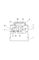
図1は、本発明による電子部品の一実施形態を示す模式断面図である。メモリキャパシタセル8(電子部品)は、拡散領域1A,1Bが形成されたシリコンウェハ1(基板)上に酸化膜から成るゲート絶縁膜2Bを介して設けられたゲート電極3(ワード線として機能する。)と、その上方に設けられた対向電極8Cとの間に二層構造の層間絶縁膜5,7(絶縁被膜)が形成されたものである。ゲート電極3の側壁には、側壁酸化膜4A、4Bが形成されており、また、ゲート電極の側方における拡散領域1Bにはフィールド酸化膜2Aが形成され、素子分離がなされている。
FIG. 1 is a schematic cross-sectional view showing an embodiment of an electronic component according to the present invention. The memory capacitor cell 8 (electronic component) functions as a gate electrode 3 (word line) provided via a
層間絶縁膜5は、これらのゲート電極3及びフィールド酸化膜2A上に被着されており、本発明のシリカ系被膜形成用組成物をスピンコートして形成されたものである。層間絶縁膜5におけるゲート電極3近傍にはビット線として機能する電極6が埋め込まれたコンタクトホール5Aが形成されている。さらに、平坦化された層間絶縁膜5上には平坦化された層間絶縁膜7が被着されており、両者を貫通するように形成されたコンタクトホール7Aには蓄積電極8Aが埋め込まれている。層間絶縁膜7は、層間絶縁膜5と同様に本発明のシリカ系被膜形成用組成物をスピンコートして形成されたものである。そして、蓄積電極8A上に高誘電体から成るキャパシタ絶縁膜8Bを介して対向電極8Cが設けられている。なお、層間絶縁膜5、7は同一の組成を有していても異なる組成を有していてもよい。
The
上記例示したような電子部品によれば、シリカ系被膜の比誘電率が従来に比して十分に低減されるので、信号伝搬における配線遅延時間を十分に短縮できると同時に高信頼性をも実現できる。また、電子部品の生産の歩留まり及びプロセス裕度の向上を図ることが可能となる。さらに、本発明のシリカ系被膜形成用組成物からなるシリカ系被膜の優れた上記特性により、高密度且つ高品位で信頼性に優れた電子部品を提供できる。 According to the electronic parts as exemplified above, the relative permittivity of the silica coating is sufficiently reduced compared to the conventional one, so that the wiring delay time in signal propagation can be sufficiently shortened and at the same time high reliability is realized. it can. It is also possible to improve the production yield and process margin of electronic parts. Furthermore, due to the excellent characteristics of the silica-based coating film comprising the composition for forming a silica-based coating film of the present invention, an electronic component having high density, high quality and excellent reliability can be provided.
以下、本発明の好適な実施例についてさらに詳細な説明するが、本発明はこれらの実施例に限定されるものではない。 Hereinafter, the preferred embodiments of the present invention will be described in more detail, but the present invention is not limited to these embodiments.
(実施例1)
<シリカ系被膜形成用組成物の作製>
テトラエトキシシラン154.6gとメチルトリエトキシシラン120.6gとをシクロヘキサノン543.3gに溶解させた溶液中に、70%硝酸0.525gを溶解させた水溶液80.98gを攪拌下で30分かけて滴下した。滴下終了後5時間反応させ、続いて、減圧下、温浴中で生成エタノール及びシクロヘキサノンの一部を留去して、ポリシロキサン溶液583.7gを得た。GPCによりポリシロキサンの重量平均分子量を測定したところ、1,350であった。
(Example 1)
<Preparation of a composition for forming a silica-based film>
In a solution prepared by dissolving 154.6 g of tetraethoxysilane and 120.6 g of methyltriethoxysilane in 543.3 g of cyclohexanone, 80.98 g of an aqueous solution in which 0.525 g of 70% nitric acid was dissolved was stirred for 30 minutes. It was dripped. After completion of the dropwise addition, the reaction was allowed to proceed for 5 hours. Subsequently, a portion of the produced ethanol and cyclohexanone was distilled off in a warm bath under reduced pressure to obtain 583.7 g of a polysiloxane solution. When the weight average molecular weight of the polysiloxane was measured by GPC, it was 1,350.
次いで、ポリシロキサン溶液553.9gに、空隙形成用化合物であるポリプロピレングリコール(アルドリッチ社製、PPG725)24.86g、シクロヘキサノン498.7g、2.38%のテトラメチルアンモニウム硝酸塩水溶液(PH3.6)17.89g、及び1%に希釈したマレイン酸水溶液5.5gをそれぞれ添加し室温で30分間攪拌溶解して、本発明のシリカ系被膜形成用組成物を作製した。なお、空隙形成用化合物として使用したポリプロピレングリコール(アルドリッチ社製、PPG725)の350℃における重量減少率は99.9%であった。 Subsequently, 24.86 g of polypropylene glycol (manufactured by Aldrich, PPG725) 24.86 g, cyclohexanone 498.7 g, and 2.38% tetramethylammonium nitrate aqueous solution (PH3.6) 17 were added to 553.9 g of the polysiloxane solution. .89 g and 5.5 g of a maleic acid solution diluted to 1% were added and stirred and dissolved at room temperature for 30 minutes to prepare the composition for forming a silica-based film of the present invention. In addition, the weight loss rate at 350 ° C. of polypropylene glycol (manufactured by Aldrich, PPG725) used as the void forming compound was 99.9%.
(実施例2)
テトラエトキシシラン154.6gとメチルトリエトキシシラン120.6gとをシクロヘキサノン543.3gに溶解させた溶液中に、70%硝酸0.525gを溶解させた水溶液80.98gを攪拌下で30分かけて滴下した。滴下終了後5時間反応させ、続いて、減圧下、温浴中で生成エタノールおよびシクロヘキサノンの一部を留去して、ポリシロキサン溶液598.2gを得た。GPC法によりポリシロキサンの重量平均分子量を測定したところ、1,280であった。
(Example 2)
In a solution prepared by dissolving 154.6 g of tetraethoxysilane and 120.6 g of methyltriethoxysilane in 543.3 g of cyclohexanone, 80.98 g of an aqueous solution in which 0.525 g of 70% nitric acid was dissolved was stirred for 30 minutes. It was dripped. After completion of the dropwise addition, the reaction was allowed to proceed for 5 hours. Subsequently, a portion of the produced ethanol and cyclohexanone was distilled off in a warm bath under reduced pressure to obtain 598.2 g of a polysiloxane solution. It was 1,280 when the weight average molecular weight of polysiloxane was measured by GPC method.
次いで、ポリシロキサン溶液514.5gに、空隙形成用化合物であるポリプロピレングリコール(アルドリッチ社製、PPG725)22.60g、ジエチレングリコールジメチルエーテル441.6g、2.38%のテトラメチルアンモニウム硝酸塩水溶液(PH3.6)16.26g、及び1%に希釈したマレイン酸水溶液5.0gをそれぞれ添加し室温で30分間攪拌溶解して、本発明のシリカ系被膜形成用組成物を作製した。なお、空隙形成用化合物として使用したポリプロピレングリコール(アルドリッチ社製、PPG725)の350℃における重量減少率は99.9%であった。 Next, 514.5 g of a polysiloxane solution was added to 22.60 g of polypropylene glycol (manufactured by Aldrich, PPG725), 441.6 g of diethylene glycol dimethyl ether, and a 2.38% tetramethylammonium nitrate aqueous solution (PH 3.6). 16.26 g and 5.0 g of a maleic acid solution diluted to 1% were added and dissolved by stirring for 30 minutes at room temperature to prepare the silica-based film forming composition of the present invention. In addition, the weight loss rate at 350 ° C. of polypropylene glycol (manufactured by Aldrich, PPG725) used as the void forming compound was 99.9%.
(比較例1)
テトラエトキシシラン154.6gとメチルトリエトキシシラン120.6gとをエタノール543.3gに溶解させた溶液中に、70%硝酸0.525gを溶解させた水溶液80.98gを攪拌下で30分かけて滴下した。滴下終了後5時間反応させて、ポリシロキサン溶液819.0gを得た。GPC法によりポリシロキサンの重量平均分子量を測定したところ、1,170であった。
(Comparative Example 1)
In a solution prepared by dissolving 154.6 g of tetraethoxysilane and 120.6 g of methyltriethoxysilane in 543.3 g of ethanol, 80.98 g of an aqueous solution in which 0.525 g of 70% nitric acid was dissolved was stirred for 30 minutes. It was dripped. After completion of dropping, the reaction was allowed to proceed for 5 hours to obtain 819.0 g of a polysiloxane solution. It was 1,170 when the weight average molecular weight of polysiloxane was measured by GPC method.
次いで、ポリシロキサン溶液774.0gに、空隙形成用化合物であるポリプロピレングリコール(アルドリッチ社製、PPG725)22.60g、エタノール182.1g、2.38%のテトラメチルアンモニウム硝酸塩水溶液(PH3.6)16.26g、及び1%に希釈したマレイン酸水溶液5.0gをそれぞれ添加し室温で30分間攪拌溶解してシリカ系被膜形成用組成物を作製した。なお、空隙形成用化合物として使用したポリプロピレングリコール(アルドリッチ社製、PPG725)の350℃における重量減少率は99.9%であった。 Next, 774.0 g of the polysiloxane solution was mixed with 22.60 g of polypropylene glycol (manufactured by Aldrich, PPG725), 182.1 g of ethanol, 2.38% tetramethylammonium nitrate aqueous solution (PH3.6) 16 as a void-forming compound. .26 g and 1 g of 1% diluted maleic acid aqueous solution 5.0 g were added and dissolved by stirring at room temperature for 30 minutes to prepare a silica-based film forming composition. In addition, the weight loss rate at 350 ° C. of polypropylene glycol (manufactured by Aldrich, PPG725) used as the void forming compound was 99.9%.
(実施例3)
<層間絶縁膜の製造>
実施例1〜2及び比較例1で得たシリカ系被膜形成用組成物をシリコンウェハ上に回転塗布して塗膜膜を形成した。なお、塗布膜の形成は、硬化後500±50nmの膜厚を有する被膜になるように回転数を調整した。次いで、塗布膜中の有機溶媒を250℃で3分かけて除去した後、O2濃度が100ppm前後にコントロールされた石英チューブ炉を用いて400℃で30分間かけて有機溶媒を除去した後の塗布膜を最終硬化し、層間絶縁膜としてのシリカ系被膜を製造した。そして、得られたシリカ系被膜上にHe−Neレーザー光を照射し、波長633nmにおける光照射により生じた位相差から求められる膜厚を、分光エリプソメータ(ガートナー社製;エリプソメータL116B)で測定した。
(Example 3)
<Manufacture of interlayer insulating film>
The composition for forming a silica-based film obtained in Examples 1 and 2 and Comparative Example 1 was spin-coated on a silicon wafer to form a coating film. In addition, rotation speed was adjusted so that the formation of a coating film might become a film which has a film thickness of 500 +/- 50nm after hardening. Next, after removing the organic solvent in the coating film at 250 ° C. over 3 minutes, the organic solvent was removed over 30 minutes at 400 ° C. using a quartz tube furnace in which the O 2 concentration was controlled to around 100 ppm. The coating film was finally cured to produce a silica-based film as an interlayer insulating film. And the film thickness calculated | required from the phase difference produced by the light irradiation in wavelength 633nm was measured with the spectroscopic ellipsometer (the Gartner company make; ellipsometer L116B) by irradiating He-Ne laser beam on the obtained silica type coating film.
次いで、シリカ系被膜上に真空蒸着装置を用いてAl金属を直径2mmの円で、厚さ約0.1μmになるように真空蒸着した。これにより、Al金属とシリコンウェハ(低抵抗率基板)との間にシリカ系被膜を配置する構造を有する層間絶縁膜が製造された。 Next, Al metal was vacuum-deposited on the silica-based coating using a vacuum deposition apparatus so as to have a thickness of about 0.1 μm in a circle having a diameter of 2 mm. As a result, an interlayer insulating film having a structure in which a silica-based film is disposed between an Al metal and a silicon wafer (low resistivity substrate) was manufactured.
[比誘電率測定]
得られた層間絶縁膜の電荷容量を、LFインピーダンスアナライザー(横河電機社製:HP4192A)に、誘電体テスト・フィクスチャー(横河電機製:HP16451B)を接続した装置を用いて、温度23℃±2℃、湿度40%±10%、使用周波数1MHzの条件で測定した。
[Specific permittivity measurement]
The charge capacity of the obtained interlayer insulating film was measured using a device in which a dielectric test fixture (Yokogawa Electric: HP16451B) was connected to an LF impedance analyzer (Yokogawa Electric: HP4192A) at a temperature of 23 ° C. The measurement was performed under conditions of ± 2 ° C., humidity 40% ± 10%, and operating frequency 1 MHz.
そして、電荷容量の測定値を下記式;
層間絶縁膜の比誘電率=3.597×10⁻²×電荷容量(pF)×層間絶縁膜の膜厚(μm)
に代入し、層間絶縁膜の比誘電率を算出した。なお、層間絶縁膜の膜厚は、上記シリカ系被膜の膜厚測定で得られた値を用いた。
And the measured value of the charge capacity is given by the following formula:
Dielectric constant of interlayer insulating film = 3.597 × 10 −2 × charge capacity (pF) × film thickness of interlayer insulating film (μm)
And the relative dielectric constant of the interlayer insulating film was calculated. In addition, the value obtained by the film thickness measurement of the said silica-type film was used for the film thickness of an interlayer insulation film.
[弾性率測定]
ナノインデンターSA2(DCM,MTS社製)を用いて(温度:23℃±2℃、周波数:75Hz、弾性率の測定範囲:層間絶縁膜厚の1/10以下で、押し込み深さで変動しない範囲)層間絶縁膜の弾性率を測定した。
[Elastic modulus measurement]
Using nanoindenter SA2 (DCM, manufactured by MTS) (temperature: 23 ° C. ± 2 ° C., frequency: 75 Hz, elastic modulus measurement range: 1/10 or less of interlayer insulation film thickness, does not vary with indentation depth Range) The elastic modulus of the interlayer insulating film was measured.
実施例3で得た層間絶縁膜の電気特性及び弾性率(膜強度)の測定結果を表1に示す。

1…シリコンウェハ(基板)、1A,1B…拡散領域、2A…フィールド酸化膜、2B…ゲート絶縁膜、3…ゲート電極、4A,4B…側壁酸化膜、5,7…層間絶縁膜(絶縁被膜)、5A,7A…コンタクトホール、6…ビット線、8…メモリセルキャパシタ(電子部品)、8A…蓄積電極、8B…キャパシタ絶縁膜、8C…対向電極。 DESCRIPTION OF SYMBOLS 1 ... Silicon wafer (substrate), 1A, 1B ... Diffusion region, 2A ... Field oxide film, 2B ... Gate insulating film, 3 ... Gate electrode, 4A, 4B ... Side wall oxide film, 5, 7 ... Interlayer insulating film (insulating film) 5A, 7A ... contact hole, 6 ... bit line, 8 ... memory cell capacitor (electronic component), 8A ... storage electrode, 8B ... capacitor insulating film, 8C ... counter electrode.
Claims (17)
R1 nSiX4−n …(1)
[式中、R1はH原子若しくはF原子、又はB原子、N原子、Al原子、P原子、Si原子、Ge原子若しくはTi原子を含む基、又は炭素数1〜20の有機基を示し、Xは加水分解性基を示し、nは0〜2の整数を示す。但し、nが2のとき、各R1は同一でも異なっていてもよく、nが0〜2のとき、各Xは同一でも異なっていてもよい。]、
で表される化合物を加水分解縮合して得られるシロキサン樹脂と、
(b)成分:少なくとも1種の非プロトン性溶媒を含む有機溶媒と、
(c)成分:オニウム塩と、
(d)成分:250〜500℃の加熱温度において熱分解又は揮発する空隙形成用化合物と、
を含有してなる、シリカ系被膜形成用組成物。 (A) component: the following general formula (1);
R 1 n SiX 4-n (1)
[Wherein R 1 represents an H atom or an F atom, or a group containing a B atom, an N atom, an Al atom, a P atom, a Si atom, a Ge atom or a Ti atom, or an organic group having 1 to 20 carbon atoms, X represents a hydrolyzable group, and n represents an integer of 0 to 2. However, when n is 2, each R 1 may be the same or different, and when n is 0 to 2, each X may be the same or different. ],
A siloxane resin obtained by hydrolytic condensation of a compound represented by:
(B) component: an organic solvent containing at least one aprotic solvent;
(C) component: onium salt,
(D) component: a void-forming compound that is thermally decomposed or volatilized at a heating temperature of 250 to 500 ° C .;
A composition for forming a silica-based film, comprising:
請求項1〜13のいずれか一項に記載のシリカ系被膜形成用組成物を基板上に塗布して塗布膜を形成し、該塗布膜に含まれる有機溶媒を除去した後、該塗布膜を250〜500℃の加熱温度で焼成することを特徴とするシリカ系被膜の形成方法。 A method of forming a silica-based film on a substrate,
The composition for forming a silica-based film according to any one of claims 1 to 13 is applied on a substrate to form a coating film, and after removing the organic solvent contained in the coating film, the coating film is formed. A method for forming a silica-based coating, comprising firing at a heating temperature of 250 to 500 ° C.
Priority Applications (1)
| Application Number | Priority Date | Filing Date | Title |
|---|---|---|---|
| JP2004302043A JP2005105281A (en) | 2004-10-15 | 2004-10-15 | Silicious film-forming composition, silicious film and its forming method, and electronic part having silicious film |
Applications Claiming Priority (1)
| Application Number | Priority Date | Filing Date | Title |
|---|---|---|---|
| JP2004302043A JP2005105281A (en) | 2004-10-15 | 2004-10-15 | Silicious film-forming composition, silicious film and its forming method, and electronic part having silicious film |
Related Parent Applications (1)
| Application Number | Title | Priority Date | Filing Date |
|---|---|---|---|
| JP2003068544A Division JP3674041B2 (en) | 2003-03-13 | 2003-03-13 | Composition for forming silica-based film, silica-based film and method for forming the same, and electronic component including silica-based film |
Publications (1)
| Publication Number | Publication Date |
|---|---|
| JP2005105281A true JP2005105281A (en) | 2005-04-21 |
Family
ID=34545232
Family Applications (1)
| Application Number | Title | Priority Date | Filing Date |
|---|---|---|---|
| JP2004302043A Withdrawn JP2005105281A (en) | 2004-10-15 | 2004-10-15 | Silicious film-forming composition, silicious film and its forming method, and electronic part having silicious film |
Country Status (1)
| Country | Link |
|---|---|
| JP (1) | JP2005105281A (en) |
Cited By (4)
| Publication number | Priority date | Publication date | Assignee | Title |
|---|---|---|---|---|
| US8557877B2 (en) | 2009-06-10 | 2013-10-15 | Honeywell International Inc. | Anti-reflective coatings for optically transparent substrates |
| US8864898B2 (en) | 2011-05-31 | 2014-10-21 | Honeywell International Inc. | Coating formulations for optical elements |
| US8901268B2 (en) | 2004-08-03 | 2014-12-02 | Ahila Krishnamoorthy | Compositions, layers and films for optoelectronic devices, methods of production and uses thereof |
| US10544329B2 (en) | 2015-04-13 | 2020-01-28 | Honeywell International Inc. | Polysiloxane formulations and coatings for optoelectronic applications |
-
2004
- 2004-10-15 JP JP2004302043A patent/JP2005105281A/en not_active Withdrawn
Cited By (5)
| Publication number | Priority date | Publication date | Assignee | Title |
|---|---|---|---|---|
| US8901268B2 (en) | 2004-08-03 | 2014-12-02 | Ahila Krishnamoorthy | Compositions, layers and films for optoelectronic devices, methods of production and uses thereof |
| US8557877B2 (en) | 2009-06-10 | 2013-10-15 | Honeywell International Inc. | Anti-reflective coatings for optically transparent substrates |
| US8784985B2 (en) | 2009-06-10 | 2014-07-22 | Honeywell International Inc. | Anti-reflective coatings for optically transparent substrates |
| US8864898B2 (en) | 2011-05-31 | 2014-10-21 | Honeywell International Inc. | Coating formulations for optical elements |
| US10544329B2 (en) | 2015-04-13 | 2020-01-28 | Honeywell International Inc. | Polysiloxane formulations and coatings for optoelectronic applications |
Similar Documents
| Publication | Publication Date | Title |
|---|---|---|
| JP4169088B2 (en) | Composition for forming silica-based film, silica-based film, method for producing the same, and electronic component | |
| JP3674041B2 (en) | Composition for forming silica-based film, silica-based film and method for forming the same, and electronic component including silica-based film | |
| US8466229B2 (en) | Composition for forming silica-based film, method of forming silica-based film, and electronic component provided with silica-based film | |
| JP2003064307A (en) | Silica-based film, composition for forming silica-based film, method for producing silica-based film and electronic part | |
| JP3966026B2 (en) | Silica-based film forming composition, silica-based film and method for producing the same, and electronic component | |
| JP4972834B2 (en) | Siloxane resin | |
| JP4110797B2 (en) | Composition for forming silica-based film, method for producing silica-based film, and electronic component | |
| JP3702842B2 (en) | Composition for forming silica-based film, silica-based film, method for producing silica-based film, and electronic component | |
| JP5143335B2 (en) | Composition for forming silica-based film, silica-based film and method for forming the same, and electronic component provided with silica-based film | |
| JP4110796B2 (en) | Composition for forming silica-based film, method for producing silica-based film, and electronic component | |
| JP5143334B2 (en) | Composition for forming silica-based film, silica-based film and method for forming the same, and electronic component provided with silica-based film | |
| JP2006045352A (en) | Silica film-forming composition, silica film, its forming method and electronic part having silica film | |
| JP2005072615A (en) | Silica-based film forming composition, silica-based film, method of manufacturing silica-based film, and electronic part | |
| JP2005136429A (en) | Silica coat formation composition, silica coat and its formation method, and electronic component having silica coat | |
| JP2004277508A (en) | Silica film-forming composition, silica film, its forming method and electronic part having silica film | |
| JP2008050610A (en) | Silicaceous film forming composition, silicaceous film, method for producing the same, and electronic component | |
| JP2005105281A (en) | Silicious film-forming composition, silicious film and its forming method, and electronic part having silicious film | |
| JP2005105283A (en) | Silicious film-forming composition, silicious film and its forming method, and electronic part having silicious film | |
| JP2005105282A (en) | Silicious film-forming composition, silicious film and its forming method, and electronic part having silicious film | |
| JP2005042118A (en) | Composition for forming silica-based coating film, manufacturing method for silica-based coating film, and electronic part | |
| JP2004277502A (en) | Silica film-forming composition, silica film, its forming method and electronic part having silica film | |
| JP2007291167A (en) | Composition for forming silica-based coating film, method for producing silica-based coating film and electronic component | |
| JP2005105284A (en) | Compositions for forming silica-based coating film, silica-based coating film and method of manufacturing silica-based coating film, and electronic parts | |
| JP2006055700A (en) | Method for forming silica based hardened coating film, liquid for improving silica based hardened coating film, silica based hardened coating film and electronic component | |
| JP3900915B2 (en) | Composition for forming silica-based film, method for producing silica-based film, and electronic component |
Legal Events
| Date | Code | Title | Description |
|---|---|---|---|
| A521 | Written amendment |
Free format text: JAPANESE INTERMEDIATE CODE: A523 Effective date: 20050131 |
|
| A761 | Written withdrawal of application |
Free format text: JAPANESE INTERMEDIATE CODE: A761 Effective date: 20050315 |