JP2004507020A - Modular memory devices - Google Patents
Modular memory devices Download PDFInfo
- Publication number
- JP2004507020A JP2004507020A JP2002520233A JP2002520233A JP2004507020A JP 2004507020 A JP2004507020 A JP 2004507020A JP 2002520233 A JP2002520233 A JP 2002520233A JP 2002520233 A JP2002520233 A JP 2002520233A JP 2004507020 A JP2004507020 A JP 2004507020A
- Authority
- JP
- Japan
- Prior art keywords
- memory
- digital
- support element
- unit
- interface unit
- Prior art date
- Legal status (The legal status is an assumption and is not a legal conclusion. Google has not performed a legal analysis and makes no representation as to the accuracy of the status listed.)
- Pending
Links
Images

Classifications
-
- G—PHYSICS
- G11—INFORMATION STORAGE
- G11C—STATIC STORES
- G11C5/00—Details of stores covered by group G11C11/00
- G11C5/02—Disposition of storage elements, e.g. in the form of a matrix array
- G11C5/025—Geometric lay-out considerations of storage- and peripheral-blocks in a semiconductor storage device
-
- G—PHYSICS
- G11—INFORMATION STORAGE
- G11C—STATIC STORES
- G11C5/00—Details of stores covered by group G11C11/00
- G11C5/06—Arrangements for interconnecting storage elements electrically, e.g. by wiring
- G11C5/063—Voltage and signal distribution in integrated semi-conductor memory access lines, e.g. word-line, bit-line, cross-over resistance, propagation delay
Abstract
Description
【0001】
【技術分野】
本発明は、不揮発性ソリッドステートメモリアレーを含むモジュラーメモリデバイスに係る。
【0002】
【背景技術】
種々のポータブル型消費者製品は、デジタルデータを捕獲して不揮発式に記憶する。デジタルカメラ及びデジタルオーディオプレーヤは、このような製品の2つの例である。この種の製品のメモリデバイスは、手のひらに載るに充分なほど小さくそしてユーザにより搬送容易なモジュラー装置であるのが好ましい。理想的には、これら記憶装置は、取り外し可能で且つ軽量でなければならず、そして数メガバイトの記憶容量を与えると共に低い実販売価格(ASP)を達成しなければならない。
【0003】
このようなメモリデバイスに対する1つの公知の解決策は、フラッシュメモリカードとして知られている。このようなカードは、ユーザの手のひらにフィットし、軽量であり、そして消費者市場のポータブル装置部門のニーズにマッチする記憶容量を与える。しかしながら、フラッシュメモリカードは、この市場部門のコスト要求に充分応えるものではない。コンパクトフラッシュ(登録商標)カードのようなフラッシュメモリカードに対する2000年6月現在のメガバイト当たりのコストは、40メガバイトレベルで$2ないし4(ASP)である。市場のポータブル装置部門におけるほとんどの消費者向けアプリケーションは、少なくとも40メガバイトの不揮発性記憶を必要とするので、フラッシュメモリカードは、装置全体のコストの顕著な部分を占める。
【0004】
この市場部門に向けて製造される他のメモリカードは、マルチメディアカード(MMC)を含み、その2000年6月現在のメガバイト当たりのコストは、$3ないし5(ASP)である。これらメモリカードは、全て、従来の二次元メモリアレーを使用している。
【0005】
【発明の開示】
以下に述べる好ましい実施形態は、不揮発性デジタル記憶を要求する消費者アプリケーションのサイズ、重量、記憶及びコスト要件を満足するものである。これらの実施形態は、支持素子により支持されたメモリアレー及びメモリアレーコントローラと、支持素子により支持されてメモリアレーコントローラに接続された電気コネクタとを備えている。メモリアレーは、現場でプログラム可能な(フィールドプログラマブルな)一度書き込みの三次元メモリアレーであるのが好ましいが、必ずしもそうでなくてもよい。このようなメモリアレーは、ビット当たりのコストが実質的に減少されるという利点を発揮する。デバイスインターフェイスユニットが使用されるときには、コストを最小にするためにそれが高度に一体化されるのが好ましい。メモリユニット及びデバイスインターフェイスユニットの両方のコストを減少することにより、モジュラーメモリデバイスの全体的なコストが、上述した公知技術に比して実質的に減少される。
このセクションは、一般的な導入部として設けられたもので、特許請求の範囲を何ら限定するものではない。
【0006】
【発明を実施するための最良の形態】
添付図面を参照すれば、図1は、電気コネクタ12を一端に備えたモジュラーメモリデバイス10の全体図である。メモリデバイス10の外面は、図示されたようにハウジング13内に包囲される。ハウジング13は、デバイス10の内部部品を保護し、そして消費者により容易に搬送され且つカメラや電子ブックのような読み取り/書き込み装置に容易に挿入及び除去されるコンパクトなモジュラーハンドヘルドユニットを形成する。コネクタ12は、いかなる適当な形態をとることもでき、この例では、一連の導電性パッドとして構成され、これらパッドは、相手コネクタ(図示せず)の対応コンタクトと嵌合するように離間配置される。もちろん、いかなる適当なコネクタ12を使用することもでき、本発明は、図1に示されたエッジコネクタに限定されない。
【0007】
図2は、図1のデバイス10の断面図である。図2に示すように、デバイス10は、この実施形態ではプリント回路板14の形態をとる支持素子を備えている。プリント回路板14は、デバイス10の外面の1つを形成してもよい。プリント回路板14は、メモリユニット16、デバイスインターフェイスユニット18及び電気コネクタ12を支持する。
【0008】
メモリユニット16は、三次元メモリアレー及びそれに関連したメモリアレーコントローラを含むのが好ましい。好ましいメモリアレーは、基体上に三次元格子に配列された適当な数のメモリセルを含む。ジョンソン氏の米国特許第6,034,882号、クナル氏の米国特許出願第09/560,626号及びジョンソン氏の米国特許出願第09/638,428号に開示された三次元メモリを、メモリアレーとして使用することができる。これら特許文献は、全て、本発明の譲受人に譲渡されたもので、参考としてここに援用する。メモリアレーコントローラは、メモリアレーが形成される同じ基体上に形成されるのが好ましく、そしてメモリアレーコントローラは、アドレスデコード回路、読み取り動作のための感知回路、書き込み動作のためのドライブ回路、及びI/O増幅器を含むI/Oインターフェイス回路を備えている。
【0009】
この実施形態のデバイスインターフェイスユニット18は、個別の基体に形成され、そしてプリント回路板14を経てメモリユニット16及び電気コネクタ12に電気的接続される。この実施形態では、メモリユニット16及びデバイスインターフェイスユニット18は、プリント回路板に直接取り付けられる。デバイスインターフェイスユニット18は、シリコン基体の単一片に全てが集積される種々の消費者装置にメモリデバイス10を取り付けられるようにする電圧、クロック周波数及びプロトコルロジックを形成するのに必要な全ての部品を備えている。1つの実施形態では、デバイスインターフェイスユニット18は、使用するプロトコル(例えば、コンパクトフラッシュプロトコルのようなプロトコル)に含まれるタスクファイル、割り込み管理、エラーレポート及びコンフィギュレーションファンクションを実施するための回路(ハードウェア、ソフトウェア及びファームウェアの適当な組合せを使用する)を備えている。
【0010】
図3は、図2の実施形態の変形を示す。図3の実施形態では、デバイスインターフェイスユニット18及びメモリユニット16は、この分野で知られたTSOP又はTQFPパッケージのような従来の中間チップパッケージに梱包される。これらのパッケージされた素子は、次いで、従来のやり方でプリント回路板14に組み立てられる。
【0011】
図4の実施形態では、三次元メモリアレー、メモリアレーコントローラ及びデバイスインターフェイスユニットが単一基体20に製造され、これが、中間パッケージをもたずにプリント回路板14に直接取り付けられるのが好ましい。メモリアレーコントローラ及びデバイスインターフェイスユニットは、三次元メモリアレーの下でシリコン基体に製造することができる。この構成は、メモリデバイスの製造コストを減少する。この場合に、メモリアレーコントローラは、上述したI/O増幅器を必要としない。
【0012】
図4の実施形態は、コンパクトフラッシュプロトコルを使用するもののようなアプリケーションに良く適している。この実施形態は、不揮発性メモリセルの二次元又は三次元メモリアレーで実施することができる。
最低コストのコントローラを形成するために、メモリユニット16を所望の標準メモリカードにインターフェイスするのに必要な信号の合計数が決定される。シリコンチップ内部の電源システムを、あらゆる動作条件の下で欠陥のない動作を保証するに充分なほど安定した状態に保持するに必要な電力及び接地接続の数が、次いで、このリストに加えられる。このピンカウント情報は、必要な接続の数を収容する最小の長方形を決定する。この長方形の大きさは、ピン数の1/4と、ピン駆動回路の高さ及び巾の関数である。その結果生じるエッジの長さは、次の式で表わされる。
長さ=(ピン数/4)×ピン駆動回路の巾+2×ピン駆動回路の高さ
ダイ面積=長さ2
【0013】
この長さの式が最小にされると、必要なダイ面積がセットされる。次いで、メモリユニット16を選択された標準システムバスに接続するのに必要な所要のロジック機能及び所要の電力又はクロック回路を形成するのに使用可能な面積を、次の式により決定することができる。
使用可能な面積=((ピン数/4)×ピン駆動回路の巾)2
次いで、必要なコンポーネントの数をコンポーネントの密度で除算したものが上記式の使用可能な面積の計算値に等しくなるように、適当なロジック密度を与えるシリコンプロセス技術が選択される。
【0014】
上記実施形態では、メモリセルが二次元ではなく三次元に編成されそして形成される。メモリセルの層は多数あり、これらの層は、垂直方向に互いに上下にスタックされる。3つの次元は、「行」、「列」及び「層」と称される。典型的に、行及び列は、その下の基体の上面に一般的に平行であり、そして層は、その下の基体の上面に垂直な方向に沿って互いに離間される。
あるメモリセルは、上方又は下方のいずれかに突出する素子を含み、過去において、「三次元メモリセル」と称されている。しかしながら、これらのメモリセルは、従来の二次元アレーに配列される。これは、メモリセルの多数の層が垂直方向に互いに上下にスタックされたメモリセルの三次元アレーを含むここに開示する三次元実施形態とはかなり相違する。
【0015】
これら実施形態の顕著な特徴は、低コスト三次元編成であることの代わりに、メモリの動作速度を明らかに低下させることである。これら実施形態は、小さなメモリセル及び小さな全チップ面積が与えられると、非常に小さなスイッチングデバイスを使用する。又、小さなスイッチングデバイスは、小さな読み取り電流を与え、これは、読み取りアクセス時間を比較的低速にする。しかしながら、低速のアクセス時間を容易に許容し、そして劇的に安いメモリのコストから多大な利益を引き出す重要なメモリアプリケーションが多数ある。これら低速アプリケーションの多くは、「デジタル媒体記憶」という名の下に集合され、そして次のものを含む。即ち、写真のような静止像のデジタル記憶、音楽及び一般にデジタルオーディオのデジタル記憶、デジタルブック、マップのデジタル記憶、デジタルビデオを含む像のシーケンス、及び当業者に容易に明らかな多数の他の例。デジタル媒体記憶アプリケーションは、版権取得できる資料を有形の表現媒体に固定できるようにする記憶アプリケーションとみなすことができる。このようなアプリケーションの場合、記憶媒体を再書き込みできることは、利点ではなく、実際には、不所望なことすらある。例えば、表現された資料の明確で且つ不変の記録をもつことが重要である。更に、再書き込み可能なメモリデバイスよりも一度書き込みの方がコストは一般的に低い。
【0016】
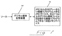
図7は、デジタル媒体記憶装置30と組み合わせて上記メモリデバイス10をブロック図の形態で示す。メモリデバイス10は、ここに述べるいかなる形式をとることもでき、そして現場でプログラム可能な一度書き込みのメモリセルの3Dアレーを含むのが好ましい。上述したように、このようなデバイスは、著しく低コストであるという利点を与える。メモリデバイス10は、ユーザがこのメモリデバイス10をデジタル媒体記憶装置30に容易に接続したり取り外したりできるようにする上述した外部コネクタを伴うモジュラーハンドヘルドユニットとして形成される。メモリデバイス10の構造に関する更なる詳細は、米国特許出願第09/638,439号及び第09/638,427号に開示されており、これらは両方とも、本出願と同日に出願され、本発明の譲受人に譲渡され、そしてその全体を参考としてここに援用するものである。別の実施形態においては、米国特許出願第09/639,702号及び第09/639,577号に開示されたような多数書き込み3Dアレーが使用され、これら出願も、本出願と同日に出願され、そして本発明の譲受人に譲渡されたものである。
【0017】
デジタル媒体記憶装置30は、いかなる適当な形態をとることもでき、そして例えば、デジタルカメラ、デジタルオーディオ再生装置、又は電子ブックである。この記憶装置30は、2つの個別の機能を遂行する。第1に、記憶装置30は、例えば、静止像又は移動像を示すか、オーディオファイルを再生するか、又は電子ブックのページを表示することにより、メモリデバイス10に記憶されたデジタル媒体をユーザに表示する。第2に、記憶装置30は、メモリデバイス10を所望のデジタル媒体情報で現場でプログラムするように使用できる。このため、デジタル媒体記憶装置30は、ソースに接続され、そしてソースからメモリデバイス10へデジタル媒体情報を現場でプログラムする。デジタル媒体ソースは、いかなる適当な形態をとることもでき、そして別のコンピュータ(図示せず)をしばしば含む。例えば、ソースは、インターネットのようなネットワークを経て或いはレコード店や書店のような店舗に設けられたシステムを経て記憶装置30へデジタル媒体情報を供給し、消費者が所持するメモリデバイス10にデジタル媒体をダウンロードすることができる。又、デジタルデータのソースは、デジタルカメラの場合のように電荷結合装置アレー(CCD)の出力、又は音楽再生−記録装置の場合のようにコーダ−デコーダ(CODEC)の出力を含んでもよいが、これに限定されない。あるアプリケーションでは、ソースは、デジタル媒体記憶装置30を経てではなく直接的にメモリデバイス10にデジタル媒体情報を記憶してもよく、これは、現場でプログラム可能であることの別の例である。一般的に、「現場でプログラム可能(フィールドプログラマブル)」という語は、メモリデバイスの製造が完了した後の時間にユーザにより選択されたファイルをメモリデバイスに書き込むことも包含すると広く解釈される。
【0018】
ここに説明する実施形態のメモリアレーは、メモリセルの多数の層の垂直スタックを備え、メモリセルは、いかなる所望の形態をとることもでき、ツアン氏の米国特許第5,835,396号、ジョンソン氏の米国特許第6,034,882号及びクナル氏の米国特許出願第09/560,626号に教示されたメモリセルが一例として取り上げられる。しかしながら、ここに述べる好ましい実施形態は、コストを最小にするように設計されており、それ故、メモリセルは、できるだけ小さくされる。
【0019】
メモリセルを小さくするために、微細ピッチのホトリソグラフィーを使用してメモリセルの幾何学的形状がパターン化される。より詳細には、ワード線及びビット線は、約1ミクロン以下の線巾及び約1ミクロン以下の線−線間隔で形成されるのが好ましい。これらF(ホトリソグラフィック特徴サイズ)の値は、更に減少されてもよく、即ち、線巾及び間隔は、約0.25ミクロンより小さいのが更に好ましい。
【0020】
図5は、上述した形式のメモリアレーの一実施形態を示す概略図である。メモリセルMC1、MC2の各々は、状態記憶素子を含む2端子セルである。この実施形態では、メモリセルMC1は、第1レベルに配置され、そしてメモリセルMC2は、第1レベルに対して垂直方向にスタックされた第2レベルに配置される。メモリセルMC1、MC2の端子は、セルの各端に配置される。この点について、「端子」という語は、広く解釈されるべきであり、そして端子は、単にセルの端子部分として実施されてもよいし又はセルの個別層として実施されてもよい。
【0021】
各メモリセルMC1、MC2の各端子は、各導体又はワイヤと電気的接触する。図5において、メモリセルMC1の下部の導体W1、W2は、ワード線として構成され、そしてメモリセルMC1の上部端子に接続された導体B1、B2は、ビット線として構成され、これらのビット線は、この実施形態では、ワード線W1、W2に実質的に垂直に延びる。従って、メモリセルMC1の各々は、ワード線W1、W2の選択されたものと、ビット線B1、B2の選択されたものをブリッジ接続する。
【0022】
同様に、第2層のメモリセルMC2は、ビット線B1、B2の選択されたものと、ワード線W3、W4の選択されたものとの間に接続される。この実施形態のワード線W3、W4は、垂直方向にビット線B1、B2のレベルより上にスタックされた別のレベルに配置される。
図5のメモリセルアレーは、基本的な幾何学形状及び材料が、上記ジョンソン氏の特許の図6aないし6gに示されたものと同様でよい。
【0023】
平面図での基本的セルサイズが2Fx2Fである実施形態の場合(上記ジョンソン氏及びクナル氏の特許文献に教示されたような)、メモリセルのピッチ(100個の隣接セルの全巾を100で除算した)は、ワード線又はビット線の方向に約0.50ミクロン以下(及び一般的には2ミクロン以下)であるのが好ましく、そしてメモリセルにより消費される全面積は、約0.25平方ミクロン以下であるのが好ましい。従って、消費されるチップ面積は、垂直スタックの各層において百万ビット当たり約0.25平方ミリメーター以下である。同じ結果を別の言い方で述べると、パッキング密度が、垂直スタックの各層において平方ミリメーター当たり4百万ビット以上である。
【0024】
垂直方向にスタックすると、所与のサイズのメモリアレーに対して密度が高くなりそしてチップ面積が減少し、即ち8層のメモリセルが垂直方向に互いに上下に積層された好ましい実施形態では、密度が、チップ面積1平方ミリメーター当たり3千2百万ビット以上となる。
微細ピッチのリソグラフィーが改善されるので、これらのメモリセルの密度も改善される。次の式は、特徴サイズがFのリソグラフィー世代の場合であって、2Fx2FセルのN層が垂直にスタックされた場合に、単位面積当たりのパッキング密度(ビット)を示している。
パッキング密度=N/(4F2)
【0025】
パッキング密度が低い本発明の他の実施形態は、4F2より大きなメモリセル(例えば、上記ツアン氏の特許の図6Bに示されたメモリセルを参照されたい)を使用できることに注意されたい。これらの大きなメモリセルは、チップ面積が大きくなり、従って、あまり望ましくない。
デバイスインターフェイスユニット18の好ましい実施形態が図6にブロック図で示されている。この例では、コンパクトフラッシュインターフェイス状態マシンが、コンパクトフラッシュプロトコルに対するタスクファイル、割り込み管理、エラーレポート、及びコンフィギュレーションファンクションを実施し、そしてスマートメディアインターフェイス状態マシンが、スマートメディアプロトコルに対するこれらの機能を実施する。これらの両プロトコルは、当業者に容易に入手できる。図6のデバイスインターフェイスユニットは、大きさが2.68mmx2.68mmで、7.18mm2の全基体面積を与えるシリコンダイに形成することができる。1つの実施形態では、上述したモジュラーメモリデバイス10を使用して、デジタル媒体、例えば、上記のいずれかのデジタル媒体が記憶される。
【0026】
別の実施形態では、デバイスインターフェイスユニット18がデバイス10から削除され、そしてメモリユニット16のメモリアレーコントローラがプリント回路板14によりコネクタ12に直接接続される。この場合に、メモリユニット16は、ホストシステムのデバイスインターフェイスユニットによって制御される。
上記実施形態は、3Dメモリアレーに向けられたが、別のコスト節減実施形態は、一回プログラム式(OTP)アレーを使用することに向けられる。例えば、電子的にプログラム可能なリードオンリメモリ(PROM)を使用することができる。このようなOTPメモリと、従来のE2PROM及びフラッシュメモリとの間のコストの差は、相当のものである。
【0027】
3Dの一回プログラム式、3Dの多数書き込み、又は2DのOTPの場合に、種々のハウジング材料及びコンフィギュレーションのいずれを使用することもできる。適当な材料は、金属、エポキシ、セラミック、及びプラスチックである。コンフィギュレーションは、従来、フラッシュメモリ又はE2PROMメモリと共に使用されていた標準的モジュールに適合するもの、又は将来開発される規格に適合するものを含む。これらは、コンパクトフラッシュ、スマートメディア、マルチメディアカード、セキュアデジタルミュージックイニシエーティブ(SDMI)、ソニーメモリステッィク及び他の規格を含むが、これらに限定されない。コンフィギュレーションは、個別又は非一体化のデバイスインターフェイスユニットを含むことができる(即ち、デバイスインターフェイスユニットは、設計上の選択の問題としてメモリユニットチップと一体化されてもよいし又はされなくてもよい)。モジュールは、パッケージされたダイの周りに形成することもできるし、又は各ダイを基体上に直接取り付け、次いで、基体をハウジング内にカプセル封入することもできる。基体は、シリコン、ファイバーガラス又はセラミックであるが、これらに限定されない。
【0028】
以上の説明から、低いコストで製造することができ、小型で且つ軽量であり、そして不揮発性メモリの必要な容量を与える改良されたモジュラーメモリデバイスが提供されたことが明らかであろう。
ここで使用した「接続」という語は、直接的に接続される素子及び間接的に接続される素子を含むものと広く解釈されたい。従って、互いに接続される2つの素子は、介在する無名の素子によって接続されてもよい。
【0029】
以上の詳細な説明は、本発明がとり得る多数の形態の若干を説明したに過ぎない。このため、この詳細な説明は、例示に過ぎず、これに限定されるものではない。全ての等効物を包含する特許請求の範囲のみが本発明の範囲を規定する。
【図面の簡単な説明】
【図1】本発明の好ましい実施形態によるモジュラーメモリデバイスの斜視図である。
【図2】図1のメモリデバイスの断面図である。
【図3】図1のメモリデバイスの別の実施形態の断面図である。
【図4】図1のメモリデバイスの別の実施形態の断面図である。
【図5】三次元メモリアレーの一部分を示す概略図である。
【図6】図2のデバイスインターフェイスユニット18の好ましい実施形態を示す回路図である。
【図7】デジタル媒体記憶システムに接続されたモジュラーメモリデバイスのブロック図である。[0001]
【Technical field】
The present invention relates to a modular memory device including a non-volatile solid state memory array.
[0002]
[Background Art]
Various portable consumer products capture and store digital data in a non-volatile manner. Digital cameras and digital audio players are two examples of such products. The memory device of this type of product is preferably a modular device that is small enough to fit on the palm and is easier to carry by the user. Ideally, these storage devices should be removable and lightweight, and should provide a few megabytes of storage capacity while achieving a low actual selling price (ASP).
[0003]
One known solution to such a memory device is known as a flash memory card. Such a card fits in the palm of a user's hand, is lightweight, and provides storage capacity that matches the needs of the portable devices sector of the consumer market. However, flash memory cards do not adequately meet the cost requirements of this market sector. The cost per megabyte as of June 2000 for a flash memory card, such as a CompactFlash card, is $ 2 to 4 (ASP) at the 40 megabyte level. Since most consumer applications in the portable device segment of the market require at least 40 megabytes of non-volatile storage, flash memory cards represent a significant portion of the overall device cost.
[0004]
Other memory cards manufactured for this market segment include multimedia cards (MMC), whose cost per megabyte as of June 2000 is $ 3 to 5 (ASP). All of these memory cards use a conventional two-dimensional memory array.
[0005]
DISCLOSURE OF THE INVENTION
The preferred embodiments described below satisfy the size, weight, storage and cost requirements of consumer applications requiring non-volatile digital storage. These embodiments include a memory array and a memory array controller supported by a support element, and an electrical connector supported by the support element and connected to the memory array controller. The memory array is preferably, but not necessarily, a field-programmable (field-programmable) write-once three-dimensional memory array. Such a memory array offers the advantage that the cost per bit is substantially reduced. When a device interface unit is used, it is preferably highly integrated to minimize costs. By reducing the cost of both the memory unit and the device interface unit, the overall cost of the modular memory device is substantially reduced as compared to the prior art described above.
This section is provided as a general introduction and does not limit the scope of the claims in any way.
[0006]
BEST MODE FOR CARRYING OUT THE INVENTION
Referring to the accompanying drawings, FIG. 1 is an overall view of a
[0007]
FIG. 2 is a cross-sectional view of the
[0008]
Memory unit 16 preferably includes a three-dimensional memory array and an associated memory array controller. Preferred memory arrays include a suitable number of memory cells arranged in a three-dimensional lattice on a substrate. The three-dimensional memory disclosed in Johnson, U.S. Pat. No. 6,034,882, Kunal, U.S. Ser. No. 09 / 560,626, and Johnson, U.S. Pat. Can be used as an array. All of these patents are assigned to the assignee of the present invention and are hereby incorporated by reference. The memory array controller is preferably formed on the same substrate on which the memory array is formed, and the memory array controller includes an address decode circuit, a sense circuit for a read operation, a drive circuit for a write operation, and an I / O circuit. An I / O interface circuit including an / O amplifier is provided.
[0009]
The device interface unit 18 of this embodiment is formed on a separate substrate and is electrically connected to the memory unit 16 and the electrical connector 12 via the printed circuit board 14. In this embodiment, the memory unit 16 and the device interface unit 18 are mounted directly on a printed circuit board. The device interface unit 18 contains all the components necessary to form the voltage, clock frequency and protocol logic that allow the
[0010]
FIG. 3 shows a variant of the embodiment of FIG. In the embodiment of FIG. 3, the device interface unit 18 and the memory unit 16 are packaged in a conventional intermediate chip package, such as a TSOP or TQFP package known in the art. These packaged components are then assembled to printed circuit board 14 in a conventional manner.
[0011]
In the embodiment of FIG. 4, the three-dimensional memory array, memory array controller and device interface unit are preferably fabricated on a single substrate 20, which is mounted directly to printed circuit board 14 without an intermediate package. The memory array controller and device interface unit can be manufactured on a silicon substrate under a three-dimensional memory array. This configuration reduces the manufacturing cost of the memory device. In this case, the memory array controller does not require the above-described I / O amplifier.
[0012]
The embodiment of FIG. 4 is well suited for applications such as those using the compact flash protocol. This embodiment can be implemented in a two-dimensional or three-dimensional memory array of non-volatile memory cells.
To form the lowest cost controller, the total number of signals required to interface memory unit 16 to the desired standard memory card is determined. The number of power and ground connections needed to keep the power system inside the silicon chip stable enough to ensure defect-free operation under all operating conditions is then added to this list. This pin count information determines the smallest rectangle that will contain the required number of connections. The size of this rectangle is a function of 1/4 of the number of pins and the height and width of the pin drive circuit. The length of the resulting edge is given by:
Length = (number of pins / 4) × width of pin drive circuit + 2 × height of pin drive circuit Die area = length 2
[0013]
When this length equation is minimized, the required die area is set. The required logic functions required to connect the memory unit 16 to the selected standard system bus and the area available to form the required power or clock circuitry can then be determined by the following equation: .
Usable area = ((number of pins / 4) × width of pin drive circuit) 2
A silicon process technique that provides the appropriate logic density is then selected such that the number of components required divided by the density of the components equals the calculated available area in the above equation.
[0014]
In the above embodiment, the memory cells are organized and formed in three dimensions rather than two dimensions. There are many layers of memory cells, and these layers are stacked one on top of the other in the vertical direction. The three dimensions are called "row", "column", and "layer". Typically, the rows and columns are generally parallel to the top surface of the underlying substrate, and the layers are spaced apart from each other along a direction perpendicular to the top surface of the underlying substrate.
Some memory cells include elements that protrude either upward or downward, and have been referred to in the past as "three-dimensional memory cells." However, these memory cells are arranged in a conventional two-dimensional array. This is significantly different from the disclosed three-dimensional embodiment, which includes a three-dimensional array of memory cells in which multiple layers of memory cells are vertically stacked on top of each other.
[0015]
The salient feature of these embodiments is that instead of having a low cost three-dimensional organization, the operating speed of the memory is significantly reduced. These embodiments use very small switching devices given small memory cells and small total chip area. Also, a small switching device provides a small read current, which makes the read access time relatively slow. However, there are a number of important memory applications that easily allow for slow access times and derive significant benefits from the cost of dramatically lower memory. Many of these slow applications are grouped under the name "Digital Media Storage" and include: That is, digital storage of still images, such as photographs, digital storage of music and generally digital audio, digital books, digital storage of maps, sequences of images including digital video, and numerous other examples readily apparent to those skilled in the art. . Digital media storage applications can be considered storage applications that allow copyrightable material to be secured to tangible media. For such applications, being able to rewrite the storage medium is not an advantage, and in fact, may even be undesirable. For example, it is important to have a clear and immutable record of the represented material. Furthermore, once-write is generally less expensive than re-writable memory devices.
[0016]
FIG. 7 shows the
[0017]
The digital
[0018]
The memory array of the embodiments described herein comprises a vertical stack of multiple layers of memory cells, the memory cells can take any desired form, and U.S. Pat. No. 5,835,396 to Tsuan, The memory cells taught in Johnson US Pat. No. 6,034,882 and Kunal US patent application Ser. No. 09 / 560,626 are taken as examples. However, the preferred embodiments described herein are designed to minimize cost, and therefore, the memory cells are made as small as possible.
[0019]
To make the memory cell smaller, the geometry of the memory cell is patterned using fine pitch photolithography. More specifically, the word lines and bit lines are preferably formed with a line width of about 1 micron or less and a line-to-line spacing of about 1 micron or less. These values of F (photolithographic feature size) may be further reduced, i.e., the line width and spacing are more preferably less than about 0.25 microns.
[0020]
FIG. 5 is a schematic diagram illustrating one embodiment of a memory array of the type described above. Each of the memory cells MC1 and MC2 is a two-terminal cell including a state storage element. In this embodiment, memory cell MC1 is located at a first level, and memory cell MC2 is located at a second level that is stacked vertically with respect to the first level. The terminals of the memory cells MC1, MC2 are arranged at each end of the cell. In this regard, the term "terminal" is to be interpreted broadly, and the terminal may be implemented simply as a terminal part of the cell or as an individual layer of the cell.
[0021]
Each terminal of each memory cell MC1, MC2 makes electrical contact with each conductor or wire. In FIG. 5, the lower conductors W1, W2 of the memory cell MC1 are configured as word lines, and the conductors B1, B2 connected to the upper terminal of the memory cell MC1 are configured as bit lines, and these bit lines are In this embodiment, the word lines extend substantially perpendicular to the word lines W1 and W2. Therefore, each of the memory cells MC1 bridges the selected one of the word lines W1, W2 and the selected one of the bit lines B1, B2.
[0022]
Similarly, the second-layer memory cell MC2 is connected between a selected one of the bit lines B1 and B2 and a selected one of the word lines W3 and W4. The word lines W3, W4 of this embodiment are arranged at another level vertically stacked above the levels of the bit lines B1, B2.
The memory cell array of FIG. 5 may be similar in basic geometry and materials to those shown in FIGS. 6a-6g of the Johnson patent.
[0023]
For embodiments where the basic cell size in plan view is 2Fx2F (as taught in the above-cited Johnson and Kunal patents), the pitch of the memory cells (the total width of 100 adjacent cells is 100 Is preferably less than about 0.50 microns (and typically less than 2 microns) in the direction of the word lines or bit lines, and the total area consumed by the memory cells is less than about 0.25 microns. It is preferably less than square microns. Thus, the chip area consumed is less than about 0.25 square millimeters per million bits in each layer of the vertical stack. Stated differently, the same result is that the packing density is 4 million bits or more per square millimeter in each layer of the vertical stack.
[0024]
Vertical stacking increases density and reduces chip area for a given size memory array, i.e., in a preferred embodiment where eight layers of memory cells are stacked vertically one above the other, the density is reduced. And more than 32 million bits per square millimeter of chip area.
As fine pitch lithography is improved, the density of these memory cells is also improved. The following equation shows the packing density (bits) per unit area when the feature size is F in the lithography generation and the N layers of the 2Fx2F cell are vertically stacked.
Packing density = N / (4F 2 )
[0025]
Other embodiments of the packing density is low the present invention it is noted that the use of larger memory cell than 4F 2 (see, eg, memory cell shown in Figure 6B of the patent says the Tsuan). These large memory cells have a large chip area and are therefore less desirable.
A preferred embodiment of the device interface unit 18 is shown in a block diagram in FIG. In this example, the CompactFlash interface state machine implements task files, interrupt management, error reporting, and configuration functions for the CompactFlash protocol, and the SmartMedia interface state machine implements these functions for the SmartMedia protocol. . Both of these protocols are readily available to those skilled in the art. The device interface unit of FIG. 6 can be formed on a silicon die that measures 2.68 mm × 2.68 mm and provides a total substrate area of 7.18 mm 2 . In one embodiment, digital media, such as any of the above, is stored using the
[0026]
In another embodiment, the device interface unit 18 is deleted from the
While the above embodiment was directed to a 3D memory array, another cost saving embodiment is directed to using a one time programmable (OTP) array. For example, an electronically programmable read only memory (PROM) can be used. The cost difference between such OTP memory and conventional E 2 PROM and flash memory is substantial.
[0027]
In the case of 3D one-time programming, 3D multiple writing, or 2D OTP, any of a variety of housing materials and configurations can be used. Suitable materials are metals, epoxies, ceramics, and plastics. Configuration, including conventional, shall conform to standard modules that have been used in conjunction with flash memory or E 2 PROM memory, or one to meet future development performance limits. These include, but are not limited to, compact flash, smart media, multimedia cards, Secure Digital Music Initiative (SDMI), Sony Memory Stick and other standards. The configuration may include individual or non-integrated device interface units (ie, the device interface units may or may not be integrated with the memory unit chip as a matter of design choice). ). The module can be formed around a packaged die, or each die can be mounted directly on a substrate, and then the substrate is encapsulated in a housing. The substrate is, but is not limited to, silicon, fiberglass or ceramic.
[0028]
From the foregoing, it should be apparent that there has been provided an improved modular memory device that can be manufactured at low cost, is small and lightweight, and provides the required capacity of non-volatile memory.
The term "connection" as used herein should be broadly interpreted to include directly connected and indirectly connected elements. Therefore, two elements connected to each other may be connected by an intervening anonymous element.
[0029]
The foregoing detailed description has described only a few of the many forms that this invention can take. For this reason, this detailed description is merely an example and is not intended to be limiting. Only the claims which cover all equivalents define the scope of the invention.
[Brief description of the drawings]
FIG. 1 is a perspective view of a modular memory device according to a preferred embodiment of the present invention.
FIG. 2 is a sectional view of the memory device of FIG. 1;
FIG. 3 is a cross-sectional view of another embodiment of the memory device of FIG.
FIG. 4 is a cross-sectional view of another embodiment of the memory device of FIG.
FIG. 5 is a schematic diagram showing a part of a three-dimensional memory array.
FIG. 6 is a circuit diagram showing a preferred embodiment of the device interface unit 18 of FIG.
FIG. 7 is a block diagram of a modular memory device connected to a digital media storage system.
Claims (24)
現場でプログラム可能な複数のメモリセルより成る三次元メモリアレーを含むメモリユニットであって、上記支持素子により支持されたメモリユニットと、
上記支持素子により支持されて上記メモリユニットに接続された電気コネクタとを備えたモジュラーメモリデバイス。A support element;
A memory unit comprising a three-dimensional memory array of a plurality of field programmable memory cells, wherein the memory unit is supported by the support element;
An electrical connector supported by the support element and connected to the memory unit.
上記メモリセルは、各デジタル状態によって特徴付けられ、そのデジタル状態は、デジタル像、デジタル像のシーケンス、デジタルテキストのページのグループ、デジタル音楽、デジタルマップ、デジタルビデオ及びその組合せより成るグループから選択された少なくとも1つのデジタル媒体ファイルを表わすデジタル信号を記憶するものであるデジタル媒体メモリデバイス。A memory unit including a three-dimensional memory array consisting of a plurality of stack layers of field-programmable memory cells,
The memory cell is characterized by each digital state, wherein the digital state is selected from the group consisting of a digital image, a sequence of digital images, a group of pages of digital text, digital music, a digital map, a digital video, and combinations thereof. A digital media memory device for storing a digital signal representing the at least one digital media file.
上記支持素子により支持されそして上記メモリユニットに接続されたデバイスインターフェイスユニットと、
上記支持素子により支持されそして上記デバイスインターフェイスユニットに接続された電気コネクタと、
を更に備えた請求項9に記載の発明。A support element for supporting the memory unit,
A device interface unit supported by the support element and connected to the memory unit;
An electrical connector supported by the support element and connected to the device interface unit;
The invention according to claim 9, further comprising:
基体上に形成されたメモリアレーより成るメモリユニットであって、上記支持素子により支持されたメモリユニットと、
上記メモリアレーと同じ基体上に形成されそして上記メモリユニットに接続されたデバイスインターフェイスユニットと、
上記支持素子により支持されそして上記デバイスインターフェイスユニットに接続された電気コネクタと、
を備えたモジュラーメモリデバイス。A support element;
A memory unit comprising a memory array formed on a base, wherein the memory unit is supported by the support element,
A device interface unit formed on the same substrate as the memory array and connected to the memory unit;
An electrical connector supported by the support element and connected to the device interface unit;
Modular memory device with.
Applications Claiming Priority (2)
| Application Number | Priority Date | Filing Date | Title |
|---|---|---|---|
| US09/638,334 US6545891B1 (en) | 2000-08-14 | 2000-08-14 | Modular memory device |
| PCT/US2001/024245 WO2002015191A1 (en) | 2000-08-14 | 2001-08-02 | Modular memory device |
Publications (2)
| Publication Number | Publication Date |
|---|---|
| JP2004507020A true JP2004507020A (en) | 2004-03-04 |
| JP2004507020A5 JP2004507020A5 (en) | 2005-03-17 |
Family
ID=24559611
Family Applications (1)
| Application Number | Title | Priority Date | Filing Date |
|---|---|---|---|
| JP2002520233A Pending JP2004507020A (en) | 2000-08-14 | 2001-08-02 | Modular memory devices |
Country Status (10)
| Country | Link |
|---|---|
| US (2) | US6545891B1 (en) |
| EP (1) | EP1328941B1 (en) |
| JP (1) | JP2004507020A (en) |
| CN (1) | CN100342450C (en) |
| AT (1) | ATE412241T1 (en) |
| AU (1) | AU2001279145A1 (en) |
| DE (1) | DE60136288D1 (en) |
| MY (1) | MY119978A (en) |
| TW (1) | TWI232464B (en) |
| WO (1) | WO2002015191A1 (en) |
Families Citing this family (93)
| Publication number | Priority date | Publication date | Assignee | Title |
|---|---|---|---|---|
| US6711043B2 (en) * | 2000-08-14 | 2004-03-23 | Matrix Semiconductor, Inc. | Three-dimensional memory cache system |
| US6765813B2 (en) * | 2000-08-14 | 2004-07-20 | Matrix Semiconductor, Inc. | Integrated systems using vertically-stacked three-dimensional memory cells |
| US6545891B1 (en) * | 2000-08-14 | 2003-04-08 | Matrix Semiconductor, Inc. | Modular memory device |
| US20030120858A1 (en) * | 2000-09-15 | 2003-06-26 | Matrix Semiconductor, Inc. | Memory devices and methods for use therewith |
| US6950129B1 (en) * | 2000-11-22 | 2005-09-27 | Hewlett-Packard Development Company, L.P. | One-time-use digital camera |
| KR100708109B1 (en) * | 2001-03-07 | 2007-04-16 | 삼성전자주식회사 | A battery and an electronic device which adopt the battery |
| US20020128865A1 (en) * | 2001-03-09 | 2002-09-12 | Alten Thomas W. Von | Personal medical database device |
| KR100739665B1 (en) * | 2001-03-27 | 2007-07-13 | 삼성전자주식회사 | A battery and an electronic device which adopt the battery |
| US7424201B2 (en) * | 2001-03-30 | 2008-09-09 | Sandisk 3D Llc | Method for field-programming a solid-state memory device with a digital media file |
| US7039780B2 (en) * | 2001-06-05 | 2006-05-02 | Hewlett-Packard Development Company, L.P. | Digital camera memory system |
| US6768661B2 (en) * | 2002-06-27 | 2004-07-27 | Matrix Semiconductor, Inc. | Multiple-mode memory and method for forming same |
| US6857054B2 (en) * | 2002-06-28 | 2005-02-15 | Hewlett-Packard Development Company, L.P. | Write-once memory storage device |
| US7079442B2 (en) * | 2002-08-02 | 2006-07-18 | Unity Semiconductor Corporation | Layout of driver sets in a cross point memory array |
| US6906939B2 (en) * | 2002-08-02 | 2005-06-14 | Unity Semiconductor Corporation | Re-writable memory with multiple memory layers |
| US7884349B2 (en) * | 2002-08-02 | 2011-02-08 | Unity Semiconductor Corporation | Selection device for re-writable memory |
| US7186569B2 (en) * | 2002-08-02 | 2007-03-06 | Unity Semiconductor Corporation | Conductive memory stack with sidewall |
| US6836421B2 (en) * | 2002-08-02 | 2004-12-28 | Unity Semiconductor Corporation | Line drivers that fit within a specified line pitch |
| US7009909B2 (en) * | 2002-08-02 | 2006-03-07 | Unity Semiconductor Corporation | Line drivers that use minimal metal layers |
| US7057914B2 (en) * | 2002-08-02 | 2006-06-06 | Unity Semiconductor Corporation | Cross point memory array with fast access time |
| US7800932B2 (en) * | 2005-09-28 | 2010-09-21 | Sandisk 3D Llc | Memory cell comprising switchable semiconductor memory element with trimmable resistance |
| US7051251B2 (en) * | 2002-12-20 | 2006-05-23 | Matrix Semiconductor, Inc. | Method for storing data in a write-once memory array using a write-many file system |
| US7015504B2 (en) * | 2003-11-03 | 2006-03-21 | Advanced Micro Devices, Inc. | Sidewall formation for high density polymer memory element array |
| US20060171200A1 (en) | 2004-02-06 | 2006-08-03 | Unity Semiconductor Corporation | Memory using mixed valence conductive oxides |
| US7082052B2 (en) | 2004-02-06 | 2006-07-25 | Unity Semiconductor Corporation | Multi-resistive state element with reactive metal |
| US7538338B2 (en) * | 2004-09-03 | 2009-05-26 | Unity Semiconductor Corporation | Memory using variable tunnel barrier widths |
| US20050212022A1 (en) * | 2004-03-24 | 2005-09-29 | Greer Edward C | Memory cell having an electric field programmable storage element, and method of operating same |
| US7406548B2 (en) * | 2004-03-26 | 2008-07-29 | Hewlett-Packard Development Company, L.P. | Systems and methods for responding to a data transfer |
| US20050248663A1 (en) * | 2004-05-05 | 2005-11-10 | James Owens | Systems and methods for responding to a data transfer |
| US7398348B2 (en) * | 2004-08-24 | 2008-07-08 | Sandisk 3D Llc | Method and apparatus for using a one-time or few-time programmable memory with a host device designed for erasable/rewritable memory |
| US20060067127A1 (en) * | 2004-09-30 | 2006-03-30 | Matrix Semiconductor, Inc. | Method of programming a monolithic three-dimensional memory |
| US7149119B2 (en) * | 2004-09-30 | 2006-12-12 | Matrix Semiconductor, Inc. | System and method of controlling a three-dimensional memory |
| US20060083044A1 (en) * | 2004-10-14 | 2006-04-20 | Chen Chi H | MMC memory card with TSOP package |
| US7897951B2 (en) * | 2007-07-26 | 2011-03-01 | Unity Semiconductor Corporation | Continuous plane of thin-film materials for a two-terminal cross-point memory |
| US8937292B2 (en) | 2011-08-15 | 2015-01-20 | Unity Semiconductor Corporation | Vertical cross point arrays for ultra high density memory applications |
| US9058300B2 (en) * | 2005-03-30 | 2015-06-16 | Unity Semiconductor Corporation | Integrated circuits and methods to control access to multiple layers of memory |
| US8003511B2 (en) * | 2008-12-19 | 2011-08-23 | Unity Semiconductor Corporation | Memory cell formation using ion implant isolated conductive metal oxide |
| US8565003B2 (en) | 2011-06-28 | 2013-10-22 | Unity Semiconductor Corporation | Multilayer cross-point memory array having reduced disturb susceptibility |
| US20130082232A1 (en) | 2011-09-30 | 2013-04-04 | Unity Semiconductor Corporation | Multi Layered Conductive Metal Oxide Structures And Methods For Facilitating Enhanced Performance Characteristics Of Two Terminal Memory Cells |
| US8314024B2 (en) | 2008-12-19 | 2012-11-20 | Unity Semiconductor Corporation | Device fabrication |
| US8270193B2 (en) | 2010-01-29 | 2012-09-18 | Unity Semiconductor Corporation | Local bit lines and methods of selecting the same to access memory elements in cross-point arrays |
| US8559209B2 (en) | 2011-06-10 | 2013-10-15 | Unity Semiconductor Corporation | Array voltage regulating technique to enable data operations on large cross-point memory arrays with resistive memory elements |
| US8031509B2 (en) * | 2008-12-19 | 2011-10-04 | Unity Semiconductor Corporation | Conductive metal oxide structures in non-volatile re-writable memory devices |
| US20070009821A1 (en) * | 2005-07-08 | 2007-01-11 | Charlotte Cutler | Devices containing multi-bit data |
| WO2007016419A2 (en) * | 2005-07-29 | 2007-02-08 | The General Hospital Corporation | Methods and compositions for reducing skin damage |
| US7851761B2 (en) * | 2006-03-27 | 2010-12-14 | Liviu Popa-Simil | Multi-band terahertz receiver and imaging device |
| US20070260615A1 (en) * | 2006-05-08 | 2007-11-08 | Eran Shen | Media with Pluggable Codec |
| US9680686B2 (en) * | 2006-05-08 | 2017-06-13 | Sandisk Technologies Llc | Media with pluggable codec methods |
| US7747817B2 (en) * | 2006-06-28 | 2010-06-29 | Unity Semiconductor Corporation | Performing data operations using non-volatile third dimension memory |
| US7450414B2 (en) * | 2006-07-31 | 2008-11-11 | Sandisk 3D Llc | Method for using a mixed-use memory array |
| US20080023790A1 (en) * | 2006-07-31 | 2008-01-31 | Scheuerlein Roy E | Mixed-use memory array |
| US7486537B2 (en) * | 2006-07-31 | 2009-02-03 | Sandisk 3D Llc | Method for using a mixed-use memory array with different data states |
| US7619945B2 (en) * | 2006-08-18 | 2009-11-17 | Unity Semiconductor Corporation | Memory power management |
| US7730270B2 (en) | 2006-09-29 | 2010-06-01 | Sandisk Corporation | Method combining once-writeable and rewriteable information storage to support data processing |
| US7630225B2 (en) | 2006-09-29 | 2009-12-08 | Sandisk Corporation | Apparatus combining once-writeable and rewriteable information storage to support data processing |
| US7539811B2 (en) * | 2006-10-05 | 2009-05-26 | Unity Semiconductor Corporation | Scaleable memory systems using third dimension memory |
| US20080244203A1 (en) * | 2007-03-30 | 2008-10-02 | Gorobets Sergey A | Apparatus combining lower-endurance/performance and higher-endurance/performance information storage to support data processing |
| US7603499B2 (en) * | 2007-03-30 | 2009-10-13 | Sandisk Corporation | Method for using a memory device with a built-in memory array and a connector for a removable memory device |
| US7613857B2 (en) * | 2007-03-30 | 2009-11-03 | Sandisk Corporation | Memory device with a built-in memory array and a connector for a removable memory device |
| US7633799B2 (en) * | 2007-03-30 | 2009-12-15 | Sandisk Corporation | Method combining lower-endurance/performance and higher-endurance/performance information storage to support data processing |
| JP4561782B2 (en) * | 2007-06-21 | 2010-10-13 | ソニー株式会社 | Semiconductor memory device and method of operating semiconductor memory device |
| US7995371B2 (en) * | 2007-07-26 | 2011-08-09 | Unity Semiconductor Corporation | Threshold device for a memory array |
| US7742323B2 (en) * | 2007-07-26 | 2010-06-22 | Unity Semiconductor Corporation | Continuous plane of thin-film materials for a two-terminal cross-point memory |
| US7813210B2 (en) * | 2007-08-16 | 2010-10-12 | Unity Semiconductor Corporation | Multiple-type memory |
| US7996600B2 (en) | 2007-08-30 | 2011-08-09 | Unity Semiconductor Corporation | Memory emulation in an electronic organizer |
| US8164656B2 (en) * | 2007-08-31 | 2012-04-24 | Unity Semiconductor Corporation | Memory emulation in an image capture device |
| US8165621B2 (en) * | 2007-10-10 | 2012-04-24 | Unity Semiconductor Corporation | Memory emulation in a cellular telephone |
| US7593284B2 (en) * | 2007-10-17 | 2009-09-22 | Unity Semiconductor Corporation | Memory emulation using resistivity-sensitive memory |
| US20090113116A1 (en) * | 2007-10-30 | 2009-04-30 | Thompson E Earle | Digital content kiosk and methods for use therewith |
| US7822913B2 (en) * | 2007-12-20 | 2010-10-26 | Unity Semiconductor Corporation | Emulation of a NAND memory system |
| US7751221B2 (en) * | 2007-12-21 | 2010-07-06 | Unity Semiconductor Corporation | Media player with non-volatile memory |
| US7877541B2 (en) * | 2007-12-22 | 2011-01-25 | Unity Semiconductor Corporation | Method and system for accessing non-volatile memory |
| US20090171650A1 (en) * | 2007-12-27 | 2009-07-02 | Unity Semiconductor Corporation | Non-Volatile memories in interactive entertainment systems |
| US20090172350A1 (en) * | 2007-12-28 | 2009-07-02 | Unity Semiconductor Corporation | Non-volatile processor register |
| US7990762B2 (en) * | 2008-02-06 | 2011-08-02 | Unity Semiconductor Corporation | Integrated circuits to control access to multiple layers of memory |
| US8208284B2 (en) * | 2008-03-07 | 2012-06-26 | Unity Semiconductor Corporation | Data retention structure for non-volatile memory |
| US8266366B2 (en) | 2008-04-11 | 2012-09-11 | SanDisk Technologies, Inc. | Memory device operable in read-only and write-once, read-many (WORM) modes of operation |
| US9092387B2 (en) * | 2008-12-10 | 2015-07-28 | Micron Technology, Inc. | Non-volatile memory device capable of initiating transactions |
| US8027215B2 (en) | 2008-12-19 | 2011-09-27 | Unity Semiconductor Corporation | Array operation using a schottky diode as a non-ohmic isolation device |
| US8255655B2 (en) | 2009-10-02 | 2012-08-28 | Sandisk Technologies Inc. | Authentication and securing of write-once, read-many (WORM) memory devices |
| US20110151617A1 (en) * | 2009-12-18 | 2011-06-23 | Unity Semiconductor Corporation | Memory and methods of forming the same to enhance scalability of non-volatile two-terminal memory cells |
| US8045364B2 (en) * | 2009-12-18 | 2011-10-25 | Unity Semiconductor Corporation | Non-volatile memory device ion barrier |
| US8638584B2 (en) * | 2010-02-02 | 2014-01-28 | Unity Semiconductor Corporation | Memory architectures and techniques to enhance throughput for cross-point arrays |
| US7832090B1 (en) | 2010-02-25 | 2010-11-16 | Unity Semiconductor Corporation | Method of making a planar electrode |
| US10566056B2 (en) | 2011-06-10 | 2020-02-18 | Unity Semiconductor Corporation | Global bit line pre-charge circuit that compensates for process, operating voltage, and temperature variations |
| US8891276B2 (en) | 2011-06-10 | 2014-11-18 | Unity Semiconductor Corporation | Memory array with local bitlines and local-to-global bitline pass gates and gain stages |
| US9117495B2 (en) | 2011-06-10 | 2015-08-25 | Unity Semiconductor Corporation | Global bit line pre-charge circuit that compensates for process, operating voltage, and temperature variations |
| US20130249949A1 (en) * | 2012-03-21 | 2013-09-26 | Sandisk Technologies Inc. | Graphical manipulation of digital images |
| US10635526B2 (en) | 2017-06-12 | 2020-04-28 | Sandisk Technologies Llc | Multicore on-die memory microcontroller |
| US10824376B2 (en) | 2017-12-08 | 2020-11-03 | Sandisk Technologies Llc | Microcontroller architecture for non-volatile memory |
| US10622075B2 (en) | 2017-12-12 | 2020-04-14 | Sandisk Technologies Llc | Hybrid microcontroller architecture for non-volatile memory |
| US10777240B1 (en) | 2019-03-07 | 2020-09-15 | Sandisk Technologies Llc | Efficient control of memory core circuits |
| US10971199B2 (en) | 2019-06-20 | 2021-04-06 | Sandisk Technologies Llc | Microcontroller for non-volatile memory with combinational logic |
| US11507498B2 (en) | 2020-03-05 | 2022-11-22 | Sandisk Technologies Llc | Pre-computation of memory core control signals |
Citations (19)
| Publication number | Priority date | Publication date | Assignee | Title |
|---|---|---|---|---|
| JPS4944544B1 (en) * | 1970-02-12 | 1974-11-28 | ||
| JPH0321060A (en) * | 1989-06-17 | 1991-01-29 | Olympus Optical Co Ltd | Optical reading memory device |
| JPH0372670A (en) * | 1989-08-11 | 1991-03-27 | Olympus Optical Co Ltd | Three-dimensional memory element and its writing-reading method |
| JPH0372664A (en) * | 1989-08-11 | 1991-03-27 | Olympus Optical Co Ltd | Optical input type three-dimensional integrated storage device |
| JPH04214397A (en) * | 1990-12-12 | 1992-08-05 | Fujitsu Ltd | Ic card |
| JPH0574195A (en) * | 1991-09-13 | 1993-03-26 | Mitsubishi Electric Corp | Semiconductor memory device |
| JPH0568105B2 (en) * | 1984-06-18 | 1993-09-28 | Univ Hiroshima | |
| JPH06204424A (en) * | 1992-09-30 | 1994-07-22 | Texas Instr Inc <Ti> | Ferroelectric integrated circuit |
| JPH07182471A (en) * | 1991-01-10 | 1995-07-21 | Nec Corp | Ic card |
| JPH0850646A (en) * | 1994-08-05 | 1996-02-20 | Casio Comput Co Ltd | Memory pack |
| JPH09219490A (en) * | 1995-11-28 | 1997-08-19 | Samsung Electron Co Ltd | Three-dimensional laminated package element |
| JPH10284683A (en) * | 1997-04-02 | 1998-10-23 | Nec Corp | Three-dimensional memory module and semiconductor device using module therefor |
| JPH11317494A (en) * | 1999-04-07 | 1999-11-16 | Nec Corp | Three-dimensional memory module and semiconductor device using the same |
| JP2000031372A (en) * | 1998-06-30 | 2000-01-28 | Hyundai Electron Ind Co Ltd | Stacked package |
| JP2000091729A (en) * | 1998-09-07 | 2000-03-31 | Nec Eng Ltd | Stack memory module |
| JP2001236781A (en) * | 1999-12-16 | 2001-08-31 | Toshiba Corp | Magnetic memory device |
| JP2002025245A (en) * | 2000-06-30 | 2002-01-25 | Nec Corp | Nonvolatile semiconductor storage device and information recording method |
| JP2002530850A (en) * | 1998-11-16 | 2002-09-17 | マトリックス セミコンダクター インコーポレーテッド | Vertical stack type field programmable nonvolatile memory and manufacturing method thereof |
| JP2003188355A (en) * | 2001-12-18 | 2003-07-04 | Seiko Epson Corp | Semiconductor integrated circuit |
Family Cites Families (37)
| Publication number | Priority date | Publication date | Assignee | Title |
|---|---|---|---|---|
| US4272880A (en) | 1979-04-20 | 1981-06-16 | Intel Corporation | MOS/SOS Process |
| US4499557A (en) | 1980-10-28 | 1985-02-12 | Energy Conversion Devices, Inc. | Programmable cell for use in programmable electronic arrays |
| US4442507A (en) | 1981-02-23 | 1984-04-10 | Burroughs Corporation | Electrically programmable read-only memory stacked above a semiconductor substrate |
| EP0073487B1 (en) | 1981-08-31 | 1988-07-20 | Kabushiki Kaisha Toshiba | Method for manufacturing three-dimensional semiconductor device |
| US4489478A (en) | 1981-09-29 | 1984-12-25 | Fujitsu Limited | Process for producing a three-dimensional semiconductor device |
| US4677742A (en) | 1983-01-18 | 1987-07-07 | Energy Conversion Devices, Inc. | Electronic matrix arrays and method for making the same |
| US4646266A (en) | 1984-09-28 | 1987-02-24 | Energy Conversion Devices, Inc. | Programmable semiconductor structures and methods for using the same |
| US5306935A (en) | 1988-12-21 | 1994-04-26 | Texas Instruments Incorporated | Method of forming a nonvolatile stacked memory |
| DE69033438T2 (en) | 1989-04-13 | 2000-07-06 | Sandisk Corp | Exchange of faulty memory cells of an EEprom matrix |
| US5070384A (en) | 1990-04-12 | 1991-12-03 | Actel Corporation | Electrically programmable antifuse element incorporating a dielectric and amorphous silicon interlayer |
| FR2670322B1 (en) * | 1990-12-05 | 1997-07-04 | Matra Espace | SOLID STATE MEMORY MODULES AND MEMORY DEVICES CONTAINING SUCH MODULES |
| DE4121053C2 (en) * | 1991-06-26 | 1995-10-19 | Eurosil Electronic Gmbh | Memory cell with floating gate transistor |
| EP0895162A3 (en) | 1992-01-22 | 1999-11-10 | Enhanced Memory Systems, Inc. | Enhanced dram with embedded registers |
| WO1993019432A1 (en) * | 1992-03-17 | 1993-09-30 | Massachusetts Institute Of Technology | Low-neighborhood three-dimensional interconnect |
| US5427979A (en) | 1993-10-18 | 1995-06-27 | Vlsi Technology, Inc. | Method for making multi-level antifuse structure |
| US5535156A (en) | 1994-05-05 | 1996-07-09 | California Institute Of Technology | Transistorless, multistable current-mode memory cells and memory arrays and methods of reading and writing to the same |
| US5441907A (en) | 1994-06-27 | 1995-08-15 | Taiwan Semiconductor Manufacturing Company | Process for manufacturing a plug-diode mask ROM |
| JP3059349B2 (en) * | 1994-12-19 | 2000-07-04 | シャープ株式会社 | IC card and flash memory parallel processing method |
| US5553019A (en) * | 1995-01-23 | 1996-09-03 | Motorola, Inc. | Write-once read-many memory using EEPROM cells |
| US5731945A (en) * | 1995-02-22 | 1998-03-24 | International Business Machines Corporation | Multichip semiconductor structures with consolidated circuitry and programmable ESD protection for input/output nodes |
| DE69528971D1 (en) | 1995-06-30 | 2003-01-09 | St Microelectronics Srl | Method of manufacturing a circuit containing non-volatile memory cells and edge transistors of at least two different types, and corresponding IC |
| US5818748A (en) | 1995-11-21 | 1998-10-06 | International Business Machines Corporation | Chip function separation onto separate stacked chips |
| US5889694A (en) | 1996-03-05 | 1999-03-30 | Shepard; Daniel R. | Dual-addressed rectifier storage device |
| US5640343A (en) | 1996-03-18 | 1997-06-17 | International Business Machines Corporation | Magnetic memory array using magnetic tunnel junction devices in the memory cells |
| JP3538202B2 (en) | 1996-07-19 | 2004-06-14 | 東京エレクトロンデバイス株式会社 | Flash memory card |
| US5877975A (en) * | 1996-08-13 | 1999-03-02 | Nexcom Technology, Inc. | Insertable/removable digital memory apparatus and methods of operation thereof |
| US5835396A (en) * | 1996-10-17 | 1998-11-10 | Zhang; Guobiao | Three-dimensional read-only memory |
| US6163836A (en) * | 1997-08-01 | 2000-12-19 | Micron Technology, Inc. | Processor with programmable addressing modes |
| NO973993L (en) | 1997-09-01 | 1999-03-02 | Opticom As | Reading memory and reading memory devices |
| US5991194A (en) | 1997-10-24 | 1999-11-23 | Jigour; Robin J. | Method and apparatus for providing accessible device information in digital memory devices |
| US6263398B1 (en) | 1998-02-10 | 2001-07-17 | Ramtron International Corporation | Integrated circuit memory device incorporating a non-volatile memory array and a relatively faster access time memory cache |
| US5911104A (en) | 1998-02-20 | 1999-06-08 | Texas Instruments Incorporated | Integrated circuit combining high frequency bipolar and high power CMOS transistors |
| US6124157A (en) | 1998-03-20 | 2000-09-26 | Cypress Semiconductor Corp. | Integrated non-volatile and random access memory and method of forming the same |
| US6207991B1 (en) | 1998-03-20 | 2001-03-27 | Cypress Semiconductor Corp. | Integrated non-volatile and CMOS memories having substantially the same thickness gates and methods of forming the same |
| US6160718A (en) * | 1998-12-08 | 2000-12-12 | Viking Components | Multi-chip package with stacked chips and interconnect bumps |
| US6266272B1 (en) | 1999-07-30 | 2001-07-24 | International Business Machines Corporation | Partially non-volatile dynamic random access memory formed by a plurality of single transistor cells used as DRAM cells and EPROM cells |
| US6545891B1 (en) | 2000-08-14 | 2003-04-08 | Matrix Semiconductor, Inc. | Modular memory device |
-
2000
- 2000-08-14 US US09/638,334 patent/US6545891B1/en not_active Expired - Lifetime
-
2001
- 2001-08-02 JP JP2002520233A patent/JP2004507020A/en active Pending
- 2001-08-02 AU AU2001279145A patent/AU2001279145A1/en not_active Abandoned
- 2001-08-02 WO PCT/US2001/024245 patent/WO2002015191A1/en active Application Filing
- 2001-08-02 DE DE60136288T patent/DE60136288D1/en not_active Expired - Lifetime
- 2001-08-02 CN CNB018173314A patent/CN100342450C/en not_active Expired - Lifetime
- 2001-08-02 EP EP01957395A patent/EP1328941B1/en not_active Expired - Lifetime
- 2001-08-02 AT AT01957395T patent/ATE412241T1/en not_active IP Right Cessation
- 2001-08-13 TW TW090119760A patent/TWI232464B/en not_active IP Right Cessation
- 2001-08-13 MY MYPI20013791A patent/MY119978A/en unknown
-
2003
- 2003-01-13 US US10/342,122 patent/US6867992B2/en not_active Expired - Lifetime
Patent Citations (19)
| Publication number | Priority date | Publication date | Assignee | Title |
|---|---|---|---|---|
| JPS4944544B1 (en) * | 1970-02-12 | 1974-11-28 | ||
| JPH0568105B2 (en) * | 1984-06-18 | 1993-09-28 | Univ Hiroshima | |
| JPH0321060A (en) * | 1989-06-17 | 1991-01-29 | Olympus Optical Co Ltd | Optical reading memory device |
| JPH0372670A (en) * | 1989-08-11 | 1991-03-27 | Olympus Optical Co Ltd | Three-dimensional memory element and its writing-reading method |
| JPH0372664A (en) * | 1989-08-11 | 1991-03-27 | Olympus Optical Co Ltd | Optical input type three-dimensional integrated storage device |
| JPH04214397A (en) * | 1990-12-12 | 1992-08-05 | Fujitsu Ltd | Ic card |
| JPH07182471A (en) * | 1991-01-10 | 1995-07-21 | Nec Corp | Ic card |
| JPH0574195A (en) * | 1991-09-13 | 1993-03-26 | Mitsubishi Electric Corp | Semiconductor memory device |
| JPH06204424A (en) * | 1992-09-30 | 1994-07-22 | Texas Instr Inc <Ti> | Ferroelectric integrated circuit |
| JPH0850646A (en) * | 1994-08-05 | 1996-02-20 | Casio Comput Co Ltd | Memory pack |
| JPH09219490A (en) * | 1995-11-28 | 1997-08-19 | Samsung Electron Co Ltd | Three-dimensional laminated package element |
| JPH10284683A (en) * | 1997-04-02 | 1998-10-23 | Nec Corp | Three-dimensional memory module and semiconductor device using module therefor |
| JP2000031372A (en) * | 1998-06-30 | 2000-01-28 | Hyundai Electron Ind Co Ltd | Stacked package |
| JP2000091729A (en) * | 1998-09-07 | 2000-03-31 | Nec Eng Ltd | Stack memory module |
| JP2002530850A (en) * | 1998-11-16 | 2002-09-17 | マトリックス セミコンダクター インコーポレーテッド | Vertical stack type field programmable nonvolatile memory and manufacturing method thereof |
| JPH11317494A (en) * | 1999-04-07 | 1999-11-16 | Nec Corp | Three-dimensional memory module and semiconductor device using the same |
| JP2001236781A (en) * | 1999-12-16 | 2001-08-31 | Toshiba Corp | Magnetic memory device |
| JP2002025245A (en) * | 2000-06-30 | 2002-01-25 | Nec Corp | Nonvolatile semiconductor storage device and information recording method |
| JP2003188355A (en) * | 2001-12-18 | 2003-07-04 | Seiko Epson Corp | Semiconductor integrated circuit |
Also Published As
| Publication number | Publication date |
|---|---|
| DE60136288D1 (en) | 2008-12-04 |
| WO2002015191A1 (en) | 2002-02-21 |
| EP1328941A1 (en) | 2003-07-23 |
| US6867992B2 (en) | 2005-03-15 |
| ATE412241T1 (en) | 2008-11-15 |
| US20030151959A1 (en) | 2003-08-14 |
| EP1328941A4 (en) | 2005-11-23 |
| CN100342450C (en) | 2007-10-10 |
| MY119978A (en) | 2005-08-30 |
| AU2001279145A1 (en) | 2002-02-25 |
| TWI232464B (en) | 2005-05-11 |
| CN1470059A (en) | 2004-01-21 |
| EP1328941B1 (en) | 2008-10-22 |
| US6545891B1 (en) | 2003-04-08 |
Similar Documents
| Publication | Publication Date | Title |
|---|---|---|
| JP2004507020A (en) | Modular memory devices | |
| US6765813B2 (en) | Integrated systems using vertically-stacked three-dimensional memory cells | |
| US6591394B2 (en) | Three-dimensional memory array and method for storing data bits and ECC bits therein | |
| US5867417A (en) | Computer memory cards using flash EEPROM integrated circuit chips and memory-controller systems | |
| US6026007A (en) | Insertable and removable high capacity digital memory apparatus and methods of operation thereof | |
| EP0418906B1 (en) | Card type integrated circuit applicable to systems with different bits | |
| EP0430458B1 (en) | Semiconductor chip packages and modules formed of stacks of such packages | |
| JP2004507020A5 (en) | ||
| TW299449B (en) | ||
| JP2003036684A (en) | Non-volatile memory | |
| CN101388236B (en) | Multi-layered memory devices | |
| JP3953902B2 (en) | Method and apparatus for reducing the number of interconnects to a PIRM memory module | |
| US6907486B1 (en) | Disk module of solid state | |
| TW567593B (en) | Packaging method of memory and apparatus of the same | |
| TWI259557B (en) | Memory systems and methods of making the same | |
| US20050285248A1 (en) | Method and system for expanding flash storage device capacity | |
| EP0135821A2 (en) | Memory module | |
| KR200195300Y1 (en) | Disk module of solid state | |
| TW541676B (en) | Stack-packaged memory and packaging method of memory | |
| JP2006127612A (en) | Memory device | |
| JP3132774U (en) | Replaceable non-volatile memory module package | |
| KR20020067742A (en) | Contents Memory Chip for Multimedia Data |
Legal Events
| Date | Code | Title | Description |
|---|---|---|---|
| A621 | Written request for application examination |
Free format text: JAPANESE INTERMEDIATE CODE: A621 Effective date: 20080221 |
|
| A131 | Notification of reasons for refusal |
Free format text: JAPANESE INTERMEDIATE CODE: A131 Effective date: 20101222 |
|
| A521 | Request for written amendment filed |
Free format text: JAPANESE INTERMEDIATE CODE: A523 Effective date: 20110317 |
|
| A131 | Notification of reasons for refusal |
Free format text: JAPANESE INTERMEDIATE CODE: A131 Effective date: 20110414 |
|
| A521 | Request for written amendment filed |
Free format text: JAPANESE INTERMEDIATE CODE: A523 Effective date: 20110704 |
|
| A02 | Decision of refusal |
Free format text: JAPANESE INTERMEDIATE CODE: A02 Effective date: 20110804 |