US7538338B2 - Memory using variable tunnel barrier widths - Google Patents
Memory using variable tunnel barrier widths Download PDFInfo
- Publication number
- US7538338B2 US7538338B2 US10/934,951 US93495104A US7538338B2 US 7538338 B2 US7538338 B2 US 7538338B2 US 93495104 A US93495104 A US 93495104A US 7538338 B2 US7538338 B2 US 7538338B2
- Authority
- US
- United States
- Prior art keywords
- memory element
- programmable memory
- memory
- resistance
- low conductivity
- Prior art date
- Legal status (The legal status is an assumption and is not a legal conclusion. Google has not performed a legal analysis and makes no representation as to the accuracy of the status listed.)
- Active, expires
Links
- 230000015654 memory Effects 0.000 title claims abstract description 207
- 230000004888 barrier function Effects 0.000 title claims abstract description 89
- 230000005641 tunneling Effects 0.000 claims abstract description 31
- 150000002500 ions Chemical class 0.000 claims abstract description 30
- 229910052760 oxygen Inorganic materials 0.000 claims description 62
- 239000001301 oxygen Substances 0.000 claims description 62
- 239000000463 material Substances 0.000 claims description 52
- 229910052751 metal Inorganic materials 0.000 claims description 21
- 239000002184 metal Substances 0.000 claims description 21
- -1 oxygen ions Chemical class 0.000 claims description 16
- 230000005684 electric field Effects 0.000 claims description 15
- 238000004519 manufacturing process Methods 0.000 claims description 8
- 229910044991 metal oxide Inorganic materials 0.000 claims description 6
- 150000004706 metal oxides Chemical class 0.000 claims description 6
- VEALVRVVWBQVSL-UHFFFAOYSA-N strontium titanate Chemical compound [Sr+2].[O-][Ti]([O-])=O VEALVRVVWBQVSL-UHFFFAOYSA-N 0.000 claims description 4
- 230000001186 cumulative effect Effects 0.000 claims description 2
- OCDRLZFZBHZTKQ-NMUBGGKPSA-N onetine Chemical compound C[C@@H](O)[C@@]1(O)C[C@@H](C)[C@@](C)(O)C(=O)OC\C2=C\CN(C)CC[C@@H](OC1=O)C2=O OCDRLZFZBHZTKQ-NMUBGGKPSA-N 0.000 claims 1
- 230000000717 retained effect Effects 0.000 claims 1
- 230000000295 complement effect Effects 0.000 abstract description 8
- 239000004020 conductor Substances 0.000 abstract description 6
- 230000004044 response Effects 0.000 abstract description 2
- QVGXLLKOCUKJST-UHFFFAOYSA-N atomic oxygen Chemical compound [O] QVGXLLKOCUKJST-UHFFFAOYSA-N 0.000 description 43
- 239000010410 layer Substances 0.000 description 29
- 238000010586 diagram Methods 0.000 description 22
- 230000000694 effects Effects 0.000 description 11
- 238000000034 method Methods 0.000 description 11
- 230000008859 change Effects 0.000 description 8
- 230000003446 memory effect Effects 0.000 description 8
- 230000002950 deficient Effects 0.000 description 7
- 239000010408 film Substances 0.000 description 6
- 230000007246 mechanism Effects 0.000 description 6
- 238000006479 redox reaction Methods 0.000 description 6
- 238000003491 array Methods 0.000 description 5
- 230000008569 process Effects 0.000 description 5
- 229910021645 metal ion Inorganic materials 0.000 description 4
- 206010021143 Hypoxia Diseases 0.000 description 3
- 238000009825 accumulation Methods 0.000 description 3
- 230000004913 activation Effects 0.000 description 3
- 230000008901 benefit Effects 0.000 description 3
- 238000009792 diffusion process Methods 0.000 description 3
- 239000011810 insulating material Substances 0.000 description 3
- 239000012212 insulator Substances 0.000 description 3
- 230000014759 maintenance of location Effects 0.000 description 3
- 230000004048 modification Effects 0.000 description 3
- 238000012986 modification Methods 0.000 description 3
- 239000002356 single layer Substances 0.000 description 3
- 239000000872 buffer Substances 0.000 description 2
- 230000007812 deficiency Effects 0.000 description 2
- 230000001066 destructive effect Effects 0.000 description 2
- 230000006870 function Effects 0.000 description 2
- 229910000473 manganese(VI) oxide Inorganic materials 0.000 description 2
- 230000001617 migratory effect Effects 0.000 description 2
- 230000000704 physical effect Effects 0.000 description 2
- 230000002441 reversible effect Effects 0.000 description 2
- 239000004065 semiconductor Substances 0.000 description 2
- 239000000758 substrate Substances 0.000 description 2
- XLYOFNOQVPJJNP-UHFFFAOYSA-N water Substances O XLYOFNOQVPJJNP-UHFFFAOYSA-N 0.000 description 2
- 229910001868 water Inorganic materials 0.000 description 2
- RYGMFSIKBFXOCR-UHFFFAOYSA-N Copper Chemical compound [Cu] RYGMFSIKBFXOCR-UHFFFAOYSA-N 0.000 description 1
- PXGOKWXKJXAPGV-UHFFFAOYSA-N Fluorine Chemical compound FF PXGOKWXKJXAPGV-UHFFFAOYSA-N 0.000 description 1
- UFHFLCQGNIYNRP-UHFFFAOYSA-N Hydrogen Chemical compound [H][H] UFHFLCQGNIYNRP-UHFFFAOYSA-N 0.000 description 1
- 229910002370 SrTiO3 Inorganic materials 0.000 description 1
- 229910004166 TaN Inorganic materials 0.000 description 1
- ATJFFYVFTNAWJD-UHFFFAOYSA-N Tin Chemical compound [Sn] ATJFFYVFTNAWJD-UHFFFAOYSA-N 0.000 description 1
- 230000009471 action Effects 0.000 description 1
- 230000003213 activating effect Effects 0.000 description 1
- 229910052782 aluminium Inorganic materials 0.000 description 1
- XAGFODPZIPBFFR-UHFFFAOYSA-N aluminium Chemical compound [Al] XAGFODPZIPBFFR-UHFFFAOYSA-N 0.000 description 1
- PNEYBMLMFCGWSK-UHFFFAOYSA-N aluminium oxide Inorganic materials [O-2].[O-2].[O-2].[Al+3].[Al+3] PNEYBMLMFCGWSK-UHFFFAOYSA-N 0.000 description 1
- 239000010405 anode material Substances 0.000 description 1
- 238000000231 atomic layer deposition Methods 0.000 description 1
- 230000009286 beneficial effect Effects 0.000 description 1
- 239000000969 carrier Substances 0.000 description 1
- 239000000919 ceramic Substances 0.000 description 1
- 229910052802 copper Inorganic materials 0.000 description 1
- 239000010949 copper Substances 0.000 description 1
- 229910052593 corundum Inorganic materials 0.000 description 1
- 239000013078 crystal Substances 0.000 description 1
- 230000001934 delay Effects 0.000 description 1
- 238000000151 deposition Methods 0.000 description 1
- 230000008021 deposition Effects 0.000 description 1
- 230000003292 diminished effect Effects 0.000 description 1
- 238000009826 distribution Methods 0.000 description 1
- 238000005323 electroforming Methods 0.000 description 1
- 238000005538 encapsulation Methods 0.000 description 1
- 238000005516 engineering process Methods 0.000 description 1
- 230000001747 exhibiting effect Effects 0.000 description 1
- 229910052731 fluorine Inorganic materials 0.000 description 1
- 239000011737 fluorine Substances 0.000 description 1
- 229910052737 gold Inorganic materials 0.000 description 1
- CJNBYAVZURUTKZ-UHFFFAOYSA-N hafnium(IV) oxide Inorganic materials O=[Hf]=O CJNBYAVZURUTKZ-UHFFFAOYSA-N 0.000 description 1
- 229910052739 hydrogen Inorganic materials 0.000 description 1
- 239000001257 hydrogen Substances 0.000 description 1
- 150000002739 metals Chemical class 0.000 description 1
- 230000008520 organization Effects 0.000 description 1
- 230000003647 oxidation Effects 0.000 description 1
- 238000007254 oxidation reaction Methods 0.000 description 1
- 230000003071 parasitic effect Effects 0.000 description 1
- 238000002161 passivation Methods 0.000 description 1
- 229910052697 platinum Inorganic materials 0.000 description 1
- 239000007787 solid Substances 0.000 description 1
- 238000001894 space-charge-limited current method Methods 0.000 description 1
- PBCFLUZVCVVTBY-UHFFFAOYSA-N tantalum pentoxide Inorganic materials O=[Ta](=O)O[Ta](=O)=O PBCFLUZVCVVTBY-UHFFFAOYSA-N 0.000 description 1
- 239000010409 thin film Substances 0.000 description 1
- 229910052718 tin Inorganic materials 0.000 description 1
- 230000007704 transition Effects 0.000 description 1
- 230000007723 transport mechanism Effects 0.000 description 1
- WFKWXMTUELFFGS-UHFFFAOYSA-N tungsten Chemical compound [W] WFKWXMTUELFFGS-UHFFFAOYSA-N 0.000 description 1
- 229910052721 tungsten Inorganic materials 0.000 description 1
- 239000010937 tungsten Substances 0.000 description 1
- 229910001845 yogo sapphire Inorganic materials 0.000 description 1
Images


Classifications
-
- G—PHYSICS
- G11—INFORMATION STORAGE
- G11C—STATIC STORES
- G11C13/00—Digital stores characterised by the use of storage elements not covered by groups G11C11/00, G11C23/00, or G11C25/00
- G11C13/0002—Digital stores characterised by the use of storage elements not covered by groups G11C11/00, G11C23/00, or G11C25/00 using resistive RAM [RRAM] elements
- G11C13/0007—Digital stores characterised by the use of storage elements not covered by groups G11C11/00, G11C23/00, or G11C25/00 using resistive RAM [RRAM] elements comprising metal oxide memory material, e.g. perovskites
-
- G—PHYSICS
- G11—INFORMATION STORAGE
- G11C—STATIC STORES
- G11C11/00—Digital stores characterised by the use of particular electric or magnetic storage elements; Storage elements therefor
- G11C11/56—Digital stores characterised by the use of particular electric or magnetic storage elements; Storage elements therefor using storage elements with more than two stable states represented by steps, e.g. of voltage, current, phase, frequency
- G11C11/5685—Digital stores characterised by the use of particular electric or magnetic storage elements; Storage elements therefor using storage elements with more than two stable states represented by steps, e.g. of voltage, current, phase, frequency using storage elements comprising metal oxide memory material, e.g. perovskites
-
- G—PHYSICS
- G11—INFORMATION STORAGE
- G11C—STATIC STORES
- G11C13/00—Digital stores characterised by the use of storage elements not covered by groups G11C11/00, G11C23/00, or G11C25/00
- G11C13/02—Digital stores characterised by the use of storage elements not covered by groups G11C11/00, G11C23/00, or G11C25/00 using elements whose operation depends upon chemical change
-
- H—ELECTRICITY
- H01—ELECTRIC ELEMENTS
- H01L—SEMICONDUCTOR DEVICES NOT COVERED BY CLASS H10
- H01L29/00—Semiconductor devices adapted for rectifying, amplifying, oscillating or switching, or capacitors or resistors with at least one potential-jump barrier or surface barrier, e.g. PN junction depletion layer or carrier concentration layer; Details of semiconductor bodies or of electrodes thereof ; Multistep manufacturing processes therefor
- H01L29/66—Types of semiconductor device ; Multistep manufacturing processes therefor
- H01L29/86—Types of semiconductor device ; Multistep manufacturing processes therefor controllable only by variation of the electric current supplied, or only the electric potential applied, to one or more of the electrodes carrying the current to be rectified, amplified, oscillated or switched
- H01L29/861—Diodes
- H01L29/8616—Charge trapping diodes
-
- H—ELECTRICITY
- H10—SEMICONDUCTOR DEVICES; ELECTRIC SOLID-STATE DEVICES NOT OTHERWISE PROVIDED FOR
- H10B—ELECTRONIC MEMORY DEVICES
- H10B63/00—Resistance change memory devices, e.g. resistive RAM [ReRAM] devices
- H10B63/30—Resistance change memory devices, e.g. resistive RAM [ReRAM] devices comprising selection components having three or more electrodes, e.g. transistors
-
- H—ELECTRICITY
- H10—SEMICONDUCTOR DEVICES; ELECTRIC SOLID-STATE DEVICES NOT OTHERWISE PROVIDED FOR
- H10B—ELECTRONIC MEMORY DEVICES
- H10B63/00—Resistance change memory devices, e.g. resistive RAM [ReRAM] devices
- H10B63/80—Arrangements comprising multiple bistable or multi-stable switching components of the same type on a plane parallel to the substrate, e.g. cross-point arrays
- H10B63/84—Arrangements comprising multiple bistable or multi-stable switching components of the same type on a plane parallel to the substrate, e.g. cross-point arrays arranged in a direction perpendicular to the substrate, e.g. 3D cell arrays
-
- H—ELECTRICITY
- H10—SEMICONDUCTOR DEVICES; ELECTRIC SOLID-STATE DEVICES NOT OTHERWISE PROVIDED FOR
- H10B—ELECTRONIC MEMORY DEVICES
- H10B69/00—Erasable-and-programmable ROM [EPROM] devices not provided for in groups H10B41/00 - H10B63/00, e.g. ultraviolet erasable-and-programmable ROM [UVEPROM] devices
-
- H—ELECTRICITY
- H10—SEMICONDUCTOR DEVICES; ELECTRIC SOLID-STATE DEVICES NOT OTHERWISE PROVIDED FOR
- H10N—ELECTRIC SOLID-STATE DEVICES NOT OTHERWISE PROVIDED FOR
- H10N70/00—Solid-state devices without a potential-jump barrier or surface barrier, and specially adapted for rectifying, amplifying, oscillating or switching
- H10N70/20—Multistable switching devices, e.g. memristors
- H10N70/24—Multistable switching devices, e.g. memristors based on migration or redistribution of ionic species, e.g. anions, vacancies
-
- H—ELECTRICITY
- H10—SEMICONDUCTOR DEVICES; ELECTRIC SOLID-STATE DEVICES NOT OTHERWISE PROVIDED FOR
- H10N—ELECTRIC SOLID-STATE DEVICES NOT OTHERWISE PROVIDED FOR
- H10N70/00—Solid-state devices without a potential-jump barrier or surface barrier, and specially adapted for rectifying, amplifying, oscillating or switching
- H10N70/801—Constructional details of multistable switching devices
- H10N70/821—Device geometry
- H10N70/826—Device geometry adapted for essentially vertical current flow, e.g. sandwich or pillar type devices
-
- H—ELECTRICITY
- H10—SEMICONDUCTOR DEVICES; ELECTRIC SOLID-STATE DEVICES NOT OTHERWISE PROVIDED FOR
- H10N—ELECTRIC SOLID-STATE DEVICES NOT OTHERWISE PROVIDED FOR
- H10N70/00—Solid-state devices without a potential-jump barrier or surface barrier, and specially adapted for rectifying, amplifying, oscillating or switching
- H10N70/801—Constructional details of multistable switching devices
- H10N70/881—Switching materials
- H10N70/883—Oxides or nitrides
- H10N70/8833—Binary metal oxides, e.g. TaOx
-
- H—ELECTRICITY
- H10—SEMICONDUCTOR DEVICES; ELECTRIC SOLID-STATE DEVICES NOT OTHERWISE PROVIDED FOR
- H10N—ELECTRIC SOLID-STATE DEVICES NOT OTHERWISE PROVIDED FOR
- H10N70/00—Solid-state devices without a potential-jump barrier or surface barrier, and specially adapted for rectifying, amplifying, oscillating or switching
- H10N70/801—Constructional details of multistable switching devices
- H10N70/881—Switching materials
- H10N70/883—Oxides or nitrides
- H10N70/8836—Complex metal oxides, e.g. perovskites, spinels
-
- G—PHYSICS
- G11—INFORMATION STORAGE
- G11C—STATIC STORES
- G11C2213/00—Indexing scheme relating to G11C13/00 for features not covered by this group
- G11C2213/10—Resistive cells; Technology aspects
- G11C2213/11—Metal ion trapping, i.e. using memory material including cavities, pores or spaces in form of tunnels or channels wherein metal ions can be trapped but do not react and form an electro-deposit creating filaments or dendrites
-
- G—PHYSICS
- G11—INFORMATION STORAGE
- G11C—STATIC STORES
- G11C2213/00—Indexing scheme relating to G11C13/00 for features not covered by this group
- G11C2213/30—Resistive cell, memory material aspects
- G11C2213/31—Material having complex metal oxide, e.g. perovskite structure
-
- G—PHYSICS
- G11—INFORMATION STORAGE
- G11C—STATIC STORES
- G11C2213/00—Indexing scheme relating to G11C13/00 for features not covered by this group
- G11C2213/30—Resistive cell, memory material aspects
- G11C2213/32—Material having simple binary metal oxide structure
-
- G—PHYSICS
- G11—INFORMATION STORAGE
- G11C—STATIC STORES
- G11C2213/00—Indexing scheme relating to G11C13/00 for features not covered by this group
- G11C2213/50—Resistive cell structure aspects
- G11C2213/53—Structure wherein the resistive material being in a transistor, e.g. gate
-
- G—PHYSICS
- G11—INFORMATION STORAGE
- G11C—STATIC STORES
- G11C2213/00—Indexing scheme relating to G11C13/00 for features not covered by this group
- G11C2213/50—Resistive cell structure aspects
- G11C2213/54—Structure including a tunneling barrier layer, the memory effect implying the modification of tunnel barrier conductivity
-
- G—PHYSICS
- G11—INFORMATION STORAGE
- G11C—STATIC STORES
- G11C2213/00—Indexing scheme relating to G11C13/00 for features not covered by this group
- G11C2213/70—Resistive array aspects
- G11C2213/71—Three dimensional array
Definitions
- the present invention relates to non-volatile computer memory.
- Memory can either be classified as volatile or nonvolatile. Volatile memory is memory that loses its contents when the power is turned off. In contrast, non-volatile memory does not require a continuous power supply to retain information. Most non-volatile memories use solid-state memory devices as memory elements.
- the evaporated dielectric may contain voids and departures from stoichiometry.
- resulting filaments through the dielectric carry sufficient current, they rupture to leave a metal island structure embedded in the dielectric. Electronic conduction is possible through this structure by activating tunneling.”
- CMOs conductive metal oxides
- U.S. Pat. No. 6,204,139 issued Mar. 20, 2001 to Liu et al., incorporated herein by reference for all purposes, describes some perovskite materials that exhibit memory characteristics.
- the perovskite materials are also described by the same researchers in “Electric-pulse-induced reversible resistance change effect in magnetoresistive films,” Applied Physics Letters, Vol. 76, No.
- resistive cross point memory devices are disclosed along with methods of manufacture and use.
- the memory device comprises an active layer of perovskite material interposed between upper electrodes and lower electrodes.
- FIG. 1A depicts a perspective view of an exemplary cross point memory array employing a single layer of memory
- FIG. 1B depicts a perspective view of an exemplary stacked cross point memory array employing four layer of memory
- FIG. 2A depicts a plan view of selection of a memory cell in the cross point array depicted in FIG. 1A ;
- FIG. 2B depicts a perspective view of the boundaries of the selected memory cell depicted in FIG. 2A ;
- FIG. 3 depicts a generalized cross-sectional representation of a memory cell that can be used in a transistor memory array
- FIG. 4A depicts a block diagram of a representative implementation of an exemplary 1 MB memory
- FIG. 4B depicts a block diagram of an exemplary memory that includes sensing circuits that are capable of reading multiple bits
- FIG. 5A depicts a block diagram representing the basic components of a memory element
- FIG. 5B depicts a block diagram of the memory element of FIG. 5A in a two-terminal memory cell
- FIG. 5C depicts a block diagram of the memory element in a three-terminal memory cell
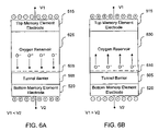
- FIG. 6A depicts a block diagram of the memory cell of FIG. 5B where oxygen accumulation near the tunnel barrier—oxygen reservoir interface results in a low conductivity region;
- FIG. 6B depicts a block diagram of the memory cell of FIG. 5B where oxygen depletion near the tunnel barrier—oxygen reservoir interface results in a low conductivity region;
- FIG. 6C depicts two block diagrams where a redox reaction between the oxygen reservoir and a complementary reservoir results in a low conductivity region
- FIG. 6D depicts a block diagram where a low conductivity region is initially fabricated, and then reduced to shrink the effective tunnel barrier width
- Nonvolatile memory requires three terminal MOSFET-based devices.
- the layout of such devices is not ideal, usually requiring an area of at least 8f 2 for each memory cell, where f is the minimum feature size.
- not all memory elements require three terminals. If, for example, a memory element is capable of changing its electrical properties (e.g., resistivity) in response to a voltage pulse, only two terminals are required. With only two terminals, a cross point array layout that allows a single cell to be fabricated to a size of 4f 2 can be utilized.
- FIG. 1A depicts a perspective view of an exemplary cross point memory array 100 employing a single layer of memory.
- a bottom layer of x-direction conductive array lines 105 is orthogonal to a top layer of y-direction conductive array lines 110 .
- the x-direction conductive array lines 105 act as a first terminal and the y-direction conductive array lines 10 act as a second terminal to a plurality of memory plugs 115 , which are located at the intersections of the conductive array lines 105 and 110 .
- the conductive array lines 105 and 10 are used to both deliver a voltage pulse to the memory plugs 115 and carry current through the memory plugs 115 in order to determine their resistive states.
- Conductive array line layers 105 and 110 can generally be constructed of any conductive material, such as aluminum, copper, tungsten or certain ceramics. Depending upon the material, a conductive array line would typically cross between 64 and 8192 perpendicular conductive array lines. Fabrication techniques, feature size and resistivity of material may allow for shorter or longer lines. Although the x-direction and y-direction conductive array lines can be of equal lengths (forming a square cross point array) they can also be of unequal lengths (forming a rectangular cross point array), which may be useful if they are made from different materials with different resistivities.
- FIG. 2A illustrates selection of a memory cell 205 in the cross point array 100 .
- the point of intersection between a single x-direction conductive array line 210 and a single y-direction conductive array line 215 uniquely identifies the single memory cell 205 .
- FIG. 2B illustrates the boundaries of the selected memory cell 205 .
- the memory cell is a repeatable unit that can be theoretically extended in one, two or even three dimensions.
- One method of repeating the memory cells in the z-direction is to use both the bottom and top surfaces of conductive array lines 105 and 110 , creating a stacked cross point array.
- FIG. 1B depicts an exemplary stacked cross point array 150 employing four memory layers 155 , 160 , 165 , and 170 .
- the memory layers are sandwiched between alternating layers of x-direction conductive array lines 175 , 180 and 185 and y-direction conductive array lines 190 and 195 such that each memory layer 155 , 160 , 165 , and 170 is associated with only one x-direction conductive array line layer and one y-direction conductive array line layer.
- top conductive array line layer 185 and bottom conductive array line layer 175 are only used to supply voltage to a single memory layer 155 and 170
- the other conductive array line layers 180 , 190 , and 195 can be used to supply voltage to both a top and a bottom memory layer 155 , 160 , 165 , or 170 .
- the repeatable cell that makes up the cross point array 100 can be considered to be a memory plug 255 , plus 1 ⁇ 2 of the space around the memory plug, plus 1 ⁇ 2 of an x-direction conductive array line 210 and 1 ⁇ 2 of a y-direction conductive array line 215 .
- 1 ⁇ 2 of a conductive array line is merely a theoretical construct, since a conductive array line would generally be fabricated to the same width, regardless of whether one or both surfaces of the conductive array line was used. Accordingly, the very top and very bottom layers of conductive array lines (which use only one surface) would typically be fabricated to the same size as all other layers of conductive array lines.
- the cross point array is not the only type of memory array that can be used with a two-terminal memory element.
- a two-dimensional transistor memory array can incorporate a two-terminal memory element. While the memory element in such an array would be a two-terminal device, the entire memory cell would be a three-terminal device.
- FIG. 3 is a generalized diagrammatic representation of a memory cell 300 that can be used in a transistor memory array.
- Each memory cell 300 includes a transistor 305 and a memory plug 310 .
- the transistor 305 is used to permit current from the data line 315 to access the memory plug 310 when an appropriate voltage is applied to the select line 320 , which is also the transistor's gate.
- the reference line 325 might span two cells if the adjacent cells are laid out as the mirror images of each other.
- FIG. 4A is a block diagram of a representative implementation of an exemplary 1 MB memory 400 A. Physical layouts might differ, but each memory bit block 405 can be formed on a separate portion of a semiconductor substrate.
- Input signals into the memory 400 A can include an address bus 430 , a control bus 440 , some power supplies 450 (typically Vcc and ground—the other signals of bus 450 can be internally generated by the 1 MB memory 400 A), and a data bus 460 .
- the control bus 440 typically includes signals to select the chip, to signal whether a read or write operation should be performed, and to enable the output buffers when the chip is in read mode.
- the address bus 430 specifies which location in the memory array is accessed—some addresses going to the X block 470 (typically including a predecoder and an X-decoder) to select one line out of the horizontal array lines.
- the other addresses go to a Y block 480 (typically including a predecoder and a Y-decoder) to apply the appropriate voltage on specific vertical lines.
- Each memory bit block 405 operates on one line of the memory chip data bus 460 .
- FIG. 4B is a block diagram of an exemplary memory 400 B that includes sensing circuits 415 that are capable of reading multiple bits.
- the simultaneous reading of multiple bits involves sensing current from multiple y-lines simultaneously.
- each y-line can either have an associated driver circuit or a group of y-lines can share a single driver circuit if the non-selected lines in the group are held to a constant voltage that would not cause the unselected memory plugs to experience any change in resistance.
- the page register may include 8 latches, in which case the y-block would decode 1 out of 128 y-lines and connect the selected lines to block 495 .
- the driver circuit then writes the 1 or 0 to the appropriate memory plug.
- the writing can be performed in multiple cycles.
- all the 1s can be written during a first cycle and all the 0s can be written during a second cycle.
- certain memory plugs can have multiple stable distinct resistive states.
- driver circuits could program, for example, states of 00, 01, 10 or 11 by varying write voltage magnitude or pulse length. Regardless of how the write operations and the read operations are implemented, they can collectively be described as the normal operations of the memory array 420 and are, of course, dictated by the specific chip architecture that is used.
- such an architecture can be expanded to create a memory where one array handles all the bits of the data bus, as opposed to having multiple arrays, or memory bit blocks as described above.
- the data bus, or memory data organization, also called data width is 16-bit wide
- the y-block of one cross point array can be made to decode 16 lines simultaneously.
- Each memory plug contains layers of materials that may be desirable for fabrication or functionality. For example, a non-ohmic characteristic that exhibit a very high resistance regime for a certain range of voltages (V NO ⁇ to V NO+ ) and a very low resistance regime for voltages above and below that range might be desirable. In a cross point array, a non-ohmic characteristic could prevent leakage during reads and writes if half of both voltages were within the range of voltages V NO ⁇ to V NO+ . If each conductive array line carried 1 ⁇ 2 V W , the current path would be the memory plug at the intersection of the two conductive array lines that each carried 1 ⁇ 2 V W . The other memory plugs would exhibit such high resistances from the non-ohmic characteristic that current would not flow through the half-selected plugs.
- a non-ohmic device might be used to cause the memory plug to exhibit a non-linear resistive characteristic.
- Exemplary non-ohmic devices include three-film metal-insulator-metal (MIM) structures and back-to-back diodes in series. Separate non-ohmic devices, however, may not be necessary.
- MIM metal-insulator-metal
- Certain fabrications of the memory plug can cause a non-ohmic characteristic to be imparted to the memory cell. While a non-ohmic characteristic might be desirable in certain arrays, it may not be required in other arrays.
- Electrodes will typically be desirable components of the memory plugs, a pair of electrodes sandwiching the memory element. If the only purpose of the electrodes is as a barrier to prevent metal inter-diffusion, then a thin layer of non-reactive metal, e.g. TiN, TaN, Pt, Au, and certain metal oxides could be used. However, electrodes may provide advantages beyond simply acting as a metal inter-diffusion barrier. Electrodes (formed either with a single layer or multiple layers) can perform various functions, including: prevent the diffusion of metals, oxygen, hydrogen and water; act as a seed layer in order to form a good lattice match with other layers; act as adhesion layers; reduce stress caused by uneven coefficients of thermal expansion; and provide other benefits. Additionally, the choice of electrode layers can affect the memory effect properties of the memory plug and become part of the memory element.
- memory element electrodes are the electrodes (or, in certain circumstances, the portion of the conductive array lines) that the memory elements are sandwiched in-between. As used herein, memory element electrodes are what allow other components to be electrically connected to the memory element. It should be noted that both cross point arrays and transistor memory arrays have exactly two memory element electrodes since the memory plug has exactly two terminals, regardless of how many terminals the memory cell has. Those skilled in the art will appreciate that a floating gate transistor, if used as a memory element, would have exactly three memory element electrodes (source, drain and gate).
- the memory effect is a hysteresis that exhibits a resistive state change upon application of a voltage while allowing non-destructive reads.
- a non-destructive read means that the read operation has no effect on the resistive state of the memory element.
- Measuring the resistance of a memory cell is generally accomplished by detecting either current after the memory cell is held to a known voltage, or voltage after a known current flows through the memory cell. Therefore, a memory cell that is placed in a high resistive state R 0 upon application of ⁇ V W and a low resistive state R 1 upon application of +V W should be unaffected by a read operation performed at ⁇ V R or +V R . In such materials a write operation is not necessary after a read operation. It should be appreciated that the magnitude of
- programming R 1 would be accomplished with a voltage pulse of V P
- programming R 0 would be accomplished with a voltage pulse greater than V P
- reads would occur with a voltages below V T .
- Intermediate resistive states for multi-level memory cells
- the R 1 state of the memory plug may have a best value of 10 k ⁇ to 100 k ⁇ . If the R 1 state resistance is much less than 10 k ⁇ , the current consumption will be increased because the cell current is high, and the parasitic resistances will have a larger effect. If the R 1 state value is much above 100 k ⁇ , the RC delays will increase access time. However, workable single state resistive values may also be achieved with resistances as low as 5 k ⁇ and as high as 1 M ⁇ . Typically, a single state memory would have the operational resistances of R 0 and R 1 separated by a factor of 10.
- multi-bit resistive memory cells are possible. Changes in the resistive property of the memory plugs that are greater than a factor of 10 might be desirable in multi-bit resistive memory cells.
- the memory plug might have a high resistive state of R 00 , a medium-high resistive state of R 01 , a medium-low resistive state of R 10 and a low resistive state of R 11 . Since multi-bit memories typically have access times longer than single-bit memories, using a factor greater than a 10 times change in resistance from R 11 to R 00 is one way to make a multi-bit memory as fast as a single-bit memory.
- a memory cell that is capable of storing two bits might have the low resistive state be separated from the high resistive state by a factor of 100.
- a memory cell that is capable of storing three or four bits of information might require the low resistive state be separated from the high resistive state by a factor of 1000.
- Tunneling is a process whereby electrons pass through a barrier in the presence of an electric field. Tunneling Is exponentially dependant on a barrier's width and the square root of its height. Barrier height is typically defined as the potential difference between the Fermi energy of a first conducting material and the band edge of a second insulating material. The Fermi energy is that energy at which the probability of occupation of an electron suite is 50%. Barrier width is the physical thickness of the insulating material.
- the barrier height might be modified if carriers or ions are introduced into the second insulating material, creating an additional electric field.
- a barrier's width can be changed if the barrier physically changes shape, either growing or shrinking. In the presence of a high electric field, both mechanisms could result in a change in conductivity.
- barrier height modification includes (but not limited to) barrier height modification, carrier charge trapping space-charge limited currents, thermionic emission limited conduction, and/or electrothermal Poole-Frenkel emission.
- FIG. 5A is a block diagram representing the basic components of a memory element 500
- FIG. 5B is a block diagram of the memory element 500 in a two-terminal memory cell
- FIG. 5C is a block diagram of the memory element in a three-terminal memory cell.
- FIG. 5A shows a tunnel barrier 505 and an ion reservoir 510 , two basic components of the memory element 500 .
- FIG. 5B shows the memory element 500 between a top memory electrode 515 and a bottom memory electrode 520 .
- the orientation of the memory element i.e., whether the tunnel barrier 505 is near the top memory electrode 515 or the bottom memory electrode 520 ) may be important for processing considerations, including the necessity of seed layers and how the tunnel barrier reacts with the ion reservoir 510 during deposition.
- FIG. 5C shows the memory element 500 oriented with the tunnel barrier 505 on the bottom in a three-terminal transistor device, having a source memory element electrode 525 , gate memory element electrode 530 and a drain memory element electrode 535 . In such an orientation, the tunnel barrier 505 could also function as a gate oxide.
- the tunnel barrier 505 will typically be less than 50 angstroms. If the tunnel barrier 505 is much greater than 50 angstroms, then the electric field that is required to move electrons through the memory element 500 via tunneling becomes too high for most electronic devices. Depending on the tunnel barrier 505 material, a preferred tunnel barrier 505 width might be between 15 and 20 angstroms for circuits where rapid access times (on the order of tens of nanoseconds, typically below 100 ns) in small dimension devices (on the order of hundreds of nanometers) are desired.
- the tunnel barrier 505 is an insulator. While some embodiments have other requirements of the tunnel barrier 505 (e.g., being permeable to positive or negative ions, as described in connection with FIG. 6C ), the main conduction mechanism through the tunnel barrier 505 should be tunneling. Insulators suitable for some embodiments include various metal oxides such as Al 2 O 3 , Ta 2 O 5 and HfO 2 .
- the tunnel barrier 505 will typically be of very high quality, being as uniform as possible to allow for predictability in the voltage required to obtain a current through the memory element 500 . Atomic layer deposition and plasma oxidation are examples of methods that can be used to create very high quality tunnel barriers.
- tunnel barriers can be obtained by allowing a reactive metal to simply come in contact with an ion reservoir 510 , as described in PCT International Application No. PCT/US2004/013836, filed May 3, 2004, already incorporated herein by reference, such barriers may be of low quality and lacking uniformity.
- the electric field at the tunnel barrier 505 is typically high enough to promote tunneling at thicknesses less than 50 angstroms.
- the electric field is typically higher than the electric field at other points in the circuit due to factors such as the relatively high serial resistance of the tunnel barrier 505 compared to the rest of the circuit and the accumulation of charge at the interface.
- the electric field not only enables tunneling, but, with the appropriate ion reservoir 510 , also allows the effective width of the tunnel barrier 505 to change.
- the ion reservoir 510 is a material that is conductive enough to allow current to flow and has mobile ions.
- the ion reservoir 510 can be, for example, an oxygen reservoir with mobile oxygen ions. Oxygen ions are negative in charge, and will flow in the direction opposite of current. As will be described in FIG. 6A , FIG. 6 B, FIG. 6C , and FIG. 6D the movement of oxygen ions can potentially modify the effective barrier width in various ways.
- FIG. 6A is a block diagram where oxygen accumulation near the tunnel barrier 505 —oxygen reservoir 625 interface results in a low conductivity region 605 .
- This low conductivity region 605 is cumulative with the tunnel barrier 505 , forcing electrons to tunnel a greater distance to reach the second memory element electrode 520 .
- the low conductivity region 605 can be just a few angstroms wide and still have a very noticeable effect on the memory element's effective resistance.
- a low conductivity region 605 to be created in the oxygen reservoir 625 it must have the physical property of being less conductive in an oxygen-rich state.
- An example of a conductive material that has mobile oxygen ions and is less conductive in an oxygen-rich state is reduced strontium titanate (STO) and similar perovskites (a perovskite generally being in the form of an ABX 3 structure, where A has an atomic size of 1.0-1.4 ⁇ and B has an atomic size of 0.45-0.75 ⁇ for the case where X is either oxygen or fluorine).
- STO strontium titanate
- perovskites a perovskite generally being in the form of an ABX 3 structure, where A has an atomic size of 1.0-1.4 ⁇ and B has an atomic size of 0.45-0.75 ⁇ for the case where X is either oxygen or fluorine.
- the oxygen-rich state should be stable enough to resist the migratory force that results from a concentration gradient.
- oxygen reservoir 625 it may be important to either avoid or maintain an oxygen-deficient state in the bulk of the oxygen reservoir 625 to maintain conductivity.
- a larger oxygen reservoir 625 will allow for the oxygen-deficient effects to be distributed throughout the material.
- the oxygen reservoir 625 is a perovskite it might be important that the ABO 3 structure have a slight oxygen deficiency in order to maintain conductivity. If two atomic layers of stoichiometric ABO 3 were sufficient to produce an appropriate low conductivity region 605 , then 400 atomic layers of ABO 3-x would (assuming a constant deficiency gradient) vary the oxygen deficiency of the ABO 3-x oxygen reservoir 625 by 0.5%.
- both states of the oxygen reservoir 625 should be conductive.
- oxygen were available from other sources (e.g., if the first memory element electrode 515 were exposed to the atmosphere and permeable to oxygen) the height of the oxygen reservoir 625 may not be as critical.
- a voltage of opposite polarity should be sufficient to push the excess oxygen out of the low conductivity region 605 and back into the oxygen deficient regions of the oxygen reservoir 625 .
- the activation energy of reducing the low conductivity region 605 in a redox reaction is greater than or less than the energy required to create the low conductivity region can inform the read polarity choice. If reducing the low conductivity region 605 with a positive voltage takes more energy than creating an oxygen-rich conductivity region 605 with a negative voltage, then positive reads have a lesser chance of disturbing the resistive state of the memory element.
- FIG. 6B is a block diagram where oxygen depletion near the tunnel barrier 505 —oxygen reservoir 630 interface results in a low conductivity region 610 .
- a low conductivity region 610 to be created in the oxygen reservoir 630 it must have the physical property of being less conductive in an oxygen-deficient state.
- Some examples of materials that have mobile oxygen ions and are less conductive in an oxygen-deficient state are Pr 0.7 Ca 0.3 MnO 3 , Pr 0.5 Ca 0.5 MnO 3 and other PCMO perovskites.
- FIG. 6C shows two block diagrams where a redox reaction between the oxygen reservoir 635 and a complementary reservoir 615 results in a low conductivity region 620 .
- the ion reservoir 510 (see FIG. 5A ) is made up of negative oxygen ions
- an appropriate complementary reservoir 615 would include mobile positively charged metal ions (designated as M + in FIG. 6C ).
- M + mobile positively charged metal ions
- the mechanism is similar to the embodiment of FIG. 6A , except positively charged metal ions M + migrate through the tunnel barrier 505 to combine with oxygen ions O ⁇ in the oxygen reservoir 635 , creating the low conductivity region 620 .
- redox reaction can occur at either the top or bottom surface of the tunnel barrier 505 .
- the low conductivity region 620 will form at the top of the tunnel barrier 505 if the mobility of the complementary ions M + is greater than the mobility of the oxygen ions through the tunnel barrier 505 . Conversely, it the mobility of oxygen ions O ⁇ is greater than the mobility of the complementary ions M + through the tunnel barrier 505 , then the low conductivity region 620 will form at the bottom of the tunnel barrier 505 as shown in the second diagram on the right side of the drawing sheet of FIG. 6C . In the first diagram the free oxygen ions (designated as O ⁇ in FIG. 6C ) in the oxygen reservoir 635 do not move into the tunnel barrier 505 .
- the free metal ions M + the metal reservoir 615 do not move into the tunnel barrier 505 .
- the metal reservoir 615 is any material that is conductive enough to allow current to flow and has free metal ions M + .
- the metal reservoir 615 may be the non-oxidized form (either the bare metal(s) or the reduced non-stoichiometric oxide) of the same material that is used for the tunnel barrier 505 .
- the effective width of the barrier is limited only by the effect of ion deficiency in the ion reservoir and the availability of ions in the complimentary reservoir, many different barrier widths can be formed if large enough reservoirs are used. Accordingly, multiple bits per cell can be easily implemented with different resistive states.
- the term “memory element” includes all the layers that contribute to the memory effect. Accordingly, in the embodiment of FIG. 6C , the memory element includes the oxygen reservoir 635 , the low conductivity region 620 (when the memory cell is in the high resistive state), the tunnel barrier 505 , and the metal reservoir 615 . When the memory element is in the low resistive state, the tunnel barrier 505 has the lowest conductivity (i.e., the highest series resistance) relative to all the other layers of the memory element, including the oxygen reservoir 635 and the entire metal reservoir 615 as neither of these would have a low conductivity region 620 in the low resistive state.
- FIG. 6D is a block diagram where a low conductivity region 645 is initially fabricated, and then reduced to shrink the effective tunnel barrier width. Since the memory element is initially fabricated with the low conductivity region 645 , an appropriate voltage would reduce the material into more conductive components. This embodiment will typically be used only in reprogrammable memory cells because the activation energy to re-oxide the material is typically not very high.
- the problem of an oxygen-deficient oxygen reservoir 640 is then diminished since the oxygen reservoir 640 does not need to supply any oxygen ions to the low conductivity region 645 .
- the oxygen reservoir 640 will need to be able to maintain its conductivity once the excess oxygen ions are removed from the low conductivity region 645 and dispersed into the oxygen reservoir 640 .
- the tunnel barrier 505 and the low conductivity region 645 could be a single material for ease of fabrication.
Abstract
Description
Claims (30)
Priority Applications (24)
| Application Number | Priority Date | Filing Date | Title |
|---|---|---|---|
| US10/934,951 US7538338B2 (en) | 2004-09-03 | 2004-09-03 | Memory using variable tunnel barrier widths |
| US11/095,026 US20060171200A1 (en) | 2004-02-06 | 2005-03-30 | Memory using mixed valence conductive oxides |
| JP2007530487A JP2008512857A (en) | 2004-09-03 | 2005-09-01 | Memory using mixed valence conductive oxide |
| CN200580038024.5A CN101057298B (en) | 2004-09-03 | 2005-09-01 | Memory and method for forming memory effect |
| EP05794930A EP1800314A2 (en) | 2004-09-03 | 2005-09-01 | Memory using mixed valence conductive oxides |
| CN2012101934211A CN102694122A (en) | 2004-09-03 | 2005-09-01 | Two terminal re-writeable non-volatile ion transport memory device |
| EP10182254A EP2284840A3 (en) | 2004-09-03 | 2005-09-01 | Memory using mixed valence conductive oxides |
| PCT/US2005/031913 WO2006029228A2 (en) | 2004-09-03 | 2005-09-01 | Memory using mixed valence conductive oxides |
| KR1020077005463A KR20070047341A (en) | 2004-09-03 | 2005-09-01 | Memory using mixed valence conductive oxides |
| US12/004,292 US8020132B2 (en) | 2004-02-06 | 2007-12-19 | Combined memories in integrated circuits |
| US12/454,698 US7985963B2 (en) | 2004-09-03 | 2009-05-21 | Memory using variable tunnel barrier widths |
| US12/456,627 US20090303772A1 (en) | 2004-02-06 | 2009-06-18 | Two-Terminal Reversibly Switchable Memory Device |
| US12/456,677 US20090303773A1 (en) | 2004-02-06 | 2009-06-18 | Multi-terminal reversibly switchable memory device |
| US13/191,245 US20110278532A1 (en) | 2004-09-03 | 2011-07-26 | Tri layer metal oxide rewritable non volatile two terminal memory element |
| US13/224,173 US8141021B2 (en) | 2004-02-06 | 2011-09-01 | Combined memories in integrated circuits |
| US13/329,063 US20120087174A1 (en) | 2004-09-03 | 2011-12-16 | Two Terminal Re Writeable Non Volatile Ion Transport Memory Device |
| US13/425,256 US8347254B2 (en) | 2004-02-06 | 2012-03-20 | Combined memories in integrated circuits |
| JP2012175072A JP2012238893A (en) | 2004-09-03 | 2012-08-07 | Memory using mixed valence conductive oxides |
| US14/463,518 US9159913B2 (en) | 2004-02-06 | 2014-08-19 | Two-terminal reversibly switchable memory device |
| US14/844,805 US9831425B2 (en) | 2004-02-06 | 2015-09-03 | Two-terminal reversibly switchable memory device |
| US15/797,452 US10224480B2 (en) | 2004-02-06 | 2017-10-30 | Two-terminal reversibly switchable memory device |
| US16/262,841 US10680171B2 (en) | 2004-02-06 | 2019-01-30 | Two-terminal reversibly switchable memory device |
| US16/864,051 US11063214B2 (en) | 2004-02-06 | 2020-04-30 | Two-terminal reversibly switchable memory device |
| US17/194,609 US11672189B2 (en) | 2004-02-06 | 2021-03-08 | Two-terminal reversibly switchable memory device |
Applications Claiming Priority (1)
| Application Number | Priority Date | Filing Date | Title |
|---|---|---|---|
| US10/934,951 US7538338B2 (en) | 2004-09-03 | 2004-09-03 | Memory using variable tunnel barrier widths |
Related Parent Applications (1)
| Application Number | Title | Priority Date | Filing Date |
|---|---|---|---|
| US10/773,549 Continuation-In-Part US7082052B2 (en) | 2004-02-06 | 2004-02-06 | Multi-resistive state element with reactive metal |
Related Child Applications (2)
| Application Number | Title | Priority Date | Filing Date |
|---|---|---|---|
| US11/095,026 Continuation-In-Part US20060171200A1 (en) | 2004-02-06 | 2005-03-30 | Memory using mixed valence conductive oxides |
| US12/454,698 Continuation US7985963B2 (en) | 2004-09-03 | 2009-05-21 | Memory using variable tunnel barrier widths |
Publications (2)
| Publication Number | Publication Date |
|---|---|
| US20060050598A1 US20060050598A1 (en) | 2006-03-09 |
| US7538338B2 true US7538338B2 (en) | 2009-05-26 |
Family
ID=35996059
Family Applications (3)
| Application Number | Title | Priority Date | Filing Date |
|---|---|---|---|
| US10/934,951 Active 2025-09-17 US7538338B2 (en) | 2004-02-06 | 2004-09-03 | Memory using variable tunnel barrier widths |
| US12/454,698 Expired - Fee Related US7985963B2 (en) | 2004-09-03 | 2009-05-21 | Memory using variable tunnel barrier widths |
| US13/191,245 Abandoned US20110278532A1 (en) | 2004-09-03 | 2011-07-26 | Tri layer metal oxide rewritable non volatile two terminal memory element |
Family Applications After (2)
| Application Number | Title | Priority Date | Filing Date |
|---|---|---|---|
| US12/454,698 Expired - Fee Related US7985963B2 (en) | 2004-09-03 | 2009-05-21 | Memory using variable tunnel barrier widths |
| US13/191,245 Abandoned US20110278532A1 (en) | 2004-09-03 | 2011-07-26 | Tri layer metal oxide rewritable non volatile two terminal memory element |
Country Status (2)
| Country | Link |
|---|---|
| US (3) | US7538338B2 (en) |
| CN (1) | CN101057298B (en) |
Cited By (52)
| Publication number | Priority date | Publication date | Assignee | Title |
|---|---|---|---|---|
| US20070290186A1 (en) * | 2006-05-04 | 2007-12-20 | El Mostafa Bourim | Non-volatile variable resistance memory device and method of fabricating the same |
| US20080048164A1 (en) * | 2006-07-11 | 2008-02-28 | Matsushita Electric Industrial Co., Ltd. | Electro-resistance element, method of manufacturing the same and electro-resistance memory using the same |
| US20080090337A1 (en) * | 2006-10-03 | 2008-04-17 | Williams R Stanley | Electrically actuated switch |
| US20080109775A1 (en) * | 2004-02-06 | 2008-05-08 | Unity Semiconductor Corporation | Combined memories in integrated circuits |
| US20080116438A1 (en) * | 2006-11-16 | 2008-05-22 | Samsung Electronics Co., Ltd. | Resistive random access memory having a solid solution layer and method of manufacturing the same |
| US20080296550A1 (en) * | 2007-05-30 | 2008-12-04 | Samsung Electronics Co., Ltd. | Resistive random access memory device and methods of manufacturing and operating the same |
| US20090027977A1 (en) * | 2007-07-26 | 2009-01-29 | Unity Semiconductor Corporation | Low read current architecture for memory |
| US20090231906A1 (en) * | 2004-09-03 | 2009-09-17 | Unity Semiconductor Corporation | Memory using variable tunnel barrier widths |
| US20090237995A1 (en) * | 2006-10-05 | 2009-09-24 | Unity Semiconductor Corporation | Scaleable memory Systems Using Third Dimension Memory |
| US20100117053A1 (en) * | 2008-11-12 | 2010-05-13 | Sekar Deepak C | Metal oxide materials and electrodes for re-ram |
| US20100159688A1 (en) * | 2008-12-19 | 2010-06-24 | Unity Semiconductor Corporation | Device fabrication |
| US20110038198A1 (en) * | 2006-11-03 | 2011-02-17 | New York University | Electronic devices based on current induced magnetization dynamics in single magnetic layers |
| US20110155990A1 (en) * | 2007-07-26 | 2011-06-30 | Unity Semiconductor Corporation | Continuous plane of thin-film materials for a two-terminal cross-point memory |
| US20110188283A1 (en) * | 2010-02-01 | 2011-08-04 | Unity Semiconductor Corporation | Circuits and techniques to compensate data signals for variations of parameters affecting memory cells in cross-point arrays |
| US20110188281A1 (en) * | 2010-01-29 | 2011-08-04 | Unity Semiconductor Corporation | Local bit lines and methods of selecting the same to access memory elements in cross-point arrays |
| US20110188282A1 (en) * | 2010-02-02 | 2011-08-04 | Unity Semiconductor Corporation | Memory architectures and techniques to enhance throughput for cross-point arrays |
| US20110227030A1 (en) * | 2009-01-13 | 2011-09-22 | Pickett Matthew D | Memristor Having a Triangular Shaped Electrode |
| US20110291066A1 (en) * | 2010-06-01 | 2011-12-01 | In-Gyu Baek | Nonvolatile Memory Devices Having Cells with Oxygen Diffusion Barrier Layers Therein and Methods of Manufacturing the Same |
| US20120001143A1 (en) * | 2009-03-27 | 2012-01-05 | Dmitri Borisovich Strukov | Switchable Junction with Intrinsic Diode |
| US20120063239A1 (en) * | 2007-08-16 | 2012-03-15 | Unity Semiconductor Corporation | Circuitry And Method For Indicating A Memory |
| US20120106232A1 (en) * | 2010-11-01 | 2012-05-03 | Meade Roy E | Memory Cells, Methods of Programming Memory Cells, and Methods of Forming Memory Cells |
| US20120267598A1 (en) * | 2009-10-09 | 2012-10-25 | Nec Corporation | Semiconductor device and method for manufacturing the same |
| US20130003437A1 (en) * | 2011-06-28 | 2013-01-03 | Unity Semiconductor Corporation | Multilayer Cross-Point Memory Array Having Reduced Disturb Susceptibility |
| US8652909B2 (en) | 2010-12-27 | 2014-02-18 | Micron Technology, Inc. | Methods of forming a nonvolatile memory cell and methods of forming an array of nonvolatile memory cells array of nonvolatile memory cells |
| US8674336B2 (en) | 2008-04-08 | 2014-03-18 | Micron Technology, Inc. | Non-volatile resistive oxide memory cells, non-volatile resistive oxide memory arrays, and methods of forming non-volatile resistive oxide memory cells and memory arrays |
| US8681531B2 (en) | 2011-02-24 | 2014-03-25 | Micron Technology, Inc. | Memory cells, methods of forming memory cells, and methods of programming memory cells |
| US8686389B1 (en) | 2012-10-16 | 2014-04-01 | Intermolecular, Inc. | Diffusion barrier layer for resistive random access memory cells |
| US8737151B2 (en) | 2007-07-26 | 2014-05-27 | Unity Semiconductor Corporation | Low read current architecture for memory |
| US8743589B2 (en) | 2010-04-22 | 2014-06-03 | Micron Technology, Inc. | Arrays of vertically stacked tiers of non-volatile cross point memory cells and methods of reading a data value stored by an array of vertically stacked tiers of non-volatile cross point memory cells |
| US8753949B2 (en) | 2010-11-01 | 2014-06-17 | Micron Technology, Inc. | Nonvolatile memory cells and methods of forming nonvolatile memory cells |
| US8759809B2 (en) | 2010-10-21 | 2014-06-24 | Micron Technology, Inc. | Integrated circuitry comprising nonvolatile memory cells having platelike electrode and ion conductive material layer |
| US8760910B2 (en) | 2010-04-22 | 2014-06-24 | Micron Technology, Inc. | Arrays of vertically stacked tiers of non-volatile cross point memory cells, methods of forming arrays of vertically stacked tiers of non-volatile cross point memory cells, and methods of reading a data value stored by an array of vertically stacked tiers of non-volatile cross point memory cells |
| US8854863B2 (en) | 2011-04-15 | 2014-10-07 | Micron Technology, Inc. | Arrays of nonvolatile memory cells and methods of forming arrays of nonvolatile memory cells |
| US8878152B2 (en) | 2012-02-29 | 2014-11-04 | Intermolecular, Inc. | Nonvolatile resistive memory element with an integrated oxygen isolation structure |
| US8976566B2 (en) | 2010-09-29 | 2015-03-10 | Micron Technology, Inc. | Electronic devices, memory devices and memory arrays |
| US9093368B2 (en) | 2011-01-20 | 2015-07-28 | Micron Technology, Inc. | Nonvolatile memory cells and arrays of nonvolatile memory cells |
| US9111788B2 (en) | 2008-06-18 | 2015-08-18 | Micron Technology, Inc. | Memory device constructions, memory cell forming methods, and semiconductor construction forming methods |
| US9178142B2 (en) | 2013-03-04 | 2015-11-03 | Intermolecular, Inc. | Doped electrodes used to inhibit oxygen loss in ReRAM device |
| US9343145B2 (en) | 2008-01-15 | 2016-05-17 | Micron Technology, Inc. | Memory cells, memory cell programming methods, memory cell reading methods, memory cell operating methods, and memory devices |
| US9343665B2 (en) | 2008-07-02 | 2016-05-17 | Micron Technology, Inc. | Methods of forming a non-volatile resistive oxide memory cell and methods of forming a non-volatile resistive oxide memory array |
| US9373410B1 (en) | 2014-07-25 | 2016-06-21 | Crossbar, Inc. | MLC OTP operation in A-Si RRAM |
| US9412421B2 (en) | 2010-06-07 | 2016-08-09 | Micron Technology, Inc. | Memory arrays |
| US20160268418A1 (en) * | 2013-07-29 | 2016-09-15 | Samsung Electronics Co., Ltd. | Nonvolatile memory transistor and device including the same |
| US9454997B2 (en) | 2010-12-02 | 2016-09-27 | Micron Technology, Inc. | Array of nonvolatile memory cells having at least five memory cells per unit cell, having a plurality of the unit cells which individually comprise three elevational regions of programmable material, and/or having a continuous volume having a combination of a plurality of vertically oriented memory cells and a plurality of horizontally oriented memory cells; array of vertically stacked tiers of nonvolatile memory cells |
| US9484533B2 (en) | 2005-03-30 | 2016-11-01 | Unity Semiconductor Corporation | Multi-layered conductive metal oxide structures and methods for facilitating enhanced performance characteristics of two-terminal memory cells |
| US9502102B1 (en) * | 2014-07-25 | 2016-11-22 | Crossbar, Inc. | MLC OTP operation with diode behavior in ZnO RRAM devices for 3D memory |
| CN106299111A (en) * | 2015-06-23 | 2017-01-04 | 北京有色金属研究总院 | One is exempted to electrically activate complementary resistance-variable storing device and preparation method thereof |
| US9577186B2 (en) | 2008-05-02 | 2017-02-21 | Micron Technology, Inc. | Non-volatile resistive oxide memory cells and methods of forming non-volatile resistive oxide memory cells |
| US20170133391A1 (en) * | 2014-06-20 | 2017-05-11 | Floadia Corporation | Non-Volatile Semiconductor Memory Device |
| US9842882B1 (en) * | 2016-05-18 | 2017-12-12 | SK Hynix Inc. | Electronic device |
| US10340312B2 (en) | 2004-02-06 | 2019-07-02 | Hefei Reliance Memory Limited | Memory element with a reactive metal layer |
| US10586765B2 (en) | 2017-06-22 | 2020-03-10 | Tokyo Electron Limited | Buried power rails |
Families Citing this family (50)
| Publication number | Priority date | Publication date | Assignee | Title |
|---|---|---|---|---|
| US8003511B2 (en) * | 2008-12-19 | 2011-08-23 | Unity Semiconductor Corporation | Memory cell formation using ion implant isolated conductive metal oxide |
| US7522468B2 (en) * | 2006-06-08 | 2009-04-21 | Unity Semiconductor Corporation | Serial memory interface |
| US7747817B2 (en) * | 2006-06-28 | 2010-06-29 | Unity Semiconductor Corporation | Performing data operations using non-volatile third dimension memory |
| US7619945B2 (en) | 2006-08-18 | 2009-11-17 | Unity Semiconductor Corporation | Memory power management |
| US8058643B2 (en) | 2006-09-29 | 2011-11-15 | The Board Of Trustees Of The Leland Stanford Junior University | Electrochemical memory with internal boundary |
| US7724562B2 (en) * | 2006-11-02 | 2010-05-25 | The Board Of Trustees Of The Leland Stanford Junior University | Electrochemical memory with heater |
| US7765380B2 (en) * | 2007-01-19 | 2010-07-27 | Unity Semiconductor Corporation | Fast data access through page manipulation |
| US7678607B2 (en) | 2007-02-05 | 2010-03-16 | Intermolecular, Inc. | Methods for forming resistive switching memory elements |
| US7704789B2 (en) * | 2007-02-05 | 2010-04-27 | Intermolecular, Inc. | Methods for forming resistive switching memory elements |
| US7972897B2 (en) * | 2007-02-05 | 2011-07-05 | Intermolecular, Inc. | Methods for forming resistive switching memory elements |
| US8097878B2 (en) * | 2007-03-05 | 2012-01-17 | Intermolecular, Inc. | Nonvolatile memory elements with metal-deficient resistive-switching metal oxides |
| US7629198B2 (en) * | 2007-03-05 | 2009-12-08 | Intermolecular, Inc. | Methods for forming nonvolatile memory elements with resistive-switching metal oxides |
| WO2008140979A1 (en) * | 2007-05-09 | 2008-11-20 | Intermolecular, Inc. | Resistive-switching nonvolatile memory elements |
| US8294219B2 (en) * | 2007-07-25 | 2012-10-23 | Intermolecular, Inc. | Nonvolatile memory element including resistive switching metal oxide layers |
| WO2009015297A1 (en) | 2007-07-25 | 2009-01-29 | Intermolecular, Inc. | Multistate nonvolatile memory elements |
| US7995371B2 (en) * | 2007-07-26 | 2011-08-09 | Unity Semiconductor Corporation | Threshold device for a memory array |
| US7813210B2 (en) * | 2007-08-16 | 2010-10-12 | Unity Semiconductor Corporation | Multiple-type memory |
| WO2009025037A1 (en) * | 2007-08-22 | 2009-02-26 | Fujitsu Limited | Resistance variable element |
| US7996600B2 (en) | 2007-08-30 | 2011-08-09 | Unity Semiconductor Corporation | Memory emulation in an electronic organizer |
| US8164656B2 (en) * | 2007-08-31 | 2012-04-24 | Unity Semiconductor Corporation | Memory emulation in an image capture device |
| US7746710B2 (en) * | 2008-01-10 | 2010-06-29 | Micron Technology, Inc. | Data bus power-reduced semiconductor storage apparatus |
| DE102008024078A1 (en) | 2008-05-17 | 2009-12-17 | Forschungszentrum Jülich GmbH | Memory and method for writing and reading information in a memory |
| JP4469023B2 (en) * | 2008-07-11 | 2010-05-26 | パナソニック株式会社 | Nonvolatile memory element, manufacturing method thereof, and nonvolatile semiconductor device using the nonvolatile memory element |
| JP2010044827A (en) * | 2008-08-13 | 2010-02-25 | Toshiba Corp | Nonvolatile semiconductor storage device |
| US8264864B2 (en) * | 2008-12-19 | 2012-09-11 | Unity Semiconductor Corporation | Memory device with band gap control |
| US8390100B2 (en) * | 2008-12-19 | 2013-03-05 | Unity Semiconductor Corporation | Conductive oxide electrodes |
| US8421048B2 (en) * | 2009-07-13 | 2013-04-16 | Seagate Technology Llc | Non-volatile memory with active ionic interface region |
| WO2011007538A1 (en) * | 2009-07-13 | 2011-01-20 | パナソニック株式会社 | Variably resistant element and variably resistant memory device |
| US8045364B2 (en) * | 2009-12-18 | 2011-10-25 | Unity Semiconductor Corporation | Non-volatile memory device ion barrier |
| US8796656B2 (en) | 2010-06-04 | 2014-08-05 | Micron Technology, Inc. | Oxide based memory |
| US20120012897A1 (en) * | 2010-07-16 | 2012-01-19 | Unity Semiconductor Corporation | Vertically Fabricated BEOL Non-Volatile Two-Terminal Cross-Trench Memory Array with Two-Terminal Memory Elements and Method of Fabricating the Same |
| JP5566252B2 (en) * | 2010-10-13 | 2014-08-06 | ラピスセミコンダクタ株式会社 | Semiconductor memory |
| US8611141B2 (en) | 2011-09-21 | 2013-12-17 | Crocus Technology Inc. | Magnetic random access memory devices including heating straps |
| US8611140B2 (en) * | 2011-09-21 | 2013-12-17 | Crocus Technology Inc. | Magnetic random access memory devices including shared heating straps |
| US9299926B2 (en) | 2012-02-17 | 2016-03-29 | Intermolecular, Inc. | Nonvolatile memory device using a tunnel oxide layer and oxygen blocking layer as a current limiter element |
| JP2013187336A (en) * | 2012-03-07 | 2013-09-19 | Toshiba Corp | Nonvolatile semiconductor memory device |
| KR101929941B1 (en) * | 2012-08-10 | 2018-12-18 | 삼성전자 주식회사 | Resistance switching material element and device applying the same |
| US8633084B1 (en) | 2012-10-17 | 2014-01-21 | Micron Technology, Inc. | Methods of forming a memory cell having programmable material that comprises a multivalent metal oxide portion and an oxygen containing dielectric portion |
| US9159406B2 (en) * | 2012-11-02 | 2015-10-13 | Sandisk Technologies Inc. | Single-level cell endurance improvement with pre-defined blocks |
| US9515262B2 (en) | 2013-05-29 | 2016-12-06 | Shih-Yuan Wang | Resistive random-access memory with implanted and radiated channels |
| WO2014194069A2 (en) | 2013-05-29 | 2014-12-04 | Shih-Yuan Wang | Resistive random-access memory formed without forming voltage |
| US8981334B1 (en) * | 2013-11-01 | 2015-03-17 | Micron Technology, Inc. | Memory cells having regions containing one or both of carbon and boron |
| US20150249113A1 (en) * | 2014-02-28 | 2015-09-03 | Kabushiki Kaisha Toshiba | Nonvolatile memory device |
| TWI553925B (en) | 2014-09-26 | 2016-10-11 | 華邦電子股份有限公司 | Self-rectifying resistive random access memory cell structure |
| JP6430306B2 (en) | 2015-03-19 | 2018-11-28 | 東芝メモリ株式会社 | Nonvolatile memory device |
| US20170117464A1 (en) * | 2015-10-22 | 2017-04-27 | Winbond Electronics Corp. | Resistive random access memory device |
| US9553263B1 (en) | 2015-11-06 | 2017-01-24 | Micron Technology, Inc. | Resistive memory elements including buffer materials, and related memory cells, memory devices, electronic systems |
| US20170179382A1 (en) * | 2015-12-17 | 2017-06-22 | Microsemi SoC Corporation | Low leakage resistive random access memory cells and processes for fabricating same |
| US10886466B2 (en) * | 2018-02-20 | 2021-01-05 | Hankuk University Of Foreign Studies Research Business Foundation | Variable resistor, non-volatile memory element using the same, and method of fabricating the same |
| US20210184113A1 (en) * | 2019-12-17 | 2021-06-17 | International Business Machines Corporation | Conductive Oxide Diffusion Barrier for Laser Crystallization |
Citations (26)
| Publication number | Priority date | Publication date | Assignee | Title |
|---|---|---|---|---|
| US3886577A (en) | 1973-09-12 | 1975-05-27 | Energy Conversion Devices Inc | Filament-type memory semiconductor device and method of making the same |
| US5296716A (en) | 1991-01-18 | 1994-03-22 | Energy Conversion Devices, Inc. | Electrically erasable, directly overwritable, multibit single cell memory elements and arrays fabricated therefrom |
| US5894135A (en) * | 1995-10-16 | 1999-04-13 | Sanyo Electric Co., Ltd. | Superconductor device |
| US6473332B1 (en) | 2001-04-04 | 2002-10-29 | The University Of Houston System | Electrically variable multi-state resistance computing |
| US6487106B1 (en) | 1999-01-12 | 2002-11-26 | Arizona Board Of Regents | Programmable microelectronic devices and method of forming and programming same |
| US20030003675A1 (en) | 2001-06-28 | 2003-01-02 | Hsu Sheng Teng | Shared bit line cross point memory array |
| US6531371B2 (en) | 2001-06-28 | 2003-03-11 | Sharp Laboratories Of America, Inc. | Electrically programmable resistance cross point memory |
| US20030132456A1 (en) | 1998-09-08 | 2003-07-17 | Yoichi Miyai | Method of forming cross point type DRAM cell |
| US6657888B1 (en) | 2001-05-11 | 2003-12-02 | Board Of Regents Of The University Of Nebraska | Application of high spin polarization materials in two terminal non-volatile bistable memory devices |
| EP1376598A1 (en) | 2002-06-25 | 2004-01-02 | Sharp Kabushiki Kaisha | Memory cell and memory device |
| US6753561B1 (en) | 2002-08-02 | 2004-06-22 | Unity Semiconductor Corporation | Cross point memory array using multiple thin films |
| US20040141369A1 (en) | 2003-01-20 | 2004-07-22 | Oki Electric Industry Co., Ltd. | Semiconductor integrated circuit |
| US6807088B2 (en) | 2003-02-17 | 2004-10-19 | Kabushiki Kaisha Toshiba | Magnetic random access memory and reading method thereof |
| US6825489B2 (en) | 2001-04-06 | 2004-11-30 | Axon Technologies Corporation | Microelectronic device, structure, and system, including a memory structure having a variable programmable property and method of forming the same |
| US6834013B2 (en) * | 2001-12-04 | 2004-12-21 | Macronix International Co., Ltd. | Method for programming and erasing non-volatile memory with nitride tunneling layer |
| US6836421B2 (en) | 2002-08-02 | 2004-12-28 | Unity Semiconductor Corporation | Line drivers that fit within a specified line pitch |
| US6856536B2 (en) | 2002-08-02 | 2005-02-15 | Unity Semiconductor Corporation | Non-volatile memory with a single transistor and resistive memory element |
| US20050135148A1 (en) | 2003-12-22 | 2005-06-23 | Unity Semiconductor Corporation | Conductive memory array having page mode and burst mode read capability |
| US20050151156A1 (en) | 2004-01-13 | 2005-07-14 | Wu Naijuan | Switchable resistive perovskite microelectronic device with multi-layer thin film structure |
| US6939724B2 (en) | 2003-08-13 | 2005-09-06 | Sharp Laboratories Of America, Inc. | Method for obtaining reversible resistance switches on a PCMO thin film when integrated with a highly crystallized seed layer |
| WO2005117021A1 (en) | 2004-05-03 | 2005-12-08 | Unity Semiconductor Corporation | Non-volatile programmable memory |
| US7002197B2 (en) | 2004-01-23 | 2006-02-21 | Hewlett-Packard Development Company, L.P. | Cross point resistive memory array |
| US7005717B2 (en) * | 2000-05-31 | 2006-02-28 | Freescale Semiconductor, Inc. | Semiconductor device and method |
| US7029924B2 (en) | 2003-09-05 | 2006-04-18 | Sharp Laboratories Of America, Inc. | Buffered-layer memory cell |
| US7060586B2 (en) | 2004-04-30 | 2006-06-13 | Sharp Laboratories Of America, Inc. | PCMO thin film with resistance random access memory (RRAM) characteristics |
| US7148533B2 (en) | 2003-05-21 | 2006-12-12 | Sharp Laboratories Of America, Inc. | Memory resistance film with controlled oxygen content |
Family Cites Families (5)
| Publication number | Priority date | Publication date | Assignee | Title |
|---|---|---|---|---|
| US6204139B1 (en) * | 1998-08-25 | 2001-03-20 | University Of Houston | Method for switching the properties of perovskite materials used in thin film resistors |
| US6034882A (en) | 1998-11-16 | 2000-03-07 | Matrix Semiconductor, Inc. | Vertically stacked field programmable nonvolatile memory and method of fabrication |
| US6545891B1 (en) | 2000-08-14 | 2003-04-08 | Matrix Semiconductor, Inc. | Modular memory device |
| DE10319271A1 (en) | 2003-04-29 | 2004-11-25 | Infineon Technologies Ag | Memory circuitry and manufacturing method |
| US7538338B2 (en) | 2004-09-03 | 2009-05-26 | Unity Semiconductor Corporation | Memory using variable tunnel barrier widths |
-
2004
- 2004-09-03 US US10/934,951 patent/US7538338B2/en active Active
-
2005
- 2005-09-01 CN CN200580038024.5A patent/CN101057298B/en active Active
-
2009
- 2009-05-21 US US12/454,698 patent/US7985963B2/en not_active Expired - Fee Related
-
2011
- 2011-07-26 US US13/191,245 patent/US20110278532A1/en not_active Abandoned
Patent Citations (28)
| Publication number | Priority date | Publication date | Assignee | Title |
|---|---|---|---|---|
| US3886577A (en) | 1973-09-12 | 1975-05-27 | Energy Conversion Devices Inc | Filament-type memory semiconductor device and method of making the same |
| US5296716A (en) | 1991-01-18 | 1994-03-22 | Energy Conversion Devices, Inc. | Electrically erasable, directly overwritable, multibit single cell memory elements and arrays fabricated therefrom |
| US5894135A (en) * | 1995-10-16 | 1999-04-13 | Sanyo Electric Co., Ltd. | Superconductor device |
| US20030132456A1 (en) | 1998-09-08 | 2003-07-17 | Yoichi Miyai | Method of forming cross point type DRAM cell |
| US6487106B1 (en) | 1999-01-12 | 2002-11-26 | Arizona Board Of Regents | Programmable microelectronic devices and method of forming and programming same |
| US7005717B2 (en) * | 2000-05-31 | 2006-02-28 | Freescale Semiconductor, Inc. | Semiconductor device and method |
| US6473332B1 (en) | 2001-04-04 | 2002-10-29 | The University Of Houston System | Electrically variable multi-state resistance computing |
| US6825489B2 (en) | 2001-04-06 | 2004-11-30 | Axon Technologies Corporation | Microelectronic device, structure, and system, including a memory structure having a variable programmable property and method of forming the same |
| US6657888B1 (en) | 2001-05-11 | 2003-12-02 | Board Of Regents Of The University Of Nebraska | Application of high spin polarization materials in two terminal non-volatile bistable memory devices |
| US20030003675A1 (en) | 2001-06-28 | 2003-01-02 | Hsu Sheng Teng | Shared bit line cross point memory array |
| US6531371B2 (en) | 2001-06-28 | 2003-03-11 | Sharp Laboratories Of America, Inc. | Electrically programmable resistance cross point memory |
| US6834013B2 (en) * | 2001-12-04 | 2004-12-21 | Macronix International Co., Ltd. | Method for programming and erasing non-volatile memory with nitride tunneling layer |
| EP1376598A1 (en) | 2002-06-25 | 2004-01-02 | Sharp Kabushiki Kaisha | Memory cell and memory device |
| EP1376598B1 (en) | 2002-06-25 | 2006-06-14 | Sharp Kabushiki Kaisha | Memory cell and memory device |
| US6998698B2 (en) | 2002-06-25 | 2006-02-14 | Sharp Kabushiki Kaisha | Memory cell with a perovskite structure varistor |
| US6753561B1 (en) | 2002-08-02 | 2004-06-22 | Unity Semiconductor Corporation | Cross point memory array using multiple thin films |
| US6836421B2 (en) | 2002-08-02 | 2004-12-28 | Unity Semiconductor Corporation | Line drivers that fit within a specified line pitch |
| US6856536B2 (en) | 2002-08-02 | 2005-02-15 | Unity Semiconductor Corporation | Non-volatile memory with a single transistor and resistive memory element |
| US20040141369A1 (en) | 2003-01-20 | 2004-07-22 | Oki Electric Industry Co., Ltd. | Semiconductor integrated circuit |
| US6807088B2 (en) | 2003-02-17 | 2004-10-19 | Kabushiki Kaisha Toshiba | Magnetic random access memory and reading method thereof |
| US7148533B2 (en) | 2003-05-21 | 2006-12-12 | Sharp Laboratories Of America, Inc. | Memory resistance film with controlled oxygen content |
| US6939724B2 (en) | 2003-08-13 | 2005-09-06 | Sharp Laboratories Of America, Inc. | Method for obtaining reversible resistance switches on a PCMO thin film when integrated with a highly crystallized seed layer |
| US7029924B2 (en) | 2003-09-05 | 2006-04-18 | Sharp Laboratories Of America, Inc. | Buffered-layer memory cell |
| US20050135148A1 (en) | 2003-12-22 | 2005-06-23 | Unity Semiconductor Corporation | Conductive memory array having page mode and burst mode read capability |
| US20050151156A1 (en) | 2004-01-13 | 2005-07-14 | Wu Naijuan | Switchable resistive perovskite microelectronic device with multi-layer thin film structure |
| US7002197B2 (en) | 2004-01-23 | 2006-02-21 | Hewlett-Packard Development Company, L.P. | Cross point resistive memory array |
| US7060586B2 (en) | 2004-04-30 | 2006-06-13 | Sharp Laboratories Of America, Inc. | PCMO thin film with resistance random access memory (RRAM) characteristics |
| WO2005117021A1 (en) | 2004-05-03 | 2005-12-08 | Unity Semiconductor Corporation | Non-volatile programmable memory |
Non-Patent Citations (21)
| Title |
|---|
| A. Beck, J. Bednorz, A. Bietsch, Ch. Gerber, C. Rossel, D. Widmer, "Reproducible switching effect in thin oxide films for memory applications," Applied Physics Letters, vol. 77, No. 1, Jul. 3, 2000, pp. 139-141. |
| A. J. Millis, "Cooperative Jahn-Teller effect and electron-phonon coupling in La1-xAxMnO3," Phys. Rev. B 53, 8434-8441 (1996). |
| A. Reller, J. M. Thomas, D. A. Jefferson, M. K. Uppal, "Superstructures Formed by the Ordering of Vacancies in a Selective Oxidation Catalyst: Grossly Defective CaMnO3," Proceedings of the Royal Society of London, vol. 394, No. 1807 Aug. 1984, pp. 223-241. |
| A. Sawa, et al, "Hysteretic current-volyage characteristics and resisitance switching at a rectifying Ti/Pr0.7Ca0.3MnO3 interface" Applied Physics Letters, vol. 85, No. 18, Nov. 1, 2004, pp. 4073-4075. |
| A.Baikalov, et al, "Field -driven hysteretic and reversible resistive switch at the Ag-Pr0.7Ca0.3MnO3 interface" Applied Physics Letters, vol. 83, No. 5, Aug. 4, 2003, pp. 957-959. |
| B. C. H. Steele, A. Heinzel, "Materials for Fuel-Cell Technologies," Nature 414, Nov. 2001, pp. 345-352. |
| David Oxley, "Memory Effects in Oxide Films" in Oxides and Oxide Films, vol. 6, pp. 251-325 (Chapter 4) (Ashok K. Vijh ed., Marcel Drekker) (1981). |
| J. Mizusaki J, Y. Yonemura, H. Kamata, K. Ohyama, N. Mori, H. Takai, H. Tagawa, M. Dokiya, K. Naraya, T. Sasamoto, H. Inaba, T. Hashimoto, "Electronic conductivity, Seebeck coefficient, defect and electronic structure of nonstoichiometric La1-xSrxMnO3," Solid State Ionics 132, 167 (2000). |
| J. R. Stetter, W. R. Penrose, S. Yao, "Sensors, Chemical Sensors, Electrochemical Sensors, and ECS," Journal of The Electrochemical Society, 150 (2), S11-S16 (2003). |
| J.G. Simmons and R.R. Verderber, "New Conduction and Reversible Memory Phenomena in Thin Insulating Films," Proc. Roy. Soc. A., 301 (1967), pp. 77-102. |
| Liu et al., "A New Concept for Non-Volatile Memory: The Electric-Pulse Induced Resistive Change Effect in Colossal Magnetoresistive Thin Films," Non-Volatile Memory Technolgy Symposium, Nov. 7, 2001, pp. 1-7. |
| Liu et al., "Electric-pulse-induced reversible resistance change effect in magnetoresistive films," Applied Physics Letters, vol. 76, No. 19, May 8, 2000, pp. 2749-2751. |
| Mathew Crewley et al., "512 MB PROM with 8 Layers of Antifuse/Diode Cells" of Paper 16.4 in 2003 IEEE ISSCC, First Edition, , pp. 284-285, 493 (Feb. 2003). |
| R. Oligschlaeger, R. Waser, R. Meyer, S. Karthäuser, R. Dittmann, "Resistive switching and data reliability of epitaxial (Ba,Sr)TiO thin films," Applied Physics Letters, 88 (2006), 042901. |
| R.E. Thurstans and D.P. Oxley, "The Electroformed metal-insulator-metal structure: A comprehensive model," J. Phys. D.: Appl. Phys. 35 (2002), Apr. 2, 2002, pp. 802-809. |
| S. Lai, T. Lowrey, "OUM-A 180 nm nonvolatile memory cell element technology for standalone and embedded applications," IEEE International Electron Device Meeting, Technical Digest, 803 (2001). |
| U.S. Appl. No. 60/536,115, filed Jan. 13, 2004, Wu et al. |
| Y. Watanabe, J.G. Bednorz, A. Bietsch, Ch. Gerber, D. Widmer, A. Beck, "Current-driven insulator-conductor transition and nonvolatile memory in chromium-doped SrTiO3 single crystals," Applied Physics Letters, vol. 78, No. 23, Jun. 4, 2001, pp. 3738-3740. |
| Y.B. Nian, J. Strozier, N.J. Wu, X. Chen, A. Ignatiev, "Evidence for an Oxygen Diffusion Model for the Electric Pulse Induced Resistance Change Effect in Oxides" Texas Center for Advanced Materials, University of Houston (2006). |
| Zhao, Y. G. ; Rajeswari M. ; Srivastava R. C. ; Biswas A. ; Ogale S. B. ; Kang D. J. ; Prellier W. ; Zhiyun Chen ; Greene R. L. ; Venkatesan T., "Effect of oxygen content on the structural, transport, and magnetic properties of La1-deltaMn1-deltaO3 thin films," Journal of Applied Physics, vol. 86, No. 11, Dec. 1999, pp. 6327-6330. |
| Zhuang, W.W. et al., "Novel colossal magnetoresistive thin film nonvolatile resistance random access memory (RRAM)"; IEDM Technical Digest, IEEE, Dec. 8, 2002, pp. 193-196. |
Cited By (144)
| Publication number | Priority date | Publication date | Assignee | Title |
|---|---|---|---|---|
| US8347254B2 (en) * | 2004-02-06 | 2013-01-01 | Unity Semiconductor Corporation | Combined memories in integrated circuits |
| US10224480B2 (en) | 2004-02-06 | 2019-03-05 | Hefei Reliance Memory Limited | Two-terminal reversibly switchable memory device |
| US11672189B2 (en) | 2004-02-06 | 2023-06-06 | Hefei Reliance Memory Limited | Two-terminal reversibly switchable memory device |
| US20080109775A1 (en) * | 2004-02-06 | 2008-05-08 | Unity Semiconductor Corporation | Combined memories in integrated circuits |
| US20090303773A1 (en) * | 2004-02-06 | 2009-12-10 | Unity Semiconductor Corporation | Multi-terminal reversibly switchable memory device |
| US10340312B2 (en) | 2004-02-06 | 2019-07-02 | Hefei Reliance Memory Limited | Memory element with a reactive metal layer |
| US10680171B2 (en) | 2004-02-06 | 2020-06-09 | Hefei Reliance Memory Limited | Two-terminal reversibly switchable memory device |
| US20090303772A1 (en) * | 2004-02-06 | 2009-12-10 | Unity Semiconductor Corporation | Two-Terminal Reversibly Switchable Memory Device |
| US9831425B2 (en) | 2004-02-06 | 2017-11-28 | Unity Semiconductor Corporation | Two-terminal reversibly switchable memory device |
| US9159913B2 (en) | 2004-02-06 | 2015-10-13 | Unity Semiconductor Corporation | Two-terminal reversibly switchable memory device |
| US11502249B2 (en) | 2004-02-06 | 2022-11-15 | Hefei Reliance Memory Limited | Memory element with a reactive metal layer |
| US20120176840A1 (en) * | 2004-02-06 | 2012-07-12 | Unity Semiconductor Corporation | Combined Memories In Integrated Circuits |
| US10833125B2 (en) | 2004-02-06 | 2020-11-10 | Hefei Reliance Memory Limited | Memory element with a reactive metal layer |
| US11063214B2 (en) | 2004-02-06 | 2021-07-13 | Hefei Reliance Memory Limited | Two-terminal reversibly switchable memory device |
| US8020132B2 (en) * | 2004-02-06 | 2011-09-13 | Unity Semiconductor Corporation | Combined memories in integrated circuits |
| US20090231906A1 (en) * | 2004-09-03 | 2009-09-17 | Unity Semiconductor Corporation | Memory using variable tunnel barrier widths |
| US7985963B2 (en) | 2004-09-03 | 2011-07-26 | Unity Semiconductor Corporation | Memory using variable tunnel barrier widths |
| US9818799B2 (en) | 2005-03-30 | 2017-11-14 | Unity Semiconductor Corporation | Multi-layered conductive metal oxide structures and methods for facilitating enhanced performance characteristics of two-terminal memory cells |
| US9484533B2 (en) | 2005-03-30 | 2016-11-01 | Unity Semiconductor Corporation | Multi-layered conductive metal oxide structures and methods for facilitating enhanced performance characteristics of two-terminal memory cells |
| US9129668B2 (en) | 2005-03-30 | 2015-09-08 | Unity Semiconductor Corporation | Circuits and techniques to compensate memory access signals for variations of parameters in multiple layers of memory |
| US10002646B2 (en) | 2005-03-30 | 2018-06-19 | Unity Semiconductor Corporation | Local bit lines and methods of selecting the same to access memory elements in cross-point arrays |
| US9870809B2 (en) | 2005-03-30 | 2018-01-16 | Unity Semiconductor Corporation | Circuits and techniques to compensate memory access signals for variations of parameters in multiple layers of memory |
| US9384806B2 (en) | 2005-03-30 | 2016-07-05 | Unity Semiconductor Corporation | Circuits and techniques to compensate memory access signals for variations of parameters in multiple layers of memory |
| US8525142B2 (en) * | 2006-05-04 | 2013-09-03 | Samsung Electronics Co., Ltd. | Non-volatile variable resistance memory device and method of fabricating the same |
| US20070290186A1 (en) * | 2006-05-04 | 2007-12-20 | El Mostafa Bourim | Non-volatile variable resistance memory device and method of fabricating the same |
| US20080048164A1 (en) * | 2006-07-11 | 2008-02-28 | Matsushita Electric Industrial Co., Ltd. | Electro-resistance element, method of manufacturing the same and electro-resistance memory using the same |
| US8766224B2 (en) * | 2006-10-03 | 2014-07-01 | Hewlett-Packard Development Company, L.P. | Electrically actuated switch |
| US9735355B2 (en) | 2006-10-03 | 2017-08-15 | Hewlett Packard Enterprise Development Lp | Electrically actuated switch |
| US11283012B2 (en) | 2006-10-03 | 2022-03-22 | Hewlett Packard Enterprise Development Lp | Electrically actuated switch |
| US20170317277A1 (en) * | 2006-10-03 | 2017-11-02 | Hewlett Packard Enterprise Development Lp | Electrically Actuated Switch |
| US10374155B2 (en) * | 2006-10-03 | 2019-08-06 | Hewlett Packard Enterprise Development Lp | Electrically actuated switch |
| US20080090337A1 (en) * | 2006-10-03 | 2008-04-17 | Williams R Stanley | Electrically actuated switch |
| US8000138B2 (en) | 2006-10-05 | 2011-08-16 | Unity Semiconductor Corporation | Scaleable memory systems using third dimension memory |
| US20090237995A1 (en) * | 2006-10-05 | 2009-09-24 | Unity Semiconductor Corporation | Scaleable memory Systems Using Third Dimension Memory |
| US7986544B2 (en) * | 2006-11-03 | 2011-07-26 | New York University | Electronic devices based on current induced magnetization dynamics in single magnetic layers |
| US20110038198A1 (en) * | 2006-11-03 | 2011-02-17 | New York University | Electronic devices based on current induced magnetization dynamics in single magnetic layers |
| US20080116438A1 (en) * | 2006-11-16 | 2008-05-22 | Samsung Electronics Co., Ltd. | Resistive random access memory having a solid solution layer and method of manufacturing the same |
| US8350247B2 (en) | 2006-11-16 | 2013-01-08 | Samsung Electronics Co., Ltd. | Resistive random access memory having a solid solution layer and method of manufacturing the same |
| US8173989B2 (en) | 2007-05-30 | 2012-05-08 | Samsung Electronics Co., Ltd. | Resistive random access memory device and methods of manufacturing and operating the same |
| US20080296550A1 (en) * | 2007-05-30 | 2008-12-04 | Samsung Electronics Co., Ltd. | Resistive random access memory device and methods of manufacturing and operating the same |
| US8737151B2 (en) | 2007-07-26 | 2014-05-27 | Unity Semiconductor Corporation | Low read current architecture for memory |
| US7701791B2 (en) * | 2007-07-26 | 2010-04-20 | Unity Semiconductor Corporation | Low read current architecture for memory |
| US20110155990A1 (en) * | 2007-07-26 | 2011-06-30 | Unity Semiconductor Corporation | Continuous plane of thin-film materials for a two-terminal cross-point memory |
| US20090027977A1 (en) * | 2007-07-26 | 2009-01-29 | Unity Semiconductor Corporation | Low read current architecture for memory |
| US9837149B2 (en) | 2007-07-26 | 2017-12-05 | Unity Semiconductor Corporation | Low read current architecture for memory |
| US8237142B2 (en) | 2007-07-26 | 2012-08-07 | Unity Semiconductor Corporation | Continuous plane of thin-film materials for a two-terminal cross-point memory |
| US9368200B2 (en) | 2007-07-26 | 2016-06-14 | Unity Semiconductor Corporation | Low read current architecture for memory |
| US20120063239A1 (en) * | 2007-08-16 | 2012-03-15 | Unity Semiconductor Corporation | Circuitry And Method For Indicating A Memory |
| US8208319B2 (en) * | 2007-08-16 | 2012-06-26 | Unity Semiconductor Corporation | Method for indicating a non-flash nonvolatile multiple-type three-dimensional memory |
| US10790020B2 (en) | 2008-01-15 | 2020-09-29 | Micron Technology, Inc. | Memory cells, memory cell programming methods, memory cell reading methods, memory cell operating methods, and memory devices |
| US10262734B2 (en) | 2008-01-15 | 2019-04-16 | Micron Technology, Inc. | Memory cells, memory cell programming methods, memory cell reading methods, memory cell operating methods, and memory devices |
| US9805792B2 (en) | 2008-01-15 | 2017-10-31 | Micron Technology, Inc. | Memory cells, memory cell programming methods, memory cell reading methods, memory cell operating methods, and memory devices |
| US9343145B2 (en) | 2008-01-15 | 2016-05-17 | Micron Technology, Inc. | Memory cells, memory cell programming methods, memory cell reading methods, memory cell operating methods, and memory devices |
| US11393530B2 (en) | 2008-01-15 | 2022-07-19 | Micron Technology, Inc. | Memory cells, memory cell programming methods, memory cell reading methods, memory cell operating methods, and memory devices |
| US8674336B2 (en) | 2008-04-08 | 2014-03-18 | Micron Technology, Inc. | Non-volatile resistive oxide memory cells, non-volatile resistive oxide memory arrays, and methods of forming non-volatile resistive oxide memory cells and memory arrays |
| US9577186B2 (en) | 2008-05-02 | 2017-02-21 | Micron Technology, Inc. | Non-volatile resistive oxide memory cells and methods of forming non-volatile resistive oxide memory cells |
| US9111788B2 (en) | 2008-06-18 | 2015-08-18 | Micron Technology, Inc. | Memory device constructions, memory cell forming methods, and semiconductor construction forming methods |
| US9559301B2 (en) | 2008-06-18 | 2017-01-31 | Micron Technology, Inc. | Methods of forming memory device constructions, methods of forming memory cells, and methods of forming semiconductor constructions |
| US9257430B2 (en) | 2008-06-18 | 2016-02-09 | Micron Technology, Inc. | Semiconductor construction forming methods |
| US9343665B2 (en) | 2008-07-02 | 2016-05-17 | Micron Technology, Inc. | Methods of forming a non-volatile resistive oxide memory cell and methods of forming a non-volatile resistive oxide memory array |
| US9666801B2 (en) | 2008-07-02 | 2017-05-30 | Micron Technology, Inc. | Methods of forming a non-volatile resistive oxide memory cell and methods of forming a non-volatile resistive oxide memory array |
| US20100117069A1 (en) * | 2008-11-12 | 2010-05-13 | Sekar Deepak C | Optimized electrodes for re-ram |
| US20100117053A1 (en) * | 2008-11-12 | 2010-05-13 | Sekar Deepak C | Metal oxide materials and electrodes for re-ram |
| US8263420B2 (en) * | 2008-11-12 | 2012-09-11 | Sandisk 3D Llc | Optimized electrodes for Re-RAM |
| US8637845B2 (en) | 2008-11-12 | 2014-01-28 | Sandisk 3D Llc | Optimized electrodes for Re-RAM |
| US8304754B2 (en) | 2008-11-12 | 2012-11-06 | Sandisk 3D Llc | Metal oxide materials and electrodes for Re-RAM |
| US8569160B2 (en) | 2008-12-19 | 2013-10-29 | Unity Semiconductor Corporation | Device fabrication |
| US20100159688A1 (en) * | 2008-12-19 | 2010-06-24 | Unity Semiconductor Corporation | Device fabrication |
| US8314024B2 (en) | 2008-12-19 | 2012-11-20 | Unity Semiconductor Corporation | Device fabrication |
| US20110227030A1 (en) * | 2009-01-13 | 2011-09-22 | Pickett Matthew D | Memristor Having a Triangular Shaped Electrode |
| US8431921B2 (en) | 2009-01-13 | 2013-04-30 | Hewlett-Packard Development Company, L.P. | Memristor having a triangular shaped electrode |
| US20120001143A1 (en) * | 2009-03-27 | 2012-01-05 | Dmitri Borisovich Strukov | Switchable Junction with Intrinsic Diode |
| US20120267598A1 (en) * | 2009-10-09 | 2012-10-25 | Nec Corporation | Semiconductor device and method for manufacturing the same |
| US8766233B2 (en) * | 2009-10-09 | 2014-07-01 | Nec Corporation | Semiconductor device with variable resistance element and method for manufacturing the same |
| US20110188281A1 (en) * | 2010-01-29 | 2011-08-04 | Unity Semiconductor Corporation | Local bit lines and methods of selecting the same to access memory elements in cross-point arrays |
| US10622028B2 (en) | 2010-01-29 | 2020-04-14 | Unity Semiconductor Corporation | Local bit lines and methods of selecting the same to access memory elements in cross-point arrays |
| US8270193B2 (en) | 2010-01-29 | 2012-09-18 | Unity Semiconductor Corporation | Local bit lines and methods of selecting the same to access memory elements in cross-point arrays |
| US11398256B2 (en) | 2010-01-29 | 2022-07-26 | Unity Semiconductor Corporation | Local bit lines and methods of selecting the same to access memory elements in cross-point arrays |
| US8897050B2 (en) | 2010-01-29 | 2014-11-25 | Unity Semiconductor Corporation | Local bit lines and methods of selecting the same to access memory elements in cross-point arrays |
| US10210917B2 (en) | 2010-02-01 | 2019-02-19 | Unity Semiconductor Corporation | Circuits and techniques to compensate memory access signals for variations of parameters in multiple layers of memory |
| US10650870B2 (en) | 2010-02-01 | 2020-05-12 | Unity Semiconductor Corporation | Circuits and techniques to compensate memory access signals for variations of parameters in multiple layers of memory |
| US11069386B2 (en) | 2010-02-01 | 2021-07-20 | Unity Semiconductor Corporation | Circuits and techniques to compensate memory access signals for variations of parameters in multiple layers of memory |
| US8427868B2 (en) | 2010-02-01 | 2013-04-23 | Unity Semiconductor Corporation | Circuits and techniques to compensate memory access signals for variations of parameters in multiple layers of memory |
| US8854881B2 (en) | 2010-02-01 | 2014-10-07 | Unity Semiconductor Corporation | Circuits and techniques to compensate memory access signals for variations of parameters in multiple layers of memory |
| US8363443B2 (en) | 2010-02-01 | 2013-01-29 | Unity Semiconductor Corporation | Circuits and techniques to compensate data signals for variations of parameters affecting memory cells in cross-point arrays |
| US20110188284A1 (en) * | 2010-02-01 | 2011-08-04 | Unity Semiconductor Corporation | Circuits and techniques to compensate memory access signals for variations of parameters in multiple layers of memory |
| US20110188283A1 (en) * | 2010-02-01 | 2011-08-04 | Unity Semiconductor Corporation | Circuits and techniques to compensate data signals for variations of parameters affecting memory cells in cross-point arrays |
| US8705260B2 (en) | 2010-02-01 | 2014-04-22 | Unity Semiconductor Corporation | Circuits and techniques to compensate data signals for variations of parameters affecting memory cells in cross point arrays |
| US20110188282A1 (en) * | 2010-02-02 | 2011-08-04 | Unity Semiconductor Corporation | Memory architectures and techniques to enhance throughput for cross-point arrays |
| US8638584B2 (en) | 2010-02-02 | 2014-01-28 | Unity Semiconductor Corporation | Memory architectures and techniques to enhance throughput for cross-point arrays |
| US9036402B2 (en) | 2010-04-22 | 2015-05-19 | Micron Technology, Inc. | Arrays of vertically stacked tiers of non-volatile cross point memory cells |
| US8743589B2 (en) | 2010-04-22 | 2014-06-03 | Micron Technology, Inc. | Arrays of vertically stacked tiers of non-volatile cross point memory cells and methods of reading a data value stored by an array of vertically stacked tiers of non-volatile cross point memory cells |
| US8760910B2 (en) | 2010-04-22 | 2014-06-24 | Micron Technology, Inc. | Arrays of vertically stacked tiers of non-volatile cross point memory cells, methods of forming arrays of vertically stacked tiers of non-volatile cross point memory cells, and methods of reading a data value stored by an array of vertically stacked tiers of non-volatile cross point memory cells |
| US20110291066A1 (en) * | 2010-06-01 | 2011-12-01 | In-Gyu Baek | Nonvolatile Memory Devices Having Cells with Oxygen Diffusion Barrier Layers Therein and Methods of Manufacturing the Same |
| US8456891B2 (en) * | 2010-06-01 | 2013-06-04 | Samsung Electronics Co., Ltd. | Nonvolatile memory cells having oxygen diffusion barrier layers therein |
| US9887239B2 (en) | 2010-06-07 | 2018-02-06 | Micron Technology, Inc. | Memory arrays |
| US10859661B2 (en) | 2010-06-07 | 2020-12-08 | Micron Technology, Inc. | Memory arrays |
| US10656231B1 (en) | 2010-06-07 | 2020-05-19 | Micron Technology, Inc. | Memory Arrays |
| US10613184B2 (en) | 2010-06-07 | 2020-04-07 | Micron Technology, Inc. | Memory arrays |
| US10746835B1 (en) | 2010-06-07 | 2020-08-18 | Micron Technology, Inc. | Memory arrays |
| US9989616B2 (en) | 2010-06-07 | 2018-06-05 | Micron Technology, Inc. | Memory arrays |
| US9697873B2 (en) | 2010-06-07 | 2017-07-04 | Micron Technology, Inc. | Memory arrays |
| US10241185B2 (en) | 2010-06-07 | 2019-03-26 | Micron Technology, Inc. | Memory arrays |
| US9412421B2 (en) | 2010-06-07 | 2016-08-09 | Micron Technology, Inc. | Memory arrays |
| US8976566B2 (en) | 2010-09-29 | 2015-03-10 | Micron Technology, Inc. | Electronic devices, memory devices and memory arrays |
| US8883604B2 (en) | 2010-10-21 | 2014-11-11 | Micron Technology, Inc. | Integrated circuitry comprising nonvolatile memory cells and methods of forming a nonvolatile memory cell |
| US9705078B2 (en) | 2010-10-21 | 2017-07-11 | Micron Technology, Inc. | Integrated circuitry comprising nonvolatile memory cells and methods of forming a nonvolatile memory cell |
| US8759809B2 (en) | 2010-10-21 | 2014-06-24 | Micron Technology, Inc. | Integrated circuitry comprising nonvolatile memory cells having platelike electrode and ion conductive material layer |
| US9245964B2 (en) | 2010-10-21 | 2016-01-26 | Micron Technology, Inc. | Integrated circuitry comprising nonvolatile memory cells and methods of forming a nonvolatile memory cell |
| US9406878B2 (en) | 2010-11-01 | 2016-08-02 | Micron Technology, Inc. | Resistive memory cells with two discrete layers of programmable material, methods of programming memory cells, and methods of forming memory cells |
| US20120106232A1 (en) * | 2010-11-01 | 2012-05-03 | Meade Roy E | Memory Cells, Methods of Programming Memory Cells, and Methods of Forming Memory Cells |
| US8796661B2 (en) | 2010-11-01 | 2014-08-05 | Micron Technology, Inc. | Nonvolatile memory cells and methods of forming nonvolatile memory cell |
| US8811063B2 (en) | 2010-11-01 | 2014-08-19 | Micron Technology, Inc. | Memory cells, methods of programming memory cells, and methods of forming memory cells |
| US8753949B2 (en) | 2010-11-01 | 2014-06-17 | Micron Technology, Inc. | Nonvolatile memory cells and methods of forming nonvolatile memory cells |
| US8526213B2 (en) * | 2010-11-01 | 2013-09-03 | Micron Technology, Inc. | Memory cells, methods of programming memory cells, and methods of forming memory cells |
| US9117998B2 (en) | 2010-11-01 | 2015-08-25 | Micron Technology, Inc. | Nonvolatile memory cells and methods of forming nonvolatile memory cells |
| US9454997B2 (en) | 2010-12-02 | 2016-09-27 | Micron Technology, Inc. | Array of nonvolatile memory cells having at least five memory cells per unit cell, having a plurality of the unit cells which individually comprise three elevational regions of programmable material, and/or having a continuous volume having a combination of a plurality of vertically oriented memory cells and a plurality of horizontally oriented memory cells; array of vertically stacked tiers of nonvolatile memory cells |
| US9034710B2 (en) | 2010-12-27 | 2015-05-19 | Micron Technology, Inc. | Methods of forming a nonvolatile memory cell and methods of forming an array of nonvolatile memory cells |
| US8652909B2 (en) | 2010-12-27 | 2014-02-18 | Micron Technology, Inc. | Methods of forming a nonvolatile memory cell and methods of forming an array of nonvolatile memory cells array of nonvolatile memory cells |
| US9093368B2 (en) | 2011-01-20 | 2015-07-28 | Micron Technology, Inc. | Nonvolatile memory cells and arrays of nonvolatile memory cells |
| US9257648B2 (en) | 2011-02-24 | 2016-02-09 | Micron Technology, Inc. | Memory cells, methods of forming memory cells, and methods of programming memory cells |
| US9424920B2 (en) | 2011-02-24 | 2016-08-23 | Micron Technology, Inc. | Memory cells, methods of forming memory cells, and methods of programming memory cells |
| US8681531B2 (en) | 2011-02-24 | 2014-03-25 | Micron Technology, Inc. | Memory cells, methods of forming memory cells, and methods of programming memory cells |
| US9184385B2 (en) | 2011-04-15 | 2015-11-10 | Micron Technology, Inc. | Arrays of nonvolatile memory cells and methods of forming arrays of nonvolatile memory cells |
| US8854863B2 (en) | 2011-04-15 | 2014-10-07 | Micron Technology, Inc. | Arrays of nonvolatile memory cells and methods of forming arrays of nonvolatile memory cells |
| US8565003B2 (en) * | 2011-06-28 | 2013-10-22 | Unity Semiconductor Corporation | Multilayer cross-point memory array having reduced disturb susceptibility |
| US20130003437A1 (en) * | 2011-06-28 | 2013-01-03 | Unity Semiconductor Corporation | Multilayer Cross-Point Memory Array Having Reduced Disturb Susceptibility |
| US11037987B2 (en) | 2011-09-30 | 2021-06-15 | Hefei Reliance Memory Limited | Multi-layered conductive metal oxide structures and methods for facilitating enhanced performance characteristics of two-terminal memory cells |
| US11765914B2 (en) | 2011-09-30 | 2023-09-19 | Hefei Reliance Memory Limited | Multi-layered conductive metal oxide structures and methods for facilitating enhanced performance characteristics of two-terminal memory cells |
| US10186553B2 (en) | 2011-09-30 | 2019-01-22 | Hefei Reliance Memory Limited | Multi-layered conductive metal oxide structures and methods for facilitating enhanced performance characteristics of two-terminal memory cells |
| US11289542B2 (en) | 2011-09-30 | 2022-03-29 | Hefei Reliance Memory Limited | Multi-layered conductive metal oxide structures and methods for facilitating enhanced performance characteristics of two-terminal memory cells |
| US10535714B2 (en) | 2011-09-30 | 2020-01-14 | Hefei Reliance Memory Limited | Multi-layered conductive metal oxide structures and methods for facilitating enhanced performance characteristics of two-terminal memory cells |
| US8878152B2 (en) | 2012-02-29 | 2014-11-04 | Intermolecular, Inc. | Nonvolatile resistive memory element with an integrated oxygen isolation structure |
| US8686389B1 (en) | 2012-10-16 | 2014-04-01 | Intermolecular, Inc. | Diffusion barrier layer for resistive random access memory cells |
| US9178142B2 (en) | 2013-03-04 | 2015-11-03 | Intermolecular, Inc. | Doped electrodes used to inhibit oxygen loss in ReRAM device |
| US20160268418A1 (en) * | 2013-07-29 | 2016-09-15 | Samsung Electronics Co., Ltd. | Nonvolatile memory transistor and device including the same |
| US20170133391A1 (en) * | 2014-06-20 | 2017-05-11 | Floadia Corporation | Non-Volatile Semiconductor Memory Device |
| US10680001B2 (en) * | 2014-06-20 | 2020-06-09 | Floadia Corporation | Non-volatile semiconductor memory device |
| US9502102B1 (en) * | 2014-07-25 | 2016-11-22 | Crossbar, Inc. | MLC OTP operation with diode behavior in ZnO RRAM devices for 3D memory |
| US9373410B1 (en) | 2014-07-25 | 2016-06-21 | Crossbar, Inc. | MLC OTP operation in A-Si RRAM |
| CN106299111A (en) * | 2015-06-23 | 2017-01-04 | 北京有色金属研究总院 | One is exempted to electrically activate complementary resistance-variable storing device and preparation method thereof |
| CN106299111B (en) * | 2015-06-23 | 2019-02-05 | 北京有色金属研究总院 | One kind is exempted to electrically activate complementary resistance-variable storing device and preparation method thereof |
| US9842882B1 (en) * | 2016-05-18 | 2017-12-12 | SK Hynix Inc. | Electronic device |
| US10586765B2 (en) | 2017-06-22 | 2020-03-10 | Tokyo Electron Limited | Buried power rails |
Also Published As
| Publication number | Publication date |
|---|---|
| US20110278532A1 (en) | 2011-11-17 |
| CN101057298A (en) | 2007-10-17 |
| US20060050598A1 (en) | 2006-03-09 |
| US20090231906A1 (en) | 2009-09-17 |
| CN101057298B (en) | 2012-08-01 |
| US7985963B2 (en) | 2011-07-26 |
Similar Documents
| Publication | Publication Date | Title |
|---|---|---|
| US11672189B2 (en) | Two-terminal reversibly switchable memory device | |
| US7538338B2 (en) | Memory using variable tunnel barrier widths | |
| US6972985B2 (en) | Memory element having islands | |
| US7382645B2 (en) | Two terminal memory array having reference cells | |
| US7020006B2 (en) | Discharge of conductive array lines in fast memory | |
| JP5028011B2 (en) | Nonvolatile memory device including two types of resistors | |
| US7209379B2 (en) | Storage device and semiconductor device | |
| US7471543B2 (en) | Storage device and semiconductor device | |
| US20040161888A1 (en) | Multi-resistive state material that uses dopants | |
| US20090225582A1 (en) | Data retention structure for non-volatile memory | |
| JP2008187183A (en) | Memory device comprising multi-bit memory cell, etc., having magnetism, resistor memory component, etc., and its production method | |
| US7382644B2 (en) | Two terminal memory array having reference cells |
Legal Events
| Date | Code | Title | Description |
|---|---|---|---|
| AS | Assignment |
Owner name: UNITY SEMICONDUCTOR CORPORATION, CALIFORNIA Free format text: ASSIGNMENT OF ASSIGNORS INTEREST;ASSIGNORS:RINERSON, DARRELL;CHEVALLIER, CHRISTOPHE;KINNEY, WAYNE;AND OTHERS;REEL/FRAME:015968/0972;SIGNING DATES FROM 20050319 TO 20050325 |
|
| AS | Assignment |
Owner name: GOLD HILL CAPITAL, CALIFORNIA Free format text: SECURITY AGREEMENT;ASSIGNOR:UNITY SEMICONDUCTOR CORPORATION;REEL/FRAME:023129/0669 Effective date: 20090407 Owner name: GOLD HILL CAPITAL,CALIFORNIA Free format text: SECURITY AGREEMENT;ASSIGNOR:UNITY SEMICONDUCTOR CORPORATION;REEL/FRAME:023129/0669 Effective date: 20090407 |
|
| STCF | Information on status: patent grant |
Free format text: PATENTED CASE |
|
| CC | Certificate of correction | ||
| FEPP | Fee payment procedure |
Free format text: PAYOR NUMBER ASSIGNED (ORIGINAL EVENT CODE: ASPN); ENTITY STATUS OF PATENT OWNER: LARGE ENTITY |
|
| FEPP | Fee payment procedure |
Free format text: PAYOR NUMBER ASSIGNED (ORIGINAL EVENT CODE: ASPN); ENTITY STATUS OF PATENT OWNER: LARGE ENTITY Free format text: PAT HOLDER NO LONGER CLAIMS SMALL ENTITY STATUS, ENTITY STATUS SET TO UNDISCOUNTED (ORIGINAL EVENT CODE: STOL); ENTITY STATUS OF PATENT OWNER: LARGE ENTITY Free format text: PAYER NUMBER DE-ASSIGNED (ORIGINAL EVENT CODE: RMPN); ENTITY STATUS OF PATENT OWNER: LARGE ENTITY |
|
| FEPP | Fee payment procedure |
Free format text: PAYOR NUMBER ASSIGNED (ORIGINAL EVENT CODE: ASPN); ENTITY STATUS OF PATENT OWNER: LARGE ENTITY Free format text: PAYER NUMBER DE-ASSIGNED (ORIGINAL EVENT CODE: RMPN); ENTITY STATUS OF PATENT OWNER: LARGE ENTITY |
|
| AS | Assignment |
Owner name: UNITY SEMICONDUCTOR, INC., CALIFORNIA Free format text: RELEASE;ASSIGNORS:SILICON VALLEY BANK;GOLD HILL CAPITAL;REEL/FRAME:028132/0675 Effective date: 20120315 |
|
| FPAY | Fee payment |
Year of fee payment: 4 |
|
| FPAY | Fee payment |
Year of fee payment: 8 |
|
| AS | Assignment |
Owner name: HEFEI RELIANCE MEMORY LIMITED, CHINA Free format text: ASSIGNMENT OF ASSIGNORS INTEREST;ASSIGNOR:RAMBUS INC.;REEL/FRAME:045984/0845 Effective date: 20180504 |
|
| AS | Assignment |
Owner name: HEFEI RELIANCE MEMORY LIMITED, CHINA Free format text: NUNC PRO TUNC ASSIGNMENT;ASSIGNOR:UNITY SEMICONDUCTOR CORPORATION;REEL/FRAME:046407/0710 Effective date: 20180618 |
|
| MAFP | Maintenance fee payment |
Free format text: PAYMENT OF MAINTENANCE FEE, 12TH YEAR, LARGE ENTITY (ORIGINAL EVENT CODE: M1553); ENTITY STATUS OF PATENT OWNER: LARGE ENTITY Year of fee payment: 12 |