【0001】
【発明の属する技術分野】
本発明は、プリント配線基板にLEDなどの電子部品を実装するために電子部品を保持する電子部品ホルダーに関するものである。
【0002】
【従来の技術】
一般に、プリント配線基板に実装されるLEDなどの電子部品は、電子部品ホルダーによってプリント配線基板から所定の高さおよび位置に保持されると共に、リードフレームにフォーミング加工が施されてプリント配線に接続されている。
【0003】
図6に電子部品ホルダーの一例を示す。この電子部品ホルダーは、プリント配線基板101に装着されるホルダー本体102と、ホルダー本体102の上面に嵌着されるカバー部材103とからなり、両者間に電子部品(LED)104のリードフレーム105の基部を介在させることにより、電子部品104を所定の高さおよび位置に保持するようになっている。
【0004】
ホルダー本体102には、リードフレーム105の中間部を保持するリード保持穴106が形成されている。リード保持穴106は、その中心軸をプリント配線基板101の板面に垂直な方向と平行に設定され、挿入されたリードフレーム105をプリント配線基板101のリード取付孔107に合うように位置決めする。
【0005】
電子部品104を保持しつつリードフレーム105をリード保持穴106に挿入可能にするため、リードフレーム105にフォーミング加工が施される。このフォーミング加工は、あらかじめ専用の治具などを用いて行われていた。
【0006】
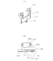
また、特許文献1に、別の電子部品ホルダーが開示されている。図7(a)は電子部品ホルダーの斜視図、図7(b)はプリント配線基板に装着された電子部品ホルダーの断面図である。
【0007】
この電子部品ホルダーは、電子部品108のリードフレーム109の直径の2倍以上の幅を有する腕部110を、ホルダー本体111の両側に形成し、この腕部110の先端にリードフレーム109を把む把持部112を設けるとともに、ホルダー本体111の中央の、腕部110と反対側に、プリント配線基板113のホルダー取付孔114に挿通して固定する脚部115を設けてなるもので、電子部品108のリードフレーム109をホルダー本体111の方向に折り曲げた後、リードフレーム109はプリント配線基板113の電子部品取付孔116に、脚部115はホルダー取付孔114にそれぞれ挿入し、リードフレーム109と配線回路とをはんだ117で接続している。
【0008】
【特許文献1】
特開昭61−59796号公報(第2頁左下欄第5行−第18行、第2図、第3図)
【0009】
【発明が解決しようとする課題】
ところが、図6に示す電子部品ホルダーでは、あらかじめ専用の治具を用いた別工程のフォーミング加工をする必要がある。リードフレームをリード保持穴に挿入して、カバー部材をホルダー本体に嵌着させることにより、リードフレームの基部を押さえつけてフォーミング加工することができるが、このようにすると、リードフレームの基部の位置があらかじめ定まっていないため、電子部品の位置ずれを生じさせるおそれがある。また、フォーミング加工時にリードフレームの根元に負荷がかかって、電子部品に不具合を生じさせたりするおそれがある。
【0010】
また、図7に示す電子部品ホルダーでは、例え、装着前に折り曲げたとしても、リードフレームの下端の位置が定まらず、ホルダー本体の脚部とリードフレームとを同時にプリント配線基板に装着するのが難しくなる。
【0011】
本発明は、電子部品を所定の高さおよび位置に保持すると共に、リードフレームを位置決めでき、かつ、リードフレームの根元に負荷をかけることなく、専用の治具を要する別工程のフォーミング加工を省略することができる電子部品ホルダーを提供することを目的とする。
【0012】
【課題を解決するための手段】
上記目的を達成するため、本発明は、プリント配線基板から所定の高さに電子部品を実装するための構造を前提として、リードフレームを位置決めするための機能と、リードフレームの根元に負荷をかけることなくフォーミング加工可能な治具としての機能とを備えた電子部品ホルダーを提供するものである。
【0013】
電子部品およびそのリードフレームの基部を所定の高さに保持するホルダー本体と、電子部品のリードフレームの中間部を係合してホルダー本体に嵌着されるカバー部材とを備える。カバー部材にリードフレームを係合して、そのカバー部材をホルダー本体に嵌着することにより、リードフレームをフォーミング加工可能とする。
【0014】
この構成によれば、リードフレームの基部をホルダー本体で保持しておき、リードフレームをフォーミング加工するので、リードフレームの根元に負荷がかからないようにすることができる。リードフレームを係合したカバー部材をホルダー本体に嵌着することにより、リードフレームをフォーミング加工することができる。カバー部材の嵌着後は、リードフレームの中間部を保持して位置決めすることができる。
【0015】
カバー部材とホルダー本体とをヒンジを介して一体的に形成し、カバー部材をヒンジの周りに回動させることにより、ホルダー本体に嵌着可能とする。そうすれば、リードフレームのフォーミング加工を伴うカバー部材の嵌着を簡単にすることができる。
【0016】
ホルダー本体を複数の電子部品を保持可能に形成し、このカバー部材をホルダー本体に嵌着することにより、複数の電子部品のリードフレームを同時にフォーミング加工可能とする。そうすれば、プリント配線基板に複数の電子部品を実装するとき、そのリードフレームのフォーミング加工を簡単にすることができる。
【0017】
ホルダー本体のリードフレームの基部を保持する保持部に、リードフレームの位置ずれを防止する位置ずれ防止手段を設ければ、リードフレームをフォーミング加工するときの位置ずれを防止して、電子部品を所定の位置に保持することができる。
【0018】
位置ずれ防止手段としては、リードフレームを挿入可能な挿入穴又は挿入溝で保持部を構成し、この保持部を屈曲状に形成してリードフレームを屈曲させる構成を例示できる。なお、他の構成としては、ホルダー本体との間にリードフレームを挟持する挟持部材を設けて、ホルダー本体とリードフレームとの摩擦によりリードフレームの位置ずれを防止する構造を例示できる。
【0019】
カバー部材に、ホルダー本体に嵌着するためのカバー用係合爪を設ければ、カバー部材のホルダー本体への嵌着を簡単かつ確実にすることができる。
【0020】
ホルダー本体を、前記電子部品とは別の第二電子部品を保持可能とすれば、例えばLEDとリードスイッチとを組み合わせて、プリント配線基板に実装することができ好適である。この場合、カバー部材に、ホルダー本体の座部との間に第二電子部品のリードを挟み込むための突起を形成すれば、ホルダー本体にカバー部材を嵌着することにより、電子部品のリードフレームをフォーミング加工すると共に第二電子部品のリードを固定することができる。
【0021】
【発明の実施の形態】
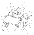
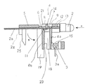
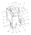
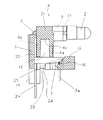
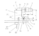
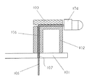
以下、本発明に係る電子部品ホルダーの実施の形態について、図面を用いて説明する。図1は本発明の電子部品ホルダーの斜視図(開状態)、図2はそのC−C断面図、図3は電子部品ホルダーの斜視図(閉状態)、図4はそのD−D断面図、図5はプリント配線基板に装着した電子部品ホルダーの側面図である。
【0022】
この電子部品ホルダーは、プリント配線基板1からの所定の高さおよび位置にLED(電子部品)2およびリードスイッチ(第二電子部品)3を実装するためのものであり、LED2およびリードスイッチ3を保持するホルダー本体4と、ホルダー本体4が保持するLED2のリードフレーム2aをフォーミング加工して保持するカバー部材5とを備えている。
【0023】
ホルダー本体4およびカバー部材5は、ヒンジ6を介して一体的に形成され、カバー部材5をヒンジ6の周りに回動させることにより、LED2を装着する開状態からリードフレーム2aを保持する閉状態に切り換え自在とされている。開状態から閉状態への切り換えにより、リードフレーム2aをフォーミング加工可能とされる。
【0024】
ホルダー本体4は、前板4a、後板4bおよび上板4cからなる断面略逆U形とされ、その上板4cの上面に、前方からLED2の二本のリードフレーム2aを挿入する二本の挿入溝7が形成されている。挿入溝7は、リードフレーム2aの基部を保持するようになっており、LED2を保持する保持部とされる。
【0025】
挿入溝7の溝壁は、両挿入溝7間に形成された内溝壁8と、内溝壁8の左右面に対向する二つの外溝壁9とからなり、挿入溝7に挿入されたリードフレーム2aの左右方向の移動を規制する。なお、内溝壁8の前方部分には、リードフレーム2aを挿入しやすくするためのテーパ10が形成されている。
【0026】
挿入溝7の深さは、ホルダー本体4の上板4cを貫通する深さに設定され、前板4aおよび後板4bの上端が、挿入溝7に挿入されたリードフレーム2aの下方への移動を規制する。なお、挿入溝7の後端である後板4bの上端には、リードフレーム2aの貫通を容易にするための面取り11が形成されている。
【0027】
左右の外溝壁9の前方部分を接続するように、挿入溝7の前部を跨ぐ前跨材12が設けられ、左右の外溝壁8の中央部分を接続するように、挿入溝7の中央付近を跨ぐ中跨材14が設けられている。この前跨材12および中跨材14により、リードフレーム2aの上方への移動が規制される。なお、前跨材12の左右方向における中央には、LED2を当てて位置決めするためのLED座13が突設されている。
【0028】
中跨材14は、その下面が挿入溝7に侵入する大きさに設定され、前板4a、後板4b、前跨材12および中跨材14により、挿入溝7に挿入されたリードフレーム2aを屈曲させる凹凸が構成される。この凹凸が、リードフレーム2aの位置ずれを防止する位置ずれ防止手段とされる。
【0029】
なお、リードフレーム2aの上方への移動を規制する前跨材12および中跨材14と、リードフレーム2aの下方への移動を規制する前板4aおよび後板4bとは、その前後方向の位置をずらして交互に形成され、上型および下型による成型が可能とされている。
【0030】
前板4aの下端には、前方に突出してリードスイッチ3を保持する第二保持部15が設けられている。第二保持部15には、リードスイッチ3のリード3aを配置するリード溝16が形成され、このリード溝16に、リード3aを下方に貫通させるリード貫通穴17が形成されている。これにより、リードスイッチ3を保持すると共に、リード3aをプリント配線基板1に接続可能とされる。
【0031】
ホルダー本体4の左右端は側板18で覆われ、この両側板18から下方に突出する脚部19に本体用係合爪20が形成されている。プリント配線基板1に形成されたホルダー取付孔(図示せず)に脚部19を挿入して本体用係合爪20を係合させることにより、電子部品ホルダーをプリント配線基板1に装着可能とされる。
【0032】
カバー部材5は、その左右方向およびこれに直交する方向の幅がホルダー本体4の前板4aおよび後板4bと等しい板状とされ、ホルダー本体4の後方に配されている。このカバー部材5は、開状態において、ホルダー本体4の上板4cと略同一平面に位置し、カバー部材5の前端と、ホルダー本体4の上板4cに突設されたヒンジ接続部21とが、薄板からなるヒンジ6を介して接続されている。ヒンジ6を屈曲させることにより、カバー部材5の下面とホルダー本体4の後板4bとが対向する閉状態に切換可能とされる。
【0033】
カバー部材5の下面には、リードフレーム2aを係合する二本のガイド溝22が形成されている。ガイド溝22は、開状態において、ホルダー本体4の挿入溝7の延長線上に位置し、挿入溝7を貫通したLED2のリードフレーム2aを侵入可能とされている。このガイド溝22は、フォーミング加工するときのリードフレーム2aの横ずれを阻止し、閉状態においては、ホルダー本体4の後板4bとの間にリードフレーム2aの中間部を保持する。
【0034】
カバー部材5の左右端には、カバー用係合爪24が形成され、このカバー用係合爪24をホルダー本体4の側板18に形成された切欠23に係合するにより、カバー部材5をホルダー本体4に嵌着可能とされる。カバー部材5の左右端付近には、閉状態において前板4aおよび後板4bを貫通する突起25が形成され、この突起25と、ホルダー本体4のリード溝(座部)16との間にリードスイッチ3のリード3aを挟み込むようになっている。
【0035】
次に、この電子部品ホルダーを用いてプリント配線基板1にLED2を実装する手順を説明する。まず、図1および図2に示す開状態において、LED2のリードフレーム2aをホルダー本体4の前方から挿入溝7に挿入し、LED2がLED座13に当たるまで、図1および図2における矢印Aの方向に押し込む。リードフレーム2aは、挿入溝7の凹凸によって屈曲しながら、面取り11に沿って挿入溝7を貫通し、ガイド溝22に侵入してカバー部材5に係合する。
【0036】
ヒンジ6を屈曲させながらカバー部材5を図2における矢印Bの方向に回動させて、図3および図4に示す閉状態に切り換えることにより、リードフレーム2aをカバー部材5のガイド溝22でガイドしながらフォーミング加工する。このとき、リードフレーム2aの基部は、挿入溝7の凹凸によって屈曲しており、矢印Aと逆方向へのLED2の位置ずれが防止される。
【0037】
カバー用係合爪24をホルダー本体4の切欠23に係合させてカバー部材5をホルダー本体4に嵌着させる。これにより、ホルダー本体4の後板4bおよびカバー部材5のガイド溝22が、リードフレーム2aの中間部を保持してプリント配線基板1のリード取付孔(図示せず)に挿入可能に位置決めする。また、カバー部材5の突起25が、ホルダー本体4の前板4aおよび後板4bを貫通して、ホルダー本体4のリード溝16に挿入されたリードスイッチ3のリード3aを押さえ、その上下方向の浮き上がりを規制する。
【0038】
脚部19をプリント配線基板1のホルダー取付孔(図示せず)に挿入して本体用係合爪20を係合させる。これにより、図5に示すように、電子部品ホルダーがプリント配線基板1に装着され、位置決めされたリードフレーム2aおよびリード3aがプリント配線基板1のリード取付孔に挿入される。
【0039】
はんだ槽に浸漬してはんだ付けをすることにより、プリント配線基板1から高さ(a)、プリント配線基板1の縁端から外方への距離(c)の位置にLED2が実装され、プリント配線基板1から高さ(b)、プリント配線基板1の縁端から内方への距離(d)の位置にリードスイッチ3が実装される。
【0040】
上記構成によれば、ホルダー本体4によってLED2およびリードスイッチ3を保持し、カバー部材5によってリードフレーム2aをフォーミング加工することができる。また、フォーミング加工後には、ホルダー本体4の後壁4bとカバー部材5のガイド溝22とでリードフレーム2aの中間部を保持し、プリント配線基板1のリード取付孔に挿入可能に位置決めすることができる。
【0041】
これにより、一つの電子部品ホルダーに、LED2およびリードスイッチ3を保持する機能と、LED2のリードフレーム2aをフォーミング加工する機能と、フォーミング加工したリードフレーム2aを保持する機能とを備えることができる。ホルダー本体4をプリント配線基板1に装着することにより、LED2およびリードスイッチ3をプリント配線基板1から所定の高さおよび位置に実装することができる。
【0042】
リードフレーム2aの基部を保持する挿通溝7に凹凸を形成するので、リードフレーム2aをフォーミング加工するときのLED2の位置ずれを防止することができる。また、カバー部材5にガイド溝22を形成するので、リードフレーム2aをフォーミング加工するときのリードフレーム2aの横ずれを阻止することができる。
【0043】
カバー部材5に形成した突起25がホルダー本体4のリード溝16との間にリードスイッチ3のリード3aを押さえるので、リード3aの浮き上がりを規制することができる。これにより、はんだ槽に浸漬してはんだ付けをするとき、噴流等によるリードスイッチ3の浮きを防止することができる。
【0044】
なお、本発明は、上記の実施の形態に限定されるものではなく、本発明の範囲内において、適宜変更を加えることができる。例えば、ホルダー本体は、一つのLED2を保持可能に形成するだけでなく、複数のLED2を保持可能に形成して、カバー部材5をホルダー本体4に嵌着することにより、複数のLED2のリードフレーム2aを同時にフォーミング加工可能としてもよい。
【0045】
この場合、LED2の個数に応じて、ホルダー本体4に複数の挿入溝7を形成し、カバー部材5に複数のガイド溝22を形成すればよい。また、LED2の代わりに、他の電子部品を保持してもよく、リードスイッチ3を装着せずに、LED2だけを保持するようにしてもよい。
【0046】
ヒンジ6を薄板状に形成する代わりに、ピンを用いた構造にしてもよく、カバー部材5とホルダー本体4とをヒンジ6を介して一体的に形成する代わりに、カバー部材5およびホルダー本体4を別体のものとしてもよい。カバー部材5に、カバー用係合爪24を形成する代わりに、ビスなどを用いてホルダー本体4に嵌着させるようにしてもよい。ホルダー本体4に本体用係合爪20を形成する代わりに、ビスなどを用いてプリント配線基板1に装着するようにしてもよい。
【0047】
リードフレーム2aの基部の位置ずれを防止する位置ずれ防止手段として、ホルダー本体4の挿入溝7を屈曲状に形成する代わりに、別体の挟圧部材を設けて、挟圧部材およびホルダー本体4との摩擦により、リードフレーム2aの基部の位置ずれを防止するようにしてもよい。
【0048】
リードフレーム2aの基部を保持する保持部として、挿入溝の代わりに挿入孔を形成してもよく、カバー部材5のガイド溝22の代わりに、カバー部材5を貫通するガイド孔を形成してもよい。
【0049】
【発明の効果】
以上の説明から明らかなように、本発明では、電子部品を所定の高さに保持するホルダー本体と、電子部品のリードフレームの中間部を係合してフォーミング加工するカバー部材とで電子部品ホルダーを構成している。そのため、電子部品をホルダー本体で保持したまま、リードフレームの根元に負荷をかけることなくフォーミング加工することができる。
【0050】
その結果、治具などを用いた別工程によるフォーミング加工を省略することができ、電子部品をプリント配線基板に実装するための工数およびコストの低減を図ることができる。
【0051】
カバー部材のガイド溝やガイド穴にリードフレームを係合することにより、リードフレームの横ずれを規制して、容易かつ確実にフォーミング加工することができる。フォーミング加工後には、カバー部材をホルダー本体に嵌着させることによってリードフレームを保持するので、リードフレームをプリント配線基板への所定の取付位置に位置決めすることができる。
【0052】
リードフレームの基部を保持するためのホルダー本体の保持部を屈曲状にするので、電子部品のリードフレームを屈曲させて、フォーミング加工時の電子部品の位置ずれを防止することができる。また、ホルダー本体が第二電子部品を保持可能となっているので、LEDとリードスイッチなどの組み合わせて実装することができる。複数の電子部品を併設する場合には、そのリードフレームを同時にフォーミング加工することができる。
【図面の簡単な説明】
【図1】本発明の電子部品ホルダーの斜視図(開状態)
【図2】そのC−C断面図
【図3】電子部品ホルダーの斜視図(閉状態)
【図4】そのD−D断面図
【図5】プリント配線基板に装着した電子部品ホルダーの側面図
【図6】従来の電子部品ホルダーの断面図
【図7】従来の別の電子部品ホルダーで、(a)は電子部品ホルダーの斜視図、(b)はプリント配線基板に装着された電子部品ホルダーの断面図
【符号の説明】
1 プリント配線基板
2 LED
2a リードフレーム
3 リードスイッチ
3a リード
4 ホルダー本体
4a 前板
4b 後板
5 カバー部材
6 ヒンジ
7 挿入溝
11 面取り
12 前跨材
14 中跨材
15 第二保持部
16 リード溝
20 本体用係合爪
22 ガイド溝
24 カバー用係合爪
25 突起[0001]
TECHNICAL FIELD OF THE INVENTION
The present invention relates to an electronic component holder that holds an electronic component for mounting an electronic component such as an LED on a printed wiring board.
[0002]
[Prior art]
Generally, an electronic component such as an LED mounted on a printed wiring board is held at a predetermined height and position from the printed wiring board by an electronic component holder, and a lead frame is subjected to forming processing and connected to the printed wiring. ing.
[0003]
FIG. 6 shows an example of the electronic component holder. The electronic component holder includes a holder main body 102 mounted on a printed wiring board 101 and a cover member 103 fitted on the upper surface of the holder main body 102. A lead frame 105 of an electronic component (LED) 104 By interposing the base, the electronic component 104 is held at a predetermined height and position.
[0004]
The holder main body 102 has a lead holding hole 106 for holding an intermediate portion of the lead frame 105. The center axis of the lead holding hole 106 is set parallel to a direction perpendicular to the plate surface of the printed wiring board 101, and the inserted lead frame 105 is positioned so as to match the lead mounting hole 107 of the printed wiring board 101.
[0005]
In order to insert the lead frame 105 into the lead holding hole 106 while holding the electronic component 104, the lead frame 105 is subjected to a forming process. This forming process has been performed in advance using a dedicated jig or the like.
[0006]
Patent Document 1 discloses another electronic component holder. FIG. 7A is a perspective view of an electronic component holder, and FIG. 7B is a cross-sectional view of the electronic component holder mounted on a printed wiring board.
[0007]
In this electronic component holder, arm portions 110 having a width of at least twice the diameter of the lead frame 109 of the electronic component 108 are formed on both sides of the holder main body 111, and the lead frame 109 is gripped by the tip of the arm portion 110. A grip part 112 is provided, and a leg 115 is provided at the center of the holder main body 111 on the side opposite to the arm 110 to be inserted into and fixed to the holder mounting hole 114 of the printed wiring board 113. After bending the lead frame 109 in the direction of the holder main body 111, the lead frame 109 is inserted into the electronic component mounting hole 116 of the printed wiring board 113, and the leg 115 is inserted into the holder mounting hole 114, respectively. And are connected by solder 117.
[0008]
[Patent Document 1]
JP-A-61-59796 (page 2, lower left column, line 5 to line 18, FIG. 2, FIG. 3)
[0009]
[Problems to be solved by the invention]
However, in the electronic component holder shown in FIG. 6, it is necessary to perform a separate forming process using a dedicated jig in advance. By inserting the lead frame into the lead holding hole and fitting the cover member to the holder body, the base of the lead frame can be pressed and formed, but in this case, the position of the base of the lead frame is changed. Since it is not determined in advance, there is a possibility that the electronic component may be displaced. In addition, a load may be applied to the base of the lead frame during the forming process, which may cause a defect in the electronic component.
[0010]
Further, in the electronic component holder shown in FIG. 7, even if the electronic component holder is bent before mounting, the position of the lower end of the lead frame is not determined, and the leg of the holder main body and the lead frame are simultaneously mounted on the printed wiring board. It becomes difficult.
[0011]
The present invention holds the electronic component at a predetermined height and position, can position the lead frame, and does not apply a load to the root of the lead frame, and eliminates the forming process in a separate process requiring a dedicated jig. It is an object of the present invention to provide an electronic component holder that can perform the above operations.
[0012]
[Means for Solving the Problems]
In order to achieve the above object, the present invention provides a function for positioning a lead frame and a load on a root of the lead frame, assuming a structure for mounting an electronic component at a predetermined height from a printed wiring board. An object of the present invention is to provide an electronic component holder having a function as a jig that can be formed without forming.
[0013]
The electronic device includes a holder body that holds the base of the electronic component and its lead frame at a predetermined height, and a cover member that is fitted to the holder body by engaging an intermediate portion of the lead frame of the electronic component. The lead frame can be formed by engaging the lead frame with the cover member and fitting the cover member to the holder body.
[0014]
According to this configuration, since the base of the lead frame is held by the holder body and the lead frame is formed, a load can be prevented from being applied to the root of the lead frame. By fitting the cover member engaged with the lead frame to the holder body, the lead frame can be formed. After the cover member is fitted, the intermediate portion of the lead frame can be held and positioned.
[0015]
The cover member and the holder main body are integrally formed via a hinge, and the cover member is turned around the hinge so that it can be fitted to the holder main body. Then, the fitting of the cover member with the forming process of the lead frame can be simplified.
[0016]
The holder main body is formed so as to hold a plurality of electronic components, and the cover member is fitted to the holder main body, so that the lead frames of the plurality of electronic components can be formed simultaneously. Then, when a plurality of electronic components are mounted on the printed wiring board, the forming process of the lead frame can be simplified.
[0017]
If the holding portion for holding the base of the lead frame of the holder body is provided with a misalignment preventing means for preventing misalignment of the lead frame, misalignment when forming the lead frame can be prevented, and the electronic component can be predetermined. Position.
[0018]
Examples of the displacement prevention means include a configuration in which a holding portion is configured by an insertion hole or an insertion groove into which a lead frame can be inserted, and the holding portion is formed in a bent shape to bend the lead frame. As another configuration, a structure in which a holding member for holding the lead frame between the holder body and the holder body is provided to prevent the displacement of the lead frame due to friction between the holder body and the lead frame can be exemplified.
[0019]
If the cover member is provided with a cover engaging claw for fitting to the holder body, the cover member can be easily and securely fitted to the holder body.
[0020]
If the holder main body is capable of holding a second electronic component different from the electronic component, for example, an LED and a reed switch can be combined and mounted on a printed wiring board, which is preferable. In this case, if a projection for inserting the lead of the second electronic component between the cover member and the seat of the holder main body is formed, the lead frame of the electronic component can be formed by fitting the cover member to the holder main body. Forming can be performed and the lead of the second electronic component can be fixed.
[0021]
BEST MODE FOR CARRYING OUT THE INVENTION
Hereinafter, embodiments of an electronic component holder according to the present invention will be described with reference to the drawings. FIG. 1 is a perspective view of an electronic component holder of the present invention (open state), FIG. 2 is a cross-sectional view taken along line CC, FIG. 3 is a perspective view of the electronic component holder (closed state), and FIG. FIG. 5 is a side view of the electronic component holder mounted on the printed wiring board.
[0022]
This electronic component holder is for mounting an LED (electronic component) 2 and a reed switch (second electronic component) 3 at a predetermined height and position from the printed wiring board 1. It has a holder body 4 for holding, and a cover member 5 for holding the lead frame 2a of the LED 2 held by the holder body 4 by forming.
[0023]
The holder main body 4 and the cover member 5 are integrally formed via a hinge 6, and the cover member 5 is rotated around the hinge 6 to change the open state where the LED 2 is mounted to the closed state where the lead frame 2 a is held. It can be switched freely. By switching from the open state to the closed state, the lead frame 2a can be formed.
[0024]
The holder main body 4 has a substantially inverted U-shaped cross section including a front plate 4a, a rear plate 4b, and an upper plate 4c. Two lead frames 2a of the LED 2 are inserted into the upper surface of the upper plate 4c from the front. An insertion groove 7 is formed. The insertion groove 7 holds the base of the lead frame 2a, and serves as a holding unit for holding the LED 2.
[0025]
The groove wall of the insertion groove 7 includes an inner groove wall 8 formed between the two insertion grooves 7, and two outer groove walls 9 facing the left and right surfaces of the inner groove wall 8, and is inserted into the insertion groove 7. The movement of the lead frame 2a in the left-right direction is restricted. In addition, a taper 10 is formed in a front portion of the inner groove wall 8 to facilitate insertion of the lead frame 2a.
[0026]
The depth of the insertion groove 7 is set to a depth penetrating the upper plate 4c of the holder body 4, and the upper ends of the front plate 4a and the rear plate 4b move downward of the lead frame 2a inserted into the insertion groove 7. Regulate. A chamfer 11 for facilitating the penetration of the lead frame 2a is formed at the upper end of the rear plate 4b, which is the rear end of the insertion groove 7.
[0027]
A front straddle member 12 that straddles the front portion of the insertion groove 7 is provided so as to connect the front portions of the left and right outer groove walls 9. A middle straddle 14 is provided to straddle the vicinity of the center. The upward movement of the lead frame 2a is regulated by the front straddling member 12 and the middle straddling member 14. An LED seat 13 for projecting and positioning the LED 2 is provided at the center of the front straddle 12 in the left-right direction.
[0028]
The middle straddle 14 is set to have a size such that the lower surface thereof enters the insertion groove 7, and the lead frame 2 a inserted into the insertion groove 7 by the front plate 4 a, the rear plate 4 b, the front straddle 12 and the middle straddle 14. Is formed. The unevenness serves as a position shift preventing means for preventing the position shift of the lead frame 2a.
[0029]
The front straddling member 12 and the middle straddling member 14 that regulate the upward movement of the lead frame 2a and the front plate 4a and the rear plate 4b that regulate the downward movement of the lead frame 2a are positioned in the front-rear direction. Are formed alternately so that molding by an upper die and a lower die is possible.
[0030]
At the lower end of the front plate 4a, a second holding portion 15 that projects forward and holds the reed switch 3 is provided. In the second holding portion 15, a lead groove 16 for disposing the lead 3a of the reed switch 3 is formed, and a lead through hole 17 for penetrating the lead 3a downward is formed in the lead groove 16. As a result, the lead switch 3 can be held and the lead 3 a can be connected to the printed wiring board 1.
[0031]
The left and right ends of the holder body 4 are covered with side plates 18, and main body engaging claws 20 are formed on legs 19 projecting downward from the side plates 18. The electronic component holder can be mounted on the printed wiring board 1 by inserting the legs 19 into the holder mounting holes (not shown) formed in the printed wiring board 1 and engaging the main body engaging claws 20. You.
[0032]
The cover member 5 is formed in a plate shape having the same width in the left-right direction and in the direction orthogonal thereto as the front plate 4a and the rear plate 4b of the holder body 4, and is arranged behind the holder body 4. In the open state, the cover member 5 is located on substantially the same plane as the upper plate 4c of the holder body 4, and the front end of the cover member 5 and the hinge connection portion 21 protruding from the upper plate 4c of the holder body 4 are provided. , Are connected via a hinge 6 made of a thin plate. By bending the hinge 6, it is possible to switch to a closed state in which the lower surface of the cover member 5 and the rear plate 4b of the holder main body 4 face each other.
[0033]
On the lower surface of the cover member 5, two guide grooves 22 for engaging the lead frame 2a are formed. The guide groove 22 is located on an extension of the insertion groove 7 of the holder body 4 in the open state, and is capable of entering the lead frame 2 a of the LED 2 that has penetrated the insertion groove 7. The guide groove 22 prevents lateral displacement of the lead frame 2a at the time of forming processing, and holds the intermediate portion of the lead frame 2a between the holder frame 4 and the rear plate 4b in the closed state.
[0034]
At the left and right ends of the cover member 5, cover engaging claws 24 are formed, and the cover engaging claws 24 are engaged with the cutouts 23 formed on the side plates 18 of the holder body 4, so that the cover member 5 is held by the holder. It can be fitted to the main body 4. Protrusions 25 are formed near the left and right ends of the cover member 5 so as to penetrate the front plate 4a and the rear plate 4b in the closed state, and a lead is provided between the protrusion 25 and the lead groove (seat portion) 16 of the holder body 4. The lead 3a of the switch 3 is sandwiched therebetween.
[0035]
Next, a procedure for mounting the LED 2 on the printed wiring board 1 using the electronic component holder will be described. First, in the open state shown in FIGS. 1 and 2, the lead frame 2 a of the LED 2 is inserted into the insertion groove 7 from the front of the holder body 4, and the direction of the arrow A in FIGS. Press The lead frame 2 a penetrates the insertion groove 7 along the chamfer 11, enters the guide groove 22 and engages with the cover member 5 while being bent by the unevenness of the insertion groove 7.
[0036]
By rotating the cover member 5 in the direction of arrow B in FIG. 2 while bending the hinge 6 and switching to the closed state shown in FIGS. 3 and 4, the lead frame 2 a is guided by the guide groove 22 of the cover member 5. Forming while doing. At this time, the base of the lead frame 2a is bent by the unevenness of the insertion groove 7, and the displacement of the LED 2 in the direction opposite to the arrow A is prevented.
[0037]
The cover engaging member 24 is fitted to the holder main body 4 by engaging the cover engaging claw 24 with the notch 23 of the holder main body 4. Thus, the rear plate 4b of the holder body 4 and the guide groove 22 of the cover member 5 hold the intermediate portion of the lead frame 2a and position the lead frame 2a so that it can be inserted into the lead mounting hole (not shown) of the printed wiring board 1. Further, the projection 25 of the cover member 5 penetrates through the front plate 4a and the rear plate 4b of the holder main body 4 and presses the lead 3a of the reed switch 3 inserted into the lead groove 16 of the holder main body 4. Regulate lift.
[0038]
The legs 19 are inserted into holder mounting holes (not shown) of the printed wiring board 1 to engage the main body engaging claws 20. As a result, as shown in FIG. 5, the electronic component holder is mounted on the printed wiring board 1, and the positioned lead frame 2a and lead 3a are inserted into the lead mounting holes of the printed wiring board 1.
[0039]
By immersing in the solder bath and performing soldering, the LED 2 is mounted at a height (a) from the printed wiring board 1 and at a distance (c) from the edge of the printed wiring board 1 to the outside. The reed switch 3 is mounted at a height (b) from the board 1 and at a distance (d) from the edge of the printed wiring board 1 to the inside.
[0040]
According to the above configuration, the LED 2 and the reed switch 3 are held by the holder body 4, and the lead frame 2 a can be formed by the cover member 5. Further, after the forming process, the intermediate portion of the lead frame 2a is held by the rear wall 4b of the holder body 4 and the guide groove 22 of the cover member 5, and is positioned so that it can be inserted into the lead mounting hole of the printed wiring board 1. it can.
[0041]
Thus, one electronic component holder can have a function of holding the LED 2 and the reed switch 3, a function of forming the lead frame 2a of the LED 2, and a function of holding the formed lead frame 2a. By mounting the holder body 4 on the printed wiring board 1, the LED 2 and the reed switch 3 can be mounted at a predetermined height and position from the printed wiring board 1.
[0042]
Since irregularities are formed in the insertion groove 7 that holds the base of the lead frame 2a, it is possible to prevent the LED 2 from being displaced when forming the lead frame 2a. Further, since the guide groove 22 is formed in the cover member 5, it is possible to prevent a lateral displacement of the lead frame 2a when forming the lead frame 2a.
[0043]
Since the protrusion 25 formed on the cover member 5 presses the lead 3a of the reed switch 3 between the protrusion 25 and the lead groove 16 of the holder body 4, the lifting of the lead 3a can be restricted. This makes it possible to prevent the reed switch 3 from floating due to a jet or the like when soldering by immersion in a solder bath.
[0044]
It should be noted that the present invention is not limited to the above-described embodiment, and can be appropriately modified within the scope of the present invention. For example, the holder main body is formed so as to be able to hold one LED 2 as well as a plurality of LEDs 2, and the cover member 5 is fitted to the holder main body 4, so that the lead frame of the plurality of LEDs 2 is formed. 2a may be formed simultaneously.
[0045]
In this case, a plurality of insertion grooves 7 may be formed in the holder body 4 and a plurality of guide grooves 22 may be formed in the cover member 5 according to the number of the LEDs 2. Further, instead of the LED 2, another electronic component may be held, and only the LED 2 may be held without mounting the reed switch 3.
[0046]
Instead of forming the hinge 6 in a thin plate shape, a structure using a pin may be used. Instead of integrally forming the cover member 5 and the holder body 4 via the hinge 6, the cover member 5 and the holder body 4 may be used. May be separate. Instead of forming the cover engaging claw 24 on the cover member 5, the cover member 5 may be fitted to the holder body 4 using screws or the like. Instead of forming the main body engaging claws 20 on the holder main body 4, the main body engaging claws 20 may be mounted on the printed wiring board 1 using screws or the like.
[0047]
As means for preventing displacement of the base of the lead frame 2a, instead of forming the insertion groove 7 of the holder body 4 in a bent shape, a separate clamping member is provided, and the clamping member and the holder body 4 are provided. , The displacement of the base of the lead frame 2a may be prevented.
[0048]
As a holding portion for holding the base of the lead frame 2a, an insertion hole may be formed instead of the insertion groove, and a guide hole penetrating the cover member 5 may be formed instead of the guide groove 22 of the cover member 5. Good.
[0049]
【The invention's effect】
As is apparent from the above description, in the present invention, the electronic component holder includes the holder body that holds the electronic component at a predetermined height and the cover member that engages with the middle part of the lead frame of the electronic component and forms the workpiece. Is composed. Therefore, the forming process can be performed without applying a load to the root of the lead frame while holding the electronic component by the holder body.
[0050]
As a result, forming by a separate process using a jig or the like can be omitted, and the man-hour and cost for mounting the electronic component on the printed wiring board can be reduced.
[0051]
By engaging the lead frame with the guide groove or the guide hole of the cover member, the lateral displacement of the lead frame is regulated, and the forming process can be performed easily and reliably. After the forming process, the lead frame is held by fitting the cover member to the holder body, so that the lead frame can be positioned at a predetermined mounting position on the printed wiring board.
[0052]
Since the holding portion of the holder main body for holding the base of the lead frame is bent, the lead frame of the electronic component can be bent, and the displacement of the electronic component at the time of forming can be prevented. In addition, since the holder body can hold the second electronic component, it can be mounted in combination with an LED and a reed switch. When a plurality of electronic components are provided side by side, the lead frames can be formed simultaneously.
[Brief description of the drawings]
FIG. 1 is a perspective view of an electronic component holder of the present invention (in an open state).
FIG. 2 is a cross-sectional view taken along the line CC. FIG. 3 is a perspective view of the electronic component holder (closed state).
FIG. 4 is a cross-sectional view taken along a line D-D. FIG. 5 is a side view of an electronic component holder mounted on a printed wiring board. FIG. 6 is a cross-sectional view of a conventional electronic component holder. And (a) is a perspective view of the electronic component holder, and (b) is a cross-sectional view of the electronic component holder mounted on the printed wiring board.
1 printed wiring board 2 LED
2a Lead frame 3 Lead switch 3a Lead 4 Holder body 4a Front plate 4b Rear plate 5 Cover member 6 Hinge 7 Insertion groove 11 Chamfer 12 Front straddle material 14 Middle straddle material 15 Second holding unit 16 Lead groove 20 Main body engaging claw 22 Guide groove 24 Engagement claw 25 for cover Projection