JP2004276177A - Minutely machining apparatus - Google Patents
Minutely machining apparatus Download PDFInfo
- Publication number
- JP2004276177A JP2004276177A JP2003072051A JP2003072051A JP2004276177A JP 2004276177 A JP2004276177 A JP 2004276177A JP 2003072051 A JP2003072051 A JP 2003072051A JP 2003072051 A JP2003072051 A JP 2003072051A JP 2004276177 A JP2004276177 A JP 2004276177A
- Authority
- JP
- Japan
- Prior art keywords
- cantilever
- probe
- workpiece
- mounting member
- cantilevers
- Prior art date
- Legal status (The legal status is an assumption and is not a legal conclusion. Google has not performed a legal analysis and makes no representation as to the accuracy of the status listed.)
- Granted
Links
Images


Landscapes
- Length Measuring Devices With Unspecified Measuring Means (AREA)
- Micromachines (AREA)
Abstract
Description
【0001】
【発明の属する技術分野】
この発明は、原子間力顕微鏡の原理を利用した、ナノメートルオーダーの加工や素子の作製のための微細加工装置に関する。
【0002】
【従来の技術】
【特許文献1】特開2001−246600号公報
【特許文献2】特開2002−14024号公報
【特許文献3】特開2002−154100号公報
近年超精密加工技術が発達し、機械加工においてもマイクロメータレベルの機械加工が存在している。しかし、今日の電子機器におけるICや素子などの高集積化やマイクロマシン等の製造において、より微細な加工技術が求められている。そのような情勢の中で、ナノメートルオーダーから原子分解能を有する原子間力顕微鏡(AFM)や走査型トンネル顕微鏡(STM)といった走査型プローブ顕微鏡(SPM)を応用した微細加工の研究が行われている。
【0003】
例えば特許文献3に開示されている微細加工装置は、弾性体に支持され少なくとも先端に導電性部分を有する探針を、被加工物表面に対向させ、この探針を被加工物表面と平行な方向に相対的に移動させ、探針先端の導電性部分と被加工物の間に電圧を印加して、被加工物に微細加工を施すものである。被加工物は、探針先端から被加工物に電流が流れることにより、形状、導電率、屈折率、電気分極率などの物性や構造が変化するものである。
【0004】
特許文献3の微細加工装置は、試料台をピエゾ素子により駆動して、探針に対して任意の方向に任意の距離移動させることが可能である。さらに、探針を支持した弾性体をその共振周波数近傍の振動数で被加工物表面に対して垂直方向に振動させ、被加工物表面上の凹凸構造による、探針と被加工物表面の距離のずれによる弾性体の共振周波数のずれの信号を制御装置へフィードバックして、探針と被加工物表面間の距離を一定に保つものである。
【0005】
【発明が解決しようとする課題】
上記従来の技術の特許文献3に記載された微細加工装置は、探針から被加工物に電流を流して、被加工物の物性を変化させて加工を行うもので、純粋な機械加工を行うことができるものではない。また、加工を施した部分の加工状態や形状を簡単に知ることができるものではなく、一定の加工が終了した後、被加工物を原子間力顕微鏡等にセットし直して加工状態を確認しなければならないものであり、加工の修正や追加工等を簡単に行うことができるものではない。
【0006】
この発明は、上記従来の技術の問題点に鑑みてなされたものであり、簡単な構成で、超微細寸法の機械加工を行うことができ、可搬性があり、加工対象を選ばない微細加工装置を提供することを目的とする。
【0007】
【課題を解決するための手段】
この発明は、被加工物に接触して加工を行う角錐状ダイヤモンドバルクチップ等の第一の探針と、この探針が固定された第一のカンチレバーと、被加工物に接近してその形状や物性その他の性状を検知する探針であって、角錐状のシリコン系材料のチップにダイヤモンドコーティングした第二の探針と、この第二の探針が固定された第二のカンチレバーと、これら第一、第二のカンチレバーを所定間隔空けて保持したカンチレバー取付部材とを備えた微細加工装置である。そして、このカンチレバー取付部材を移動自在に保持した支持部材と、この支持部材とともに上記第一、第二のカンチレバーを任意の方向に微小駆動する圧電駆動装置と、上記第一、第二のカンチレバーの各探針の変位を検知する光学的検知装置と、上記圧電駆動装置を作動させて上記支持部材を介して上記第一のカンチレバーを微小変位させ上記第一の探針により被加工物を機械加工する加工制御手段と、上記第二の探針及び上記光学的検知装置により被加工物の表面を測定する計測制御手段とを備え、上記カンチレバー取付部材を移動させて上記第一、第二のカンチレバーの位置を切り替え可能に設けた微細加工装置である。
【0008】
上記圧電駆動装置は本体ケースに固定され、上記第一、第二のカンチレバーは上記圧電駆動装置により、上記本体ケースに対して微小変位可能に設けられている。また、上記カンチレバー取付部材を、上記第一、第二の探針の先端から等距離の回動軸であって上記第一、第二の探針の先端を含む面に対して直角な回動軸で回転自在に設け、上記カンチレバー取付部材を回動させて上記第一、第二のカンチレバーの位置を切り替えるカンチレバー切換装置を備えたものである。上記カンチレバー切換装置は、駆動用のモータと、ウォームホイール機構等により構成しても良い。
【0009】
上記支持部材は、上記被加工物の設置面に対して上記カンチレバー取付部材を僅かに斜めに位置決めして支持し、上記回動軸も上記被加工物の設置面に立てた垂線に対して僅かに傾斜して設けられ、上記被加工物に一方の上記探針が接する状態で、他方の探針は上記被加工物の設置面から離れた退避位置に位置決めされるものである。
【0010】
上記光学的検知装置は、半導体レーザー素子と、この半導体レーザー素子からの光を上記第一または第二のカンチレバー上に導く光学系と、上記カンチレバーに照射されたレーザー光の反射光を検知するとともに上記カンチレバーの変位を検知する4分割フォトダイオード等の光検知素子と、上記カンチレバーに照射されたレーザー光の反射光を上記光検知素子に導く光学系とから成る。
【0011】
この発明の微細加工装置は、第一、第二の探針を切り換え可能に設け、第一の探針で加工を行い、第一、第二の探針を切り換えて、その加工状態を第二の探針で簡単に測定できるようにしたものである。また、第一、第二探針を保持した第一、第二のカンチレバー及びそのカンチレバー取付部材を圧電駆動装置により駆動可能に設け、被加工物を固定した状態で、任意の微細加工を行うことができるようにしたものである。
【0012】
【発明の実施の形態】
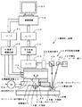
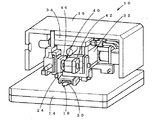
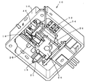
以下、この発明の実施形態について図面に基づいて説明する。図1〜図4はこの発明の一実施形態を示すもので、この実施形態の微細加工装置10は、図示するように、被加工物12が載せられた定盤14に設置可能なもので、一側面が開口した金属製の箱状の本体ケース16に設けられている。本体ケース16内には、被加工物12に接触して加工を行う角錐状のダイヤモンドバルクチップ等の第一の探針18と、この探針が固定された第一のカンチレバー20、及び被加工物12に接近してその形状や物性その他の性状を検知する探針であって、角錐状のシリコン系材料のチップにダイヤモンドコーティングした第二の探針19と、この第二の探針19が固定された第二のカンチレバー21とを有する。第一、第二のカンチレバー20,21は、互いに90°の角度を成して延出し、この第一、第二のカンチレバー20,21を保持したカンチレバー取付部材24が本体ケース16内に設けられている。
【0013】
カンチレバー取付部材24は、第一、第二の探針18,19の先端から等距離の位置にある軸であって第一、第二の探針18,19の先端を含む仮想の面に対して直角な回動軸26で回動自在に軸支されている。この回動軸26とカンチレバー取付部材24との間には、ベアリング28が設けられている。また、回動軸26は、固定部材30に固定され、回動軸26と固定部材30により、カンチレバー取付部材24の支持部材を構成している。固定部材30の取付面30aは、図1に示すように、カンチレバー取付部材24を定盤14の表面に対して僅かに斜めに位置決めし、回動軸26も、定盤14の表面に立てた垂線に対して僅かに傾斜して設けられている。そして、本体ケース16に設けられた状態で、被加工物12に第一または第二の探針18または19が接する状態で、他方の探針19または18は定盤12から僅かに離れた退避位置に位置決めされるように設けられている。
【0014】
固定部材30は、図示しない圧電素子を備えた圧電駆動装置32に固定されている。圧電駆動装置32は、互いに直角な方向であるXYZ方向に固定部材を変位させ、カンチレバー取付部材24を介して、第一、第二のカンチレバー20,21を任意の方向に微小変位させる。圧電駆動装置32は、位置決めステージ34に固定され、位置決めステージ34は本体ケース16の内面である天井面16aに固定されている。
【0015】
第一、第二のカンチレバー20,21の所定の加工計測位置には、第一、第二の探針18,19の変位を検知する光学的検知装置40が、本体ケース16内に設けられている。光学的検知装置40は、レーザーダイオードである半導体レーザー素子42と、この半導体レーザー素子42からのレーザー光を所定の加工計測位置の、第一または第二のカンチレバー20または21上に導くミラーやその他図示しないレンズから成る光学系44を備えている。さらに、光学的検知装置40は、第一または第二のカンチレバー20または21上に照射されたレーザー光の反射光を検知するとともに、その第一または第二のカンチレバー20または21の変位を検知する4分割フォトダイオードから成る光検知素子46と、第一または第二のカンチレバー20または21に照射されたレーザー光の反射光を、光検知素子46に導くプリズムやその他図示しないレンズから成る光学系48とを備えている。
【0016】
光検知素子46の出力は、電流/電圧変換回路50を介して信号処理回路52に接続されている。信号処理回路52では、4分割フォトダイオードの光検知素子46からの出力を処理して、第一または第二のカンチレバー20または21の変位を計測可能な信号にする。信号処理回路52の出力は、A/D変換器54によりアナログ信号をディジタル信号に変換されて、コンピュータである制御装置56に入力する。制御装置56には、モニタ58が接続され、さらに、制御装置56の制御信号出力は、D/A変換器60を介して、ディジタル信号がアナログ信号に変換されて、圧電駆動装置32の圧電素子を駆動する圧電素子駆動回路に入力している。
【0017】
コンピュータである制御装置56は、内部に所定のプログラムを有し、圧電駆動装置32を作動させて第一カンチレバー20を微小変位させ、第一の探針18により被加工物12を機械加工する加工制御手段と、第二のカンチレバー21を微小変位させ、第二の探針19により被加工物12の表面を検知し、光学的検知装置40により被加工物12の表面を測定する計測制御手段とを兼ねている。
【0018】
また、カンチレバー取付部材24は、本体ケース16内の図示しないウォームホイール機構を介して、本体ケース16内に固定されたモータ64に接続されている。モータ64は、制御装置56からの指示により、カンチレバー取付部材24を90°回動させ、第一、第二のカンチレバー20,21の位置を任意に切り替える。
【0019】
この実施形態の微細加工装置の動作は、定盤14上に被加工物12を載置し、先ず加工用の第一の探針18により被加工物12の所定位置に微細加工を施す。この微細加工は、制御装置56により被加工物12の表面上で探針18が所定の圧力で所定の動きをするように、圧電素子駆動回路62を介して圧電駆動装置32を動作させる。これにより、固定部材30を経てカンチレバー取付部材24が駆動され、第一のカンチレバー20が微小変位し、先端の探針18が微細に移動する。この探針18の移動により、ダイヤモンドチップ等の探針18の先端により被加工物12の表面が切削され、ナノメートルオーダーの加工が成される。この加工は、制御装置56により3次元的にXYZ方向に制御される。加工データは、第一のカンチレバー20のたわみとして光学的検知装置40により検出される。この検出は、第一のカンチレバー20の加工時の力により第一のカンチレバー20の上面に僅かなたわみが生じ、このたわみにより半導体レーザー素子42からのレーザー光の反射光の位置が僅かにずれ、この反射光の変化を4分割フォトダイオードによる光検知素子46により検知し、信号処理回路52等を介して制御装置56にフィードバックされる。これにより、所定の形状の微細加工が行われる。
【0020】
次に、微細加工の途中または終了後に、モータ64によりカンチレバー取付部材24を90°回動させて第一の探針18を退避位置に位置させるとともに、第二の探針19を被加工物12の微細加工箇所上に位置させる。この回動時には、第一、第二の探針18,19を、圧電駆動装置32等により被加工物12の表面よりも上方に対比させて回動する。そして、計測用の第二の探針19を、加工を施した箇所に接触させ、制御装置56により被加工物12の表面形状を検知する。この計測は、従来の原子間力顕微鏡と同様である。このときも、第二探針19の位置変化を第二のカンチレバー21に照射されたレーザー光の反射光の位置により検知し、被加工物12の表面形状を計測する。
【0021】
この実施形態の微細加工装置10は、第一、第二の探針18,19が切り換え可能に設けられ、第一の探針18で微細な加工を行い、その加工状態を第二の探針19で簡単に計測することができる。これにより、加工後に加工状態を迅速に測定することができ、より微細な加工や複雑な加工も行うことができ、被加工物12の材質も問わないものである。さらに、装置全体がケース本体16内に設けられ、可搬性が高く、被加工物12の場所や位置を問わず微細加工を行うことができる。
【0022】
なお、この発明の微細加工装置は、上記実施形態に限定されるものではなく図5に示すように、カンチレバー取付部材24は、微細加工用の第一の探針18を保持した第一のカンチレバー20と、計測用の第二の探針19を保持した第二のカンチレバー21の他、さらに、他の加工を行う加工工具70を第二のカンチレバー21に対し回動軸26を中心に、180°反対側に設けても良い。この位置に設ける加工工具70としては、例えば、ナノメートルオーダーの切削加工を行うことができるフライス装置72である。このフライス装置72の加工工具70の先端には、第一の探針18と同様に、ダイヤモンドバルクチップ等の微細加工用チップ74が固定される。またこのフライス装置72の加工工具70は、超小型モータ76の回転軸に接続され、この超小型モータ76がカンチレバーまたはカンチレバー取付部材24に設けられている。この超小型のフライス装置72によれば、広い範囲で微細な切削加工を行うことができる。
【0023】
また、加工工具70以外の測定用探針や加工工具をさらに付加しても良く、カンチレバー取付部材に直接または間接的に設けられる探針や工具の数は適宜設定することができる。
【0024】
さらに、カンチレバー取付部材の移動方向は、回動以外に一定方向に摺動するようにしたものでも良い。第一、第二の探針等は摺動によっても同様に切り替えることができ、同様の効果を得ることができる。また、第一、第二のカンチレバーに設けられる探針は、ダイヤモンドバルクチップ以外に微細加工が可能な工具であれば良く、加工は切削加工のみならず塑性加工も可能であり、切削加工の形態も問わないものである。さらに、探針と被加工物との間に通電しながら加工を行うものでも良く、加工環境や雰囲気は問わない。
【0025】
【発明の効果】
この発明の微細加工装置は、簡単な構造で、加工と計測を適宜切り替えることができ、より微細な加工を高精度に行うことができる。また、被加工物の材質を選ばず微細な加工が可能である。さらに、装置がケース本体内に設けられているので、可搬性が高く、任意の場所での微細加工が可能となる。
【図面の簡単な説明】
【図1】この発明の一実施形態の微細加工装置の概略ブロック図である。
【図2】この実施形態の微細加工装置の部分破断斜視図である。
【図3】この実施形態の微細加工装置の光学的検知装置を示す部分破断斜視図である。
【図4】この実施形態の微細加工装置の背面を示す斜視図である。
【図5】この発明の微細加工装置の他の実施形態の背面を示す斜視図である。
【符号の説明】
10 微細加工装置
12 被加工物
14 定盤
16 本体ケース
18 第一の探針
19 第二の探針
20 第一のカンチレバー
21 第二のカンチレバー
24 カンチレバー取付部材
26 回動軸
30 固定部材
32 圧電駆動装置
40 光学的検知装置
42 半導体レーザー素子
46 光検知素子
56 制御装置
62 圧電素子駆動回路[0001]
TECHNICAL FIELD OF THE INVENTION
The present invention relates to a microfabrication apparatus for processing on the order of nanometers and manufacturing elements using the principle of an atomic force microscope.
[0002]
[Prior art]
[Patent Document 1] Japanese Patent Application Laid-Open No. 2001-246600 [Patent Document 2] Japanese Patent Application Laid-Open No. 2002-14024 [Patent Document 3] Japanese Patent Application Laid-Open No. 2002-154100 Meter-level machining exists. However, in today's electronic devices, higher integration of ICs and elements, and manufacture of micromachines and the like require finer processing techniques. Under such circumstances, research on fine processing using a scanning probe microscope (SPM), such as an atomic force microscope (AFM) or a scanning tunnel microscope (STM) having an atomic resolution from the order of nanometers, has been conducted. I have.
[0003]
For example, a microfabrication device disclosed in
[0004]
The microfabrication device disclosed in
[0005]
[Problems to be solved by the invention]
The micromachining device described in
[0006]
The present invention has been made in view of the above-mentioned problems of the conventional technology, and has a simple configuration, can perform machining of ultra-fine dimensions, is portable, and has a portable and micro-processing apparatus that does not select a processing object. The purpose is to provide.
[0007]
[Means for Solving the Problems]
The present invention relates to a first probe such as a pyramid-shaped diamond bulk tip that performs processing by contacting a workpiece, a first cantilever to which the probe is fixed, and a shape close to the workpiece. And a second tip, which is a diamond-coated tip of a pyramidal silicon-based material, a second cantilever to which the second tip is fixed, And a cantilever mounting member holding the first and second cantilevers at predetermined intervals. And, a support member that movably holds the cantilever mounting member, a piezoelectric drive device that minutely drives the first and second cantilevers in an arbitrary direction together with the support member, and a first and second cantilever. An optical detection device for detecting the displacement of each probe, and the piezoelectric drive device is operated to finely displace the first cantilever through the support member, and machine the workpiece with the first probe. Processing control means, and measurement control means for measuring the surface of the workpiece by the second probe and the optical detection device, the first and second cantilevers by moving the cantilever mounting member Is a micromachining device provided so that the position of the micromachining can be switched.
[0008]
The piezoelectric driving device is fixed to a main body case, and the first and second cantilevers are provided to be slightly displaceable with respect to the main body case by the piezoelectric driving device. Further, the cantilever mounting member is rotated at a right angle to a plane including a tip of the first and second probes, which is a rotation axis equidistant from tips of the first and second probes. A cantilever switching device is provided rotatably on a shaft, and switches the position of the first and second cantilevers by rotating the cantilever mounting member. The cantilever switching device may include a driving motor, a worm wheel mechanism, and the like.
[0009]
The support member supports the cantilever mounting member by positioning the cantilever mounting member slightly obliquely with respect to the installation surface of the workpiece, and the rotation axis is also slightly inclined with respect to a vertical line set on the installation surface of the workpiece. The other probe is positioned at a retracted position away from the installation surface of the workpiece while one of the probes is in contact with the workpiece.
[0010]
The optical detection device is a semiconductor laser element, an optical system that guides light from the semiconductor laser element onto the first or second cantilever, and detects reflected light of laser light applied to the cantilever. It comprises a light detecting element such as a four-division photodiode for detecting the displacement of the cantilever, and an optical system for guiding the reflected light of the laser light applied to the cantilever to the light detecting element.
[0011]
The microfabrication device of the present invention is provided with the first and second probes switchable, performs processing with the first probe, switches the first and second probes, and changes the processing state to the second. This makes it easy to measure with a probe. In addition, the first and second cantilevers holding the first and second probes and the cantilever mounting members thereof are provided so as to be drivable by a piezoelectric driving device, and arbitrary fine processing is performed with the workpiece fixed. Is made possible.
[0012]
BEST MODE FOR CARRYING OUT THE INVENTION
Hereinafter, embodiments of the present invention will be described with reference to the drawings. FIGS. 1 to 4 show an embodiment of the present invention, and a
[0013]
The
[0014]
The fixing
[0015]
At predetermined processing measurement positions of the first and
[0016]
The output of the light detecting element 46 is connected to a signal processing circuit 52 via a current / voltage conversion circuit 50. The signal processing circuit 52 processes the output from the light detection element 46 of the four-division photodiode to convert the displacement of the first or
[0017]
A control device 56, which is a computer, has a predetermined program therein, operates the
[0018]
Further, the
[0019]
In the operation of the micromachining device of this embodiment, the workpiece 12 is placed on the surface plate 14, and firstly, the microfabrication is performed on a predetermined position of the workpiece 12 by the
[0020]
Next, during or after the micromachining, the
[0021]
In the
[0022]
Note that the micromachining device of the present invention is not limited to the above embodiment, and as shown in FIG. 5, a
[0023]
Further, a measuring probe and a processing tool other than the
[0024]
Further, the moving direction of the cantilever mounting member may be such that it slides in a fixed direction other than the rotation. The first and second probes and the like can be similarly switched by sliding, and the same effect can be obtained. In addition, the probe provided on the first and second cantilevers may be a tool capable of fine processing other than the diamond bulk tip, and the processing can be not only cutting but also plastic processing. It does not matter. Further, processing may be performed while energizing between the probe and the workpiece, and the processing environment and atmosphere are not limited.
[0025]
【The invention's effect】
ADVANTAGE OF THE INVENTION The micro-processing apparatus of this invention can switch suitably between processing and measurement with a simple structure, and can perform finer processing with high precision. Also, fine processing is possible regardless of the material of the workpiece. Further, since the device is provided in the case main body, portability is high, and fine processing can be performed at an arbitrary place.
[Brief description of the drawings]
FIG. 1 is a schematic block diagram of a microfabrication apparatus according to an embodiment of the present invention.
FIG. 2 is a partially cutaway perspective view of the microfabrication device of this embodiment.
FIG. 3 is a partially cutaway perspective view showing an optical detection device of the microfabrication device of this embodiment.
FIG. 4 is a perspective view showing a back surface of the microfabrication device of this embodiment.
FIG. 5 is a perspective view showing a back surface of another embodiment of the microfabrication device of the present invention.
[Explanation of symbols]
DESCRIPTION OF
Claims (5)
Priority Applications (1)
| Application Number | Priority Date | Filing Date | Title |
|---|---|---|---|
| JP2003072051A JP4714820B2 (en) | 2003-03-17 | 2003-03-17 | Fine processing equipment |
Applications Claiming Priority (1)
| Application Number | Priority Date | Filing Date | Title |
|---|---|---|---|
| JP2003072051A JP4714820B2 (en) | 2003-03-17 | 2003-03-17 | Fine processing equipment |
Publications (2)
| Publication Number | Publication Date |
|---|---|
| JP2004276177A true JP2004276177A (en) | 2004-10-07 |
| JP4714820B2 JP4714820B2 (en) | 2011-06-29 |
Family
ID=33288347
Family Applications (1)
| Application Number | Title | Priority Date | Filing Date |
|---|---|---|---|
| JP2003072051A Expired - Lifetime JP4714820B2 (en) | 2003-03-17 | 2003-03-17 | Fine processing equipment |
Country Status (1)
| Country | Link |
|---|---|
| JP (1) | JP4714820B2 (en) |
Cited By (5)
| Publication number | Priority date | Publication date | Assignee | Title |
|---|---|---|---|---|
| JP2006349419A (en) * | 2005-06-14 | 2006-12-28 | Research Institute Of Biomolecule Metrology Co Ltd | Three-dimensional sample observation system and three-dimensional sample observation method |
| JP2007322363A (en) * | 2006-06-05 | 2007-12-13 | Sii Nanotechnology Inc | Probe structure and scanning probe microscope |
| JP2008209286A (en) * | 2007-02-27 | 2008-09-11 | Seiko Instruments Inc | Scanning probe microscope and probe therefor |
| CN104495743A (en) * | 2014-12-26 | 2015-04-08 | 天津大学 | Equipment for micro-nano machining and surface morphology measurement and use method of equipment |
| CN110316695A (en) * | 2019-05-05 | 2019-10-11 | 哈尔滨工业大学 | A kind of micro-nano bimodulus detection processing module |
Families Citing this family (2)
| Publication number | Priority date | Publication date | Assignee | Title |
|---|---|---|---|---|
| CN106597025A (en) * | 2015-10-16 | 2017-04-26 | 中国科学院合肥物质科学研究院 | Nested piezoelectric tube driven multi-dimensional and detachable piezoelectric motor and scanning probe microscope |
| CN106645802A (en) * | 2015-10-30 | 2017-05-10 | 中国科学院合肥物质科学研究院 | High precision piezoelectric scanner by lever scanning and scanning probe microscope thereof |
Citations (4)
| Publication number | Priority date | Publication date | Assignee | Title |
|---|---|---|---|---|
| JPH03251705A (en) * | 1990-03-01 | 1991-11-11 | Olympus Optical Co Ltd | Cantilever unit and atomic probe microscope using the same |
| JPH10340700A (en) * | 1997-06-04 | 1998-12-22 | Canon Inc | Fine working method and fine working device |
| JP2000162114A (en) * | 1998-11-25 | 2000-06-16 | Hitachi Cable Ltd | Scanning probe device |
| JP2002064080A (en) * | 2000-08-22 | 2002-02-28 | National Institute Of Advanced Industrial & Technology | Fine patterning method |
-
2003
- 2003-03-17 JP JP2003072051A patent/JP4714820B2/en not_active Expired - Lifetime
Patent Citations (4)
| Publication number | Priority date | Publication date | Assignee | Title |
|---|---|---|---|---|
| JPH03251705A (en) * | 1990-03-01 | 1991-11-11 | Olympus Optical Co Ltd | Cantilever unit and atomic probe microscope using the same |
| JPH10340700A (en) * | 1997-06-04 | 1998-12-22 | Canon Inc | Fine working method and fine working device |
| JP2000162114A (en) * | 1998-11-25 | 2000-06-16 | Hitachi Cable Ltd | Scanning probe device |
| JP2002064080A (en) * | 2000-08-22 | 2002-02-28 | National Institute Of Advanced Industrial & Technology | Fine patterning method |
Cited By (7)
| Publication number | Priority date | Publication date | Assignee | Title |
|---|---|---|---|---|
| JP2006349419A (en) * | 2005-06-14 | 2006-12-28 | Research Institute Of Biomolecule Metrology Co Ltd | Three-dimensional sample observation system and three-dimensional sample observation method |
| JP2007322363A (en) * | 2006-06-05 | 2007-12-13 | Sii Nanotechnology Inc | Probe structure and scanning probe microscope |
| JP4739121B2 (en) * | 2006-06-05 | 2011-08-03 | エスアイアイ・ナノテクノロジー株式会社 | Scanning probe microscope |
| JP2008209286A (en) * | 2007-02-27 | 2008-09-11 | Seiko Instruments Inc | Scanning probe microscope and probe therefor |
| CN104495743A (en) * | 2014-12-26 | 2015-04-08 | 天津大学 | Equipment for micro-nano machining and surface morphology measurement and use method of equipment |
| CN110316695A (en) * | 2019-05-05 | 2019-10-11 | 哈尔滨工业大学 | A kind of micro-nano bimodulus detection processing module |
| CN110316695B (en) * | 2019-05-05 | 2022-02-08 | 哈尔滨工业大学 | Micro-nano dual-mode detection processing module |
Also Published As
| Publication number | Publication date |
|---|---|
| JP4714820B2 (en) | 2011-06-29 |
Similar Documents
| Publication | Publication Date | Title |
|---|---|---|
| Dai et al. | Metrological large range scanning probe microscope | |
| Gao et al. | Construction and testing of a nanomachining instrument | |
| US11789037B2 (en) | Integrated dual-probe rapid in-situ switching measurement method and device of atomic force microscope | |
| CN110270884A (en) | Micro-nano cutting tool cutting edge profile in-situ measuring method based on locking phase amplification | |
| EP2867682B1 (en) | High throughput scanning probe microscopy device | |
| JP4714820B2 (en) | Fine processing equipment | |
| Bergander et al. | Micropositioners for microscopy applications based on the stick-slip effect | |
| US9366693B2 (en) | Variable density scanning | |
| JP2001033373A (en) | Scanning probe microscope | |
| JP2006275826A (en) | Surface shape measuring apparatus | |
| JP2006284392A (en) | Scanning probe microscope, measuring method of surface contour of sample and probe device | |
| JPH07325090A (en) | Optical lever type scanning probe microscope and atomic force microscope | |
| JP2000097840A5 (en) | ||
| JP4931640B2 (en) | Scanning probe microscope | |
| KR100992144B1 (en) | Automic force microscope | |
| CN114155219B (en) | Method for measuring pressure and electric shear stack high-frequency motion displacement based on AFM knocking processing track | |
| JP3548972B2 (en) | Probe moving method and moving mechanism for scanning probe microscope | |
| JP3892184B2 (en) | Scanning probe microscope | |
| JP3473937B2 (en) | Scanning probe microscope and its scanning method | |
| JP3588701B2 (en) | Scanning probe microscope and its measuring method | |
| JPH01187402A (en) | Scan tunnel microscope | |
| JPH0293304A (en) | Microscopic device | |
| JP3512259B2 (en) | Scanning probe microscope | |
| JPH0835972A (en) | Simplified spm apparatus | |
| JP6675121B2 (en) | Sample holding / scanning mechanism, scanning probe microscope, and method of manufacturing probe |
Legal Events
| Date | Code | Title | Description |
|---|---|---|---|
| A621 | Written request for application examination |
Free format text: JAPANESE INTERMEDIATE CODE: A621 Effective date: 20050106 |
|
| A131 | Notification of reasons for refusal |
Free format text: JAPANESE INTERMEDIATE CODE: A131 Effective date: 20080423 |
|
| A521 | Request for written amendment filed |
Free format text: JAPANESE INTERMEDIATE CODE: A523 Effective date: 20080618 |
|
| A02 | Decision of refusal |
Free format text: JAPANESE INTERMEDIATE CODE: A02 Effective date: 20090819 |
|
| A521 | Request for written amendment filed |
Free format text: JAPANESE INTERMEDIATE CODE: A523 Effective date: 20091119 |
|
| A521 | Request for written amendment filed |
Free format text: JAPANESE INTERMEDIATE CODE: A523 Effective date: 20091215 |
|
| A521 | Request for written amendment filed |
Free format text: JAPANESE INTERMEDIATE CODE: A523 Effective date: 20091130 |
|
| A711 | Notification of change in applicant |
Free format text: JAPANESE INTERMEDIATE CODE: A711 Effective date: 20091225 |
|
| A521 | Request for written amendment filed |
Free format text: JAPANESE INTERMEDIATE CODE: A821 Effective date: 20091225 |
|
| A911 | Transfer to examiner for re-examination before appeal (zenchi) |
Free format text: JAPANESE INTERMEDIATE CODE: A911 Effective date: 20100125 |
|
| A912 | Re-examination (zenchi) completed and case transferred to appeal board |
Free format text: JAPANESE INTERMEDIATE CODE: A912 Effective date: 20100319 |
|
| R150 | Certificate of patent or registration of utility model |
Ref document number: 4714820 Country of ref document: JP Free format text: JAPANESE INTERMEDIATE CODE: R150 Free format text: JAPANESE INTERMEDIATE CODE: R150 |
|
| S533 | Written request for registration of change of name |
Free format text: JAPANESE INTERMEDIATE CODE: R313533 |
|
| R350 | Written notification of registration of transfer |
Free format text: JAPANESE INTERMEDIATE CODE: R350 |
|
| EXPY | Cancellation because of completion of term |