【0001】
【発明の属する技術分野】
本発明は、電気自動車の走行モータ等を制御する三相インバータ装置に関し、特にハイブリッド電気自動車の走行モータを駆動制御する三相インバータ装置に関する。
【0002】
【従来の技術】
従来、三相インバータ装置は、制動時に回生動作により負荷の回転エネルギを電力として直流電源側に回収することができるので、電気自動車の走行モータ駆動制御に広く利用されている。ハイブリッド電気自動車の走行モータ制御に用いられる従来の三相インバータ装置を図1により説明する。
【0003】
図1において、直流電源1はニッケル水素電池またはリチウムイオン電池を複数直列接続した主バッテリであり、絶縁被覆ケーブル13、14および(+)ブスライン15、(−)ブスライン16を介して、三相インバータ装置2に接続される。三相インバータ装置2の入力段に接続された平滑コンデンサ4は、インバータ駆動時にリプル電流を吸収してブスライン電圧を安定化させている。
【0004】
三相インバータ装置2において、7a〜9a、7b〜9bはIGBTであって、直列接続されたハイサイドスイッチ7aとローサイドスイッチ7bとはU相スイッチ回路7を構成し、直列接続されたハイサイドスイッチ8aとローサイドスイッチ8bとはV相スイッチ回路8を構成し、直列接続されたハイサイドスイッチ9aとローサイドスイッチ9bとはW相スイッチ回路9を構成する。
また、ハイサイドスイッチ7aとローサイドスイッチ7bとの接続点であるU相出力端子7e、ハイサイドスイッチ8aとローサイドスイッチ8bとの接続点であるV相出力端子8e、およびハイサイドスイッチ9aとローサイドスイッチ9bとの接続点であるW相出力端子9eは、各U相ブスライン17、V相ブスライン18、W相ブスライン19、および絶縁被覆ケーブル20、21、22を通じて走行モータの各相端子に個別に接続され、後述する制御ユニット10を用いて各々U、V、W相インバータ回路(スイッチ回路)を交互にオン/オフさせて直流電源1から供給される直流電力を、三相交流電力に変換して走行モータ3に給電する。
また、フライホイールダイオード7c〜9c、7d〜9dは、IGBT7a〜9a、7b〜9bと個別に並列接続されて、誘導性負荷である走行モータ3に還流電流を供給する。
【0005】
三相インバータ装置2に内蔵される制御ユニット10は、電流センサ11a、11bで検出された走行モータ3に給電される相電流に関する信号、および外部コントローラからの指令信号12aに基づいて各IGBT7a〜9a、7b〜9bを断続制御し、安定した三相交流電圧を発生させることができる。
【0006】
上記の三相インバータ装置の構造例として、ハイサイドスイッチおよびローサイドスイッチが直列接続される単相のインバータ回路で構成され、(+)、(−)電源端子が(+)ブスラインおよび(−)ブスラインを通じて直流電源に接続される所定相数分のスイッチングユニットからなるインバータ装置において、コンデンサと各スイッチングユニットの(+)、(−)電源端子にコンデンサの(+)、(−)充放電端子をL字形状の導体板で接続して、配線インダクタンスによる誘導電圧を抑制したインバータ装置が開示されている(例えば、特許文献1参照)。
【0007】
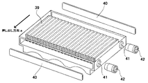
上記のインバータ装置の正面図を図11に、側面図を図12に示す。図11、12において、スイッチングユニット23の下面に冷却ブロック24を配置し、スイッチングユニット23の上面にコンデンサ4を配置している。スイッチングユニット23には接続端子(電源端子)5が一体成型して設けられており(図11)、L字形状の接続導体(ブスライン)15、16を用いてコンデンサ4とスイッチングユニット23が接続されている(図12)。
【0008】
また、インバータ装置に実装されたコンデンサを冷却する構造例として、冷却ブロックの同一載置面上にスイッチングユニットとコンデンサを配置してともに冷却するインバータ装置が開示されている(例えば、特許文献2〜4参照)。
【0009】
【特許文献1】
特開平7−298641号公報(第1−7頁、図3−4)
【特許文献2】
特開平11−346480号公報(第2−4頁、図1)
【特許文献3】
特開2001−86769号公報(第2−3頁、図3)
【特許文献4】
特開2002−16202号公報(第2−6頁、図2−6)
【0010】
【発明が解決しようとする課題】
上記した従来の三相インバータ装置においては、ハイブリッド電気自動車の補助動力としての用途が主であったため、取り扱うインバータ電力は10〜20kWクラスが主流であった。
しかし、シリーズ方式ハイブリッド電気自動車や燃料電池車など、走行用モータのみで駆動する電気自動車においては、取り扱うインバータ電力が40〜100kWと非常に大きくなるため、コンデンサとスイッチングユニット間の接続端子間の接続導体、三相インバータ回路の各端子間の配線を最短にして誘導電圧を抑制しなければならず、また、コンデンサに流れるリプル電流によって生ずる温度上昇を抑制して、コンデンサの寿命低下を抑える必要がある。
今仮に、コンデンサのリプル電流容量を大きくとり、発熱による寿命低下を抑えようとすると、コンデンサが大形化して接続導体が長くなり、配線インダクタンスによる誘導電圧が大きくなってしまうという問題がある。
また、コンデンサを冷却しようとして、スイッチングユニット載置面と同一面上にコンデンサを配置した場合、コンデンサ実装エリアが余分に必要となり冷却ブロックサイズが大きくなってしまうという問題がある。
【0011】
【課題を解決するための手段】
本発明は、上記の課題を解決するものであって、接続端子および接続導体による配線長を極力短くして誘導電圧の低減効果を得るとともに、冷却ブロックの下面を利用しコンデンサを冷却してリプル電流による温度上昇を抑制することで、小形でかつ長寿命のコンデンサを実装するインバータ装置を提供することを目的とする。
【0012】
すなわち、直列接続されたハイサイドスイッチおよびローサイドスイッチにより構成された三組の単相インバータ回路が互いに並列接続されてなる三相インバータ回路で構成され、該回路の(+)、(−)電源端子が(+)ブスラインおよび(−)ブスラインを介して直流電源に接続される半導体モジュールと、(+)充放電端子と(−)充放電端子を有するコンデンサとを冷却ブロックを介して配置したことを特徴とするインバータ装置である。
【0013】
また、上記冷却ブロック載置面と略平行に突出する半導体モジュールの(+)、(−)電源端子とコンデンサの(+)、(−)充放電端子とを各々接続する複数の接続導体とを備え、該接続導体が、コンデンサの(+)、(−)充放電端子からコンデンサ開口面に沿って伸延し、上記半導体モジュール近傍で屈曲し、半導体モジュールの(+)、(−)電源端子に到る側面L字形状の導体板であることを特徴とするインバータ装置である。
【0014】
さらに、上記冷却ブロック載置面と略垂直に突出する半導体モジュールの(+)、(−)電源端子とコンデンサの(+)、(−)充放電端子とを各々接続する複数の接続導体とを備え、上記接続導体が、コンデンサの(+)、(−)充放電端子からコンデンサ開口面に沿って伸延し、半導体モジュールの(+)、(−)電源端子に到る平面状の導体板であって、上記コンデンサの充放電端子と半導体モジュールの電源端子とを略同一方向から固定することを特徴とするインバータ装置である。
【0015】
そして、上記接続導体が、コンデンサの(+)、(−)充放電端子からコンデンサ開口面に沿って伸延し、冷却ブロックまたは半導体モジュール近傍で側面鍵状に屈曲し、半導体モジュールの(+)、(−)電源端子に到る段差状の導体板であって、上記コンデンサの充放電端子と半導体モジュールの電源端子とを略同一方向から固定することを特徴とするインバータ装置である。
【0016】
また、上記コンデンサが、冷却ブロックの載置面に当接する平面を有する偏平型コンデンサであることを特徴とするインバータ装置である。
【0017】
さらに、上記冷却ブロックのコンデンサ側の一部または全部を曲面とし、コンデンサに当接させたことを特徴とするインバータ装置である。
【0018】
そして、上記冷却ブロックの曲面をアルミニウム押し出し材で一体成形して形成したことを特徴とするインバータ装置である。
【0019】
【発明の実施の形態】
半導体モジュール27の(+)電源端子5、(−)電源端子6と略平行となる姿勢で、冷却ブロック24を、半導体モジュール27とコンデンサ33との間に配置し、半導体モジュールの(+)電源端子5、(−)電源端子6と、コンデンサの(+)充放電端子34、(−)充放電端子35とを各々、側面L字形状の接続導体板((+)ブスライン15および(−)ブスライン16)で接続する。
上記構成で、側面L字形状の接続導体板で最短接続することにより、配線インダクタンスによる誘導電圧を抑制し、コンデンサを冷却ブロックに近接配置することで、リプル電流による発熱を抑え、コンデンサの温度上昇を抑制して、インバータ装置の小形化と長寿命化を図ることができる。
【0020】
または、半導体モジュール27、冷却ブロック24、およびコンデンサ33を上記と同様に配置し、半導体モジュール27の側面に沿って屈曲する(+)電源端子5、(−)電源端子6と、コンデンサの(+)充放電端子34、(−)充放電端子35とを各々、平面状または段差状の導体板で、略同一方向からネジ固定する。本構成により、ネジ止めが容易にでき、また、均一な力でネジ固定ができる。
【0021】
そして、上記コンデンサの形状を偏平形とすれば、冷却ブロック24の載置面に当接する平面が形成され、コンデンサと冷却ブロックとの密着性が向上し、コンデンサの冷却が容易となり、リプル電流による温度上昇を抑えることができ、また、半導体モジュールの電源端子と、コンデンサの充放電端子との接続導体配線長が短くなるので、配線インダクタンスによる誘導電圧を低下させることができる。
【0022】
また、上記冷却ブロック24のコンデンサ側をアルミニウム押し出し材で一体成形して曲面を形成し、コンデンサに当接させることで、コンデンサと冷却ブロックとの密着性が向上し、コンデンサの冷却が容易となり、リプル電流による温度上昇を抑えることができる。上記の一体成形は1回の押し出しで可能であるので、冷却ブロックを安価に製作することができる。
【0023】
【実施例】
以下、本発明による実施例について、図面を参照して説明する。
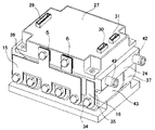
本発明を利用したインバータ装置の斜視図を図2に示し、断面図を図3に示す。図2、3において、半導体モジュール27はアルミニウムからなる冷却ブロック24の載置面28上に熱伝導性グリスを介して配置される。半導体モジュール27の内部には、図1に示すU、V、Wの各相からなる3相インバータ回路および制御ユニット(制御回路)が内蔵され、外部コントローラおよび電流センサに対して接続端子29、30、31を介して接続される。
半導体モジュール27の側面には、(+)電源端子5、(−)電源端子6が上記載置面28に対して略平行となる姿勢で配置され、半導体モジュール27の上面方向からネジ止めにて外部配線と接続できる構造を有している。また、冷却ブロック24の載置面28と相対する面32(以下、冷却ブロックの下面と称する。)には、円筒形コンデンサ33が冷却ブロック24と密着して配置されている。
円筒形コンデンサ33の(+)充放電端子34と(−)充放電端子35は、上記載置面28に対して略平行に突出する姿勢で配置されている。また、半導体モジュール27の(−)電源端子6と円筒形コンデンサ33の(−)充放電端子35はL字形状の(−)ブスライン16で接続され、(+)電源端子5と(+)充放電端子34は、(−)ブスライン16との間に絶縁シート36を挟んで同じくL字形状の(+)ブスライン15で接続される。冷却ブロック24の下面は、円筒形コンデンサ33の曲率半径に合わせて曲面加工がなされており、円筒形コンデンサ33と冷却ブロック下面32との密着性を向上させるとともに、円筒形コンデンサ33上に配置される冷却ブロック24の安定性を向上させている。
また、円筒形コンデンサ33と冷却ブロック24は、コンデンサ底部から冷却ブロック下面32に対して押さえ金具37およびネジ38にて固定している。
【0024】
図4にアルミニウム押し出し材を用いて製作した冷却ブロック24の斜視図を示す。
図4では、アルミ押し出し成型により作成した冷却ブロックケースの内部にアルミニウムにより成型した狭ピッチのコルゲートフィン39を挿入し両側面からアルミニウム板材40で密封しロウ付けしたものを示している。冷却ブロック24には、冷却液循環用のニップル継ぎ手挿入穴41が設けられ、冷却液出入口用ニップル42を圧入することができる。冷却ブロック24の周囲構造は、冷却ブロック空洞部のアルミ押し出し方向aと円筒形コンデンサ33の曲面に密着した構造を同一方向に押し出して成形しているため、1回の押し出し加工でこれらを成形できる。
図4に示す、冷却ブロックの実施例としては三菱マテリアル製の液冷ヒートシンク等を用いることができる。三菱マテリアル製の液冷ヒートシンクの一例として、例えば、縦12.5cm×横23cm×高さ1.6cmの液冷ヒートシンクで約3kWの放熱能力を有するものがある。インバータ装置の出力容量を100kWとし、仮に効率を97%と設定すれば、約3kWの熱損失が発生することになり、これを、冷却ブロックで放熱する必要が生じてくる。100kWクラスのインバータ電力は、ハイブリッド電気自動車の中でも最も大きなクラスの電力を扱うこととなるが、これら大容量のインバータ装置においても冷却ブロックの厚みを1.6cmに抑えることができるため、半導体モジュール27の(+)、(−)電源端子と円筒形コンデンサ33の(+)、(−)充放電端子間を接続する(+)ブスライン15および(−)ブスライン16を、L字形状の導体板とすることで配線長を短く抑えることができ、その結果、配線インダクタンスによる誘導電圧を抑制することができる。
また、円筒形コンデンサ33の放熱向上を目的として、円筒形コンデンサ33と冷却ブロック24の間に高熱伝導性シートを挟み込み、より密着性を向上して円筒形コンデンサ33から冷却ブロック24への熱抵抗を軽減し、コンデンサ内部の温度上昇を抑制させることもできる。
【0025】
図5は、平滑用コンデンサとして、偏平形コンデンサ43を用いた他の実施例の斜視図である。図6は、図5のうち偏平形コンデンサ43と冷却ブロック24の密着構造を示したものである。
図6に示す偏平形コンデンサ43はその厚さ方向が冷却ブロック24の載置面28に対して略垂直となる姿勢で、冷却ブロック24に近接配置させることで、冷却ブロック24との密着性がより向上する。従って、偏平形コンデンサ43を冷却するための冷却ブロック24の下面構造として、偏平型コンデンサ43の角部のRに合わせた嵌合部44をアルミ押し出し成形で設けることも可能であり、また、嵌合部44をなくして、冷却ブロック下面32を完全に平面にすることも可能である。
また、偏平形コンデンサ43を使用することで、その厚さ方向が幅方向よりも短くなることから、半導体モジュール27の(+)、(−)電源端子と偏平形コンデンサ43の(+)、(−)充放電端子間の接続導体の長さを、図2、3の円筒型コンデンサを使用した実施例よりもさらに短く抑えることができ、その結果、配線インダクタンスはさらに低減され、誘導電圧をより低下させたインバータ装置を提供することができる。
【0026】
図7、8は本発明によるインバータ装置の他の実施例であり、半導体モジュール27、冷却ブロック24、および円筒形コンデンサ33を図2、3と同様に配置し、半導体モジュール27の側面に沿って屈曲する(+)電源端子5、(−)電源端子6と、円筒形コンデンサ33の(+)充放電端子34、(−)充放電端子35とを各々、平面状の導体板で、略同一方向からネジ固定したものである(図7:斜視図、図8:断面図)。
半導体モジュール27の電源端子が側面に沿って屈曲する形状であり、該端子と、コンデンサの充放電端子とを、平面状の導体板で、略同一方向からネジ固定した点が、図2、3と相違するが、構成は同様であり、説明は省略する。図7、8のように構成することで、ネジ止めが同一方向から容易にでき、また、均一な力でネジ固定ができる。
【0027】
図9は、本発明によるインバータ装置の他の実施例(斜視図)であり、平滑用コンデンサとして偏平形コンデンサ43を用い、半導体モジュール27の側面に沿って屈曲する(+)電源端子5、(−)電源端子6と、偏平形コンデンサ43の(+)充放電端子34、(−)充放電端子35とを各々、平面状の導体板で、略同一方向からネジ固定したもので、図7の場合と同様、ネジ止めが同一方向から容易にでき、また、均一な力でネジ固定ができる。その他の構成は図7と同様であり、説明は省略する。
コンデンサの形状を偏平形とすることで、図2の場合と同様、冷却ブロック24の載置面に当接する平面が形成され、コンデンサと冷却ブロックとの密着性が向上し、コンデンサの冷却が容易となり、リプル電流による温度上昇を抑えることができ、また、半導体モジュールの電源端子と、コンデンサの充放電端子との接続導体配線長が短くなるので、配線インダクタンスによる誘導電圧を低下させることができる
【0028】
図10は、本発明によるインバータ装置の他の実施例(断面図)であり、半導体モジュール27、冷却ブロック24、および円筒形コンデンサ33を図2、3と同様に配置し、半導体モジュール27の(+)電源端子5、(−)電源端子6と、円筒形コンデンサ33の(+)充放電端子34、(−)充放電端子35とを各々、段差状の導体板で、略同一方向からネジ固定したものである。ここで、段差状の導体板を用いるのは、上記部品の配置が予め決められており、動かせない場合を考慮したものである。
半導体モジュール27の電源端子が側面に沿って屈曲する形状であり、該端子と、コンデンサの充放電端子とを、段差状の導体板で、略同一方向からネジ固定した点が、図2、3と相違するが、構成は同様であり、説明は省略する。図10のように構成することで、ネジ止めが同一方向から容易にでき、また、均一な力でネジ固定ができる。その他の構成は図8と同様であり、説明は省略する。
【0029】
【発明の効果】
以上説明したように、半導体モジュールの電源端子と略平行となる姿勢で、冷却ブロックを、半導体モジュールとコンデンサとの間に配置し、半導体モジュールの電源端子と、コンデンサの充放電端子とを各々、側面L字形状の接続導体板で接続しているので、側面L字形状の接続導体板で最短接続することになり、配線インダクタンスによる誘導電圧を低下させることができ、コンデンサを冷却ブロックに近接配置することで、リプル電流による発熱を冷却ブロック側に放熱し、コンデンサの温度上昇を抑制して、インバータ装置の小型化と長寿命化を計ることができる。
または、半導体モジュールの電源端子と、コンデンサの充放電端子とを各々、平面状または段差状の導体板で、略同一方向からネジ固定することで、ネジ止めが容易にでき、また、均一な力でネジ固定ができる。
さらに、上記コンデンサの形状を偏平形とすることで、冷却ブロックの載置面に当接する平面が形成され、コンデンサと冷却ブロックとの密着性が向上し、コンデンサの冷却が容易となり、リプル電流による温度上昇を抑えることができ、また、半導体モジュールの電源端子と、コンデンサの充放電端子との接続導体配線長が短くなるので、配線インダクタンスによる誘導電圧を低下させることができる。
そして、冷却ブロックのコンデンサ側をアルミニウム押し出し材で一体成形して曲面を形成し、コンデンサに当接させることで、コンデンサと冷却ブロックとの密着性が向上し、コンデンサの冷却が容易となり、リプル電流による温度上昇を抑えることができる。
以上に示すとおり、本構造によるインバータ装置により、配線インダクタンスによる誘導電圧を抑制しつつコンデンサの小形化と長寿命化を達成することができる。
【図面の簡単な説明】
【図1】本発明の実施例によるインバータ装置の回路図である。
【図2】本発明の実施例によるインバータ装置の斜視図である。
【図3】図2のインバータ装置の断面図である。
【図4】図2に示すインバータ装置の冷却ブロックの構造図である。
【図5】本発明の他の実施例によるインバータ装置の斜視図である。
【図6】図5に示すインバータ装置の冷却ブロックと偏平形コンデンサの取付構造の説明図である。
【図7】本発明の他の実施例によるインバータ装置の斜視図である。
【図8】図7のインバータ装置の断面図である。
【図9】本発明の他の実施例によるインバータ装置の斜視図である。
【図10】本発明の他の実施例によるインバータ装置の断面図である。
【図11】従来のインバータ装置の正面図である。
【図12】従来のインバータ装置の側面図である。
【符号の説明】
1 直流電源(主バッテリ)
2 インバータ装置
3 走行モータ
4 平滑コンデンサ
5 (+)電源端子
6 (−)電源端子
7 U相インバータ回路(スイッチ回路)
8 V相インバータ回路(スイッチ回路)
9 W相インバータ回路(スイッチ回路)
10 制御ユニット
11a、11b 電流センサ
12a、12b 外部コントローラ信号
13 絶縁被覆ケーブル
14 絶縁被覆ケーブル
15 (+)ブスライン(接続導体)
16 (−)ブスライン(接続導体)
17 U相ブスライン
18 V相ブスライン
19 W相ブスライン
20 絶縁被覆ケーブル
21 絶縁被覆ケーブル
22 絶縁被覆ケーブル
23 スイッチングユニット
24 冷却ブロック
25 コンデンサ固定支持台
26 半導体モジュール
27 冷却ブロック載置面
28 外部コントローラ接続端子
29 電流センサ接続端子
30 電流センサ接続端子
31 冷却ブロック下面
32 円筒形コンデンサ
33 (+)充放電端子
34 (−)充放電端子
35 絶縁シート
36 押さえ金具
37 ネジ
38 コルゲートフィン
39 アルミニウム板材
40 ニップル継ぎ手挿入穴
41 ニップル
42 偏平形コンデンサ
43 冷却ブロック嵌合部[0001]
TECHNICAL FIELD OF THE INVENTION
The present invention relates to a three-phase inverter device that controls a traveling motor or the like of an electric vehicle, and particularly to a three-phase inverter device that drives and controls a traveling motor of a hybrid electric vehicle.
[0002]
[Prior art]
BACKGROUND ART Conventionally, a three-phase inverter device can recover rotational energy of a load as electric power to a DC power source side by a regenerative operation at the time of braking, and thus is widely used for driving motor drive control of an electric vehicle. A conventional three-phase inverter device used for controlling a traveling motor of a hybrid electric vehicle will be described with reference to FIG.
[0003]
In FIG. 1, a DC power supply 1 is a main battery in which a plurality of nickel-metal hydride batteries or lithium-ion batteries are connected in series, and is connected to a three-phase inverter via insulation coated cables 13 and 14 and (+) bus lines 15 and (−) bus lines 16. Connected to device 2. The smoothing capacitor 4 connected to the input stage of the three-phase inverter device 2 stabilizes the bus line voltage by absorbing the ripple current when driving the inverter.
[0004]
In the three-phase inverter device 2, 7a to 9a and 7b to 9b are IGBTs, and the high-side switch 7a and the low-side switch 7b connected in series constitute a U-phase switch circuit 7, and the high-side switches connected in series. 8a and the low-side switch 8b constitute a V-phase switch circuit 8, and the high-side switch 9a and the low-side switch 9b connected in series constitute a W-phase switch circuit 9.
A U-phase output terminal 7e, which is a connection point between the high-side switch 7a and the low-side switch 7b, a V-phase output terminal 8e, which is a connection point between the high-side switch 8a and the low-side switch 8b, and a high-side switch 9a and the low-side switch A W-phase output terminal 9e, which is a connection point with 9b, is individually connected to each phase terminal of the traveling motor through each U-phase bus line 17, V-phase bus line 18, W-phase bus line 19, and insulation-coated cables 20, 21, and 22. Then, the U, V, and W phase inverter circuits (switch circuits) are alternately turned on / off by using a control unit 10 described later to convert the DC power supplied from the DC power supply 1 into three-phase AC power. Power is supplied to the traveling motor 3.
The flywheel diodes 7c to 9c and 7d to 9d are individually connected in parallel with the IGBTs 7a to 9a and 7b to 9b to supply a return current to the traveling motor 3 that is an inductive load.
[0005]
The control unit 10 built in the three-phase inverter device 2 controls each of the IGBTs 7a to 9a based on a signal related to a phase current supplied to the traveling motor 3 detected by the current sensors 11a and 11b and a command signal 12a from an external controller. , 7b-9b can be intermittently controlled to generate a stable three-phase AC voltage.
[0006]
As a structural example of the above three-phase inverter device, a high-side switch and a low-side switch are constituted by a single-phase inverter circuit connected in series, and the (+) and (-) power supply terminals are (+) bus line and (-) bus line. Device comprising a predetermined number of switching units connected to a DC power supply through a capacitor, the (+) and (-) charging / discharging terminals of the capacitor are connected to the (+) and (-) power supply terminals of each of the switching units, respectively. There is disclosed an inverter device that is connected by a letter-shaped conductor plate to suppress an induced voltage due to wiring inductance (for example, see Patent Document 1).
[0007]
FIG. 11 is a front view and FIG. 12 is a side view of the inverter device. 11 and 12, the cooling block 24 is disposed on the lower surface of the switching unit 23, and the capacitor 4 is disposed on the upper surface of the switching unit 23. The switching unit 23 is provided with a connection terminal (power supply terminal) 5 integrally formed therewith (FIG. 11), and the capacitor 4 and the switching unit 23 are connected using L-shaped connection conductors (bus lines) 15 and 16. (FIG. 12).
[0008]
As an example of a structure for cooling a capacitor mounted on an inverter device, an inverter device that disposes a switching unit and a capacitor on the same mounting surface of a cooling block and cools both is disclosed (for example, Patent Documents 2 to 4). 4).
[0009]
[Patent Document 1]
JP-A-7-2988641 (pages 1-7, FIG. 3-4)
[Patent Document 2]
JP-A-11-346480 (pages 2-4, FIG. 1)
[Patent Document 3]
JP 2001-86669 A (page 2-3, FIG. 3)
[Patent Document 4]
JP-A-2002-16202 (page 2-6, FIG. 2-6)
[0010]
[Problems to be solved by the invention]
In the above-mentioned conventional three-phase inverter device, since it is mainly used as an auxiliary power of a hybrid electric vehicle, the inverter power to be handled is mainly in a class of 10 to 20 kW.
However, in the case of an electric vehicle driven only by a driving motor, such as a series hybrid electric vehicle or a fuel cell vehicle, the inverter power to be handled is as large as 40 to 100 kW. It is necessary to suppress the induced voltage by minimizing the wiring between the conductors and the terminals of the three-phase inverter circuit, and to suppress the temperature rise caused by the ripple current flowing through the capacitor, and to suppress the shortening of the life of the capacitor. is there.
If the ripple current capacity of the capacitor is increased to suppress the reduction in life due to heat generation, there is a problem that the capacitor becomes large, the connection conductor becomes long, and the induced voltage due to the wiring inductance increases.
Further, when the capacitors are arranged on the same surface as the switching unit mounting surface in an attempt to cool the capacitors, there is a problem that an extra capacitor mounting area is required and the cooling block size becomes large.
[0011]
[Means for Solving the Problems]
The present invention solves the above-described problems, and achieves an effect of reducing an induced voltage by shortening a wiring length of a connection terminal and a connection conductor as much as possible. It is an object of the present invention to provide an inverter device which mounts a small-sized and long-life capacitor by suppressing a temperature rise due to a current.
[0012]
That is, a three-phase inverter circuit is formed by connecting three sets of single-phase inverter circuits each composed of a high-side switch and a low-side switch connected in series, and a (+) and (-) power supply terminals of the circuit. Is that a semiconductor module connected to a DC power supply via a (+) bus line and a (-) bus line and a capacitor having a (+) charge / discharge terminal and a (-) charge / discharge terminal are arranged via a cooling block. This is a characteristic inverter device.
[0013]
Also, a plurality of connection conductors respectively connecting the (+) and (-) power supply terminals of the semiconductor module and the (+) and (-) charge / discharge terminals of the capacitor protruding substantially parallel to the cooling block mounting surface. The connection conductor extends from the (+) and (-) charge / discharge terminals of the capacitor along the opening surface of the capacitor, bends near the semiconductor module, and connects to the (+) and (-) power supply terminals of the semiconductor module. An inverter device characterized by a conductor plate having an L-shaped side surface.
[0014]
Further, a plurality of connection conductors respectively connecting the (+) and (-) power supply terminals of the semiconductor module and the (+) and (-) charge / discharge terminals of the capacitor protruding substantially perpendicular to the cooling block mounting surface. The connection conductor is a planar conductor plate extending from the (+) and (-) charge / discharge terminals of the capacitor along the opening surface of the capacitor and reaching the (+) and (-) power terminals of the semiconductor module. The charging / discharging terminal of the capacitor and the power supply terminal of the semiconductor module are fixed from substantially the same direction.
[0015]
Then, the connection conductor extends from the (+), (-) charge / discharge terminal of the capacitor along the opening surface of the capacitor, bends in the shape of a side key near the cooling block or the semiconductor module, and (+), (-) A stepped conductor plate reaching a power supply terminal, wherein the charge / discharge terminal of the capacitor and the power supply terminal of the semiconductor module are fixed from substantially the same direction.
[0016]
Further, the inverter device is characterized in that the capacitor is a flat type capacitor having a flat surface in contact with the mounting surface of the cooling block.
[0017]
Further, the inverter device is characterized in that a part or the whole of the cooling block on the condenser side has a curved surface and is brought into contact with the condenser.
[0018]
The curved surface of the cooling block is integrally formed with an extruded aluminum material to form an inverter device.
[0019]
BEST MODE FOR CARRYING OUT THE INVENTION
The cooling block 24 is disposed between the semiconductor module 27 and the capacitor 33 so as to be substantially parallel to the (+) power supply terminal 5 and the (−) power supply terminal 6 of the semiconductor module 27, and the (+) power supply The terminal 5, the (-) power supply terminal 6, and the (+) charging / discharging terminal 34 and (-) charging / discharging terminal 35 of the capacitor are respectively connected to the L-shaped side connection conductor plate ((+) bus line 15 and (-)). Bus line 16).
In the above configuration, the shortest connection with the L-shaped side connection conductor plate suppresses the induced voltage due to the wiring inductance, and disposes the capacitor close to the cooling block, thereby suppressing heat generation due to ripple current and increasing the temperature of the capacitor. , And downsizing and long life of the inverter device can be achieved.
[0020]
Alternatively, the semiconductor module 27, the cooling block 24, and the capacitor 33 are arranged in the same manner as described above, and the (+) power supply terminal 5, the (-) power supply terminal 6 that bends along the side surface of the semiconductor module 27, and the (+) of the capacitor. ) The charging / discharging terminal 34 and the (-) charging / discharging terminal 35 are each fixed by screws from substantially the same direction using a planar or stepped conductor plate. With this configuration, the screws can be easily fixed, and the screws can be fixed with a uniform force.
[0021]
If the shape of the capacitor is flat, a flat surface is formed in contact with the mounting surface of the cooling block 24, the adhesion between the capacitor and the cooling block is improved, the cooling of the capacitor is facilitated, and the ripple current is reduced. The temperature rise can be suppressed, and the length of the connecting conductor wiring between the power supply terminal of the semiconductor module and the charge / discharge terminal of the capacitor is shortened, so that the induced voltage due to the wiring inductance can be reduced.
[0022]
In addition, the capacitor side of the cooling block 24 is integrally molded with an extruded aluminum material to form a curved surface, and by contacting the capacitor, the adhesion between the capacitor and the cooling block is improved, and cooling of the capacitor is facilitated. Temperature rise due to ripple current can be suppressed. Since the above-described integral molding can be performed by one extrusion, the cooling block can be manufactured at low cost.
[0023]
【Example】
Hereinafter, embodiments of the present invention will be described with reference to the drawings.
FIG. 2 is a perspective view of an inverter device using the present invention, and FIG. 3 is a cross-sectional view thereof. 2 and 3, the semiconductor module 27 is disposed on the mounting surface 28 of the cooling block 24 made of aluminum via thermally conductive grease. Inside the semiconductor module 27, a three-phase inverter circuit composed of U, V, and W phases and a control unit (control circuit) shown in FIG. 1 are incorporated, and connection terminals 29, 30 for an external controller and a current sensor are provided. , 31 are connected.
On the side surface of the semiconductor module 27, the (+) power terminal 5 and the (-) power terminal 6 are arranged in a posture substantially parallel to the mounting surface 28, and are screwed from the upper surface direction of the semiconductor module 27. It has a structure that can be connected to external wiring. On a surface 32 of the cooling block 24 facing the mounting surface 28 (hereinafter, referred to as a lower surface of the cooling block), a cylindrical condenser 33 is disposed in close contact with the cooling block 24.
The (+) charging / discharging terminal 34 and the (−) charging / discharging terminal 35 of the cylindrical capacitor 33 are arranged in a posture protruding substantially parallel to the mounting surface 28. The (−) power supply terminal 6 of the semiconductor module 27 and the (−) charge / discharge terminal 35 of the cylindrical capacitor 33 are connected by an L-shaped (−) bus line 16, and the (+) power supply terminal 5 and the (+) charge The discharge terminal 34 is connected to the (-) bus line 16 via the (+) bus line 15 having the same L-shape with the insulating sheet 36 interposed therebetween. The lower surface of the cooling block 24 is subjected to a curved surface processing in accordance with the radius of curvature of the cylindrical capacitor 33 to improve the adhesion between the cylindrical capacitor 33 and the lower surface 32 of the cooling block, and is disposed on the cylindrical capacitor 33. The stability of the cooling block 24 is improved.
The cylindrical condenser 33 and the cooling block 24 are fixed from the bottom of the condenser to the lower surface 32 of the cooling block by holding metal members 37 and screws 38.
[0024]
FIG. 4 is a perspective view of a cooling block 24 manufactured using an extruded aluminum material.
FIG. 4 shows a case in which corrugated fins 39 of narrow pitch made of aluminum are inserted into a cooling block case made by aluminum extrusion molding, sealed with aluminum plate materials 40 from both sides, and brazed. The cooling block 24 is provided with a nipple joint insertion hole 41 for circulating a coolant, and a nipple 42 for a coolant inlet / outlet can be press-fitted therein. The surrounding structure of the cooling block 24 is formed by extruding the structure in close contact with the curved surface of the cylindrical capacitor 33 in the same direction as the aluminum extruding direction a of the cooling block cavity in the same direction. .
As an example of the cooling block shown in FIG. 4, a liquid-cooled heat sink made by Mitsubishi Materials or the like can be used. As an example of a liquid cooling heat sink manufactured by Mitsubishi Materials, for example, there is a liquid cooling heat sink having a length of 12.5 cm, a width of 23 cm, and a height of 1.6 cm and having a heat radiation capacity of about 3 kW. If the output capacity of the inverter device is set to 100 kW and the efficiency is set to 97%, a heat loss of about 3 kW occurs, and it becomes necessary to radiate the heat loss by the cooling block. The inverter power of the 100 kW class handles the largest class of electric power among hybrid electric vehicles. However, even in these large-capacity inverter devices, the thickness of the cooling block can be suppressed to 1.6 cm. The (+) bus line 15 and the (-) bus line 16 for connecting the (+) and (-) power supply terminals of the cylindrical capacitor 33 with the (+) and (-) charge / discharge terminals of the cylindrical capacitor 33 are connected to an L-shaped conductor plate. By doing so, the wiring length can be kept short, and as a result, the induced voltage due to the wiring inductance can be suppressed.
Further, for the purpose of improving the heat radiation of the cylindrical capacitor 33, a high heat conductive sheet is interposed between the cylindrical capacitor 33 and the cooling block 24 to further improve the adhesion and to reduce the heat resistance from the cylindrical capacitor 33 to the cooling block 24. And the temperature rise inside the capacitor can be suppressed.
[0025]
FIG. 5 is a perspective view of another embodiment using a flat capacitor 43 as a smoothing capacitor. FIG. 6 shows the close contact structure between the flat condenser 43 and the cooling block 24 in FIG.
The flat type capacitor 43 shown in FIG. 6 is disposed close to the cooling block 24 in a position where its thickness direction is substantially perpendicular to the mounting surface 28 of the cooling block 24, so that the close contact with the cooling block 24 is improved. Better. Therefore, as a lower surface structure of the cooling block 24 for cooling the flat capacitor 43, a fitting portion 44 corresponding to the R of the corner of the flat capacitor 43 can be provided by aluminum extrusion molding. It is also possible to eliminate the joint portion 44 and make the cooling block lower surface 32 completely flat.
In addition, since the thickness direction becomes shorter than the width direction by using the flat capacitor 43, the (+) and (-) power supply terminals of the semiconductor module 27 and the (+) and ( -) The length of the connecting conductor between the charging and discharging terminals can be further reduced as compared with the embodiment using the cylindrical capacitor shown in FIGS. 2 and 3, so that the wiring inductance is further reduced and the induced voltage is further reduced. A lowered inverter device can be provided.
[0026]
7 and 8 show another embodiment of the inverter device according to the present invention, in which the semiconductor module 27, the cooling block 24, and the cylindrical capacitor 33 are arranged in the same manner as in FIGS. The (+) power supply terminal 5 and the (-) power supply terminal 6 that bend and the (+) charge / discharge terminal 34 and (−) charge / discharge terminal 35 of the cylindrical capacitor 33 are substantially the same as a planar conductor plate. It is screw-fixed from the direction (FIG. 7: perspective view, FIG. 8: sectional view).
The power supply terminal of the semiconductor module 27 has a shape that bends along the side surface, and the terminal and the charge / discharge terminal of the capacitor are fixed by screws in substantially the same direction using a planar conductor plate. However, the configuration is the same, and the description is omitted. 7 and 8, screws can be easily fixed from the same direction, and screws can be fixed with a uniform force.
[0027]
FIG. 9 shows another embodiment (perspective view) of an inverter device according to the present invention, in which a flat capacitor 43 is used as a smoothing capacitor, and a (+) power supply terminal 5, which is bent along the side surface of the semiconductor module 27, -) The power supply terminal 6 and the (+) charge / discharge terminals 34 and (-) charge / discharge terminals 35 of the flat type capacitor 43 are each fixed by screws from substantially the same direction with a planar conductor plate. As in the case of (1), screwing can be easily performed from the same direction, and the screw can be fixed with a uniform force. Other configurations are the same as those in FIG. 7, and the description is omitted.
By making the shape of the capacitor a flat shape, as in the case of FIG. 2, a flat surface is formed which is in contact with the mounting surface of the cooling block 24, the adhesion between the capacitor and the cooling block is improved, and the cooling of the capacitor is facilitated. As a result, the rise in temperature due to ripple current can be suppressed, and the length of the connection conductor wiring between the power supply terminal of the semiconductor module and the charge / discharge terminal of the capacitor becomes shorter, so that the induced voltage due to the wiring inductance can be reduced. 0028
FIG. 10 is another embodiment (cross-sectional view) of the inverter device according to the present invention, in which the semiconductor module 27, the cooling block 24, and the cylindrical capacitor 33 are arranged in the same manner as in FIGS. The (+) power supply terminal 5, (-) power supply terminal 6, and the (+) charge / discharge terminal 34, (-) charge / discharge terminal 35 of the cylindrical capacitor 33 are each a stepped conductor plate and screwed from substantially the same direction. It is fixed. Here, the stepped conductor plate is used in consideration of a case where the arrangement of the components is predetermined and the component cannot be moved.
The power supply terminal of the semiconductor module 27 has a shape that bends along the side surface, and the terminal and the charge / discharge terminal of the capacitor are screw-fixed from substantially the same direction with a stepped conductor plate as shown in FIGS. However, the configuration is the same, and the description is omitted. With the configuration as shown in FIG. 10, screwing can be easily performed from the same direction, and the screw can be fixed with a uniform force. Other configurations are the same as those in FIG. 8, and the description is omitted.
[0029]
【The invention's effect】
As described above, the cooling block is disposed between the semiconductor module and the capacitor in a posture substantially parallel to the power supply terminal of the semiconductor module, and the power supply terminal of the semiconductor module and the charge / discharge terminal of the capacitor are respectively provided. Since the connection is made with the side L-shaped connection conductor plate, the connection is made as short as possible with the side L-shaped connection conductor plate, the induced voltage due to the wiring inductance can be reduced, and the capacitor is arranged close to the cooling block. By doing so, the heat generated by the ripple current is radiated to the cooling block side, the temperature rise of the capacitor is suppressed, and the size and the life of the inverter device can be reduced.
Alternatively, the power supply terminal of the semiconductor module and the charge / discharge terminal of the capacitor are each fixed with screws from substantially the same direction using a planar or stepped conductor plate, so that the screws can be easily screwed and uniform force can be obtained. Can be fixed with screws.
Further, by making the shape of the capacitor flat, a flat surface is formed in contact with the mounting surface of the cooling block, the adhesion between the capacitor and the cooling block is improved, the cooling of the capacitor is facilitated, and the ripple current is reduced. The temperature rise can be suppressed, and the length of the connecting conductor wiring between the power supply terminal of the semiconductor module and the charge / discharge terminal of the capacitor is shortened, so that the induced voltage due to the wiring inductance can be reduced.
Then, the capacitor side of the cooling block is integrally molded with extruded aluminum to form a curved surface, and by making contact with the capacitor, the adhesion between the capacitor and the cooling block is improved, cooling of the capacitor is facilitated, and ripple current is reduced. Temperature rise due to the above can be suppressed.
As described above, with the inverter device having the present structure, it is possible to reduce the size and increase the life of the capacitor while suppressing the induced voltage due to the wiring inductance.
[Brief description of the drawings]
FIG. 1 is a circuit diagram of an inverter device according to an embodiment of the present invention.
FIG. 2 is a perspective view of an inverter device according to an embodiment of the present invention.
FIG. 3 is a sectional view of the inverter device of FIG. 2;
FIG. 4 is a structural diagram of a cooling block of the inverter device shown in FIG. 2;
FIG. 5 is a perspective view of an inverter device according to another embodiment of the present invention.
6 is an explanatory diagram of a mounting structure of a cooling block and a flat capacitor of the inverter device shown in FIG.
FIG. 7 is a perspective view of an inverter device according to another embodiment of the present invention.
FIG. 8 is a sectional view of the inverter device of FIG. 7;
FIG. 9 is a perspective view of an inverter device according to another embodiment of the present invention.
FIG. 10 is a sectional view of an inverter device according to another embodiment of the present invention.
FIG. 11 is a front view of a conventional inverter device.
FIG. 12 is a side view of a conventional inverter device.
[Explanation of symbols]
1 DC power supply (main battery)
2 Inverter device 3 Traveling motor 4 Smoothing capacitor 5 (+) Power terminal 6 (-) Power terminal 7 U-phase inverter circuit (switch circuit)
8 V phase inverter circuit (switch circuit)
9 W-phase inverter circuit (switch circuit)
Reference Signs List 10 Control units 11a, 11b Current sensors 12a, 12b External controller signal 13 Insulated cable 14 Insulated cable 15 (+) bus line (connection conductor)
16 (-) bus line (connection conductor)
17 U-phase bus line 18 V-phase bus line 19 W-phase bus line 20 Insulated cable 21 Insulated cable 22 Insulated cable 23 Switching unit 24 Cooling block 25 Capacitor fixed support 26 Semiconductor module 27 Cooling block mounting surface 28 External controller connection terminal 29 Current sensor connection terminal 30 Current sensor connection terminal 31 Cooling block lower surface 32 Cylindrical capacitor 33 (+) charge / discharge terminal 34 (−) charge / discharge terminal 35 Insulating sheet 36 Pressing fitting 37 Screw 38 Corrugated fin 39 Aluminum plate 40 Nipple joint insertion hole 41 Nipple 42 Flat type condenser 43 Cooling block fitting part