JP2004247716A - Method for manufacturing laminated body - Google Patents
Method for manufacturing laminated body Download PDFInfo
- Publication number
- JP2004247716A JP2004247716A JP2004011131A JP2004011131A JP2004247716A JP 2004247716 A JP2004247716 A JP 2004247716A JP 2004011131 A JP2004011131 A JP 2004011131A JP 2004011131 A JP2004011131 A JP 2004011131A JP 2004247716 A JP2004247716 A JP 2004247716A
- Authority
- JP
- Japan
- Prior art keywords
- organic semiconductor
- thin film
- substrate
- film
- light
- Prior art date
- Legal status (The legal status is an assumption and is not a legal conclusion. Google has not performed a legal analysis and makes no representation as to the accuracy of the status listed.)
- Pending
Links
Images


Abstract
Description
本発明は、スイッチングや増幅素子として有用な電子デバイスに用いることができる有機半導体膜を有する積層体の製造方法に関するものである。 The present invention relates to a method for manufacturing a laminate having an organic semiconductor film that can be used for an electronic device useful as a switching or amplification element.
電界効果トランジスタ、ダイオード、光ダイオードおよび太陽電池などの電子デバイスには、無機半導体材料からなる素子を用いるのが一般的である。 BACKGROUND ART For electronic devices such as field effect transistors, diodes, photodiodes, and solar cells, it is common to use elements made of inorganic semiconductor materials.
例えば、電界効果トランジスタは、バイポーラトランジスタと並んで重要なスイッチ、増幅素子として広く利用されているが、これまではシリコンを用いた素子が広く用いられている。電界効果トランジスタは、半導体材料にソースとドレイン電極、絶縁体層を介してゲート電極を設けた構造を有しており、基本的には、p型あるいはn型の一方のキャリアが電荷を輸送し、ユニポーラ素子の代表的なものである。 For example, a field effect transistor is widely used as an important switch and amplifying element along with a bipolar transistor, but an element using silicon has been widely used so far. A field-effect transistor has a structure in which a semiconductor material is provided with a source and drain electrodes and a gate electrode with an insulator layer interposed therebetween. Basically, one of p-type and n-type carriers transports charges. , A typical unipolar element.
近年、これら電子デバイスの半導体層として、有機半導体材料を用いる試みがなされている。導電性高分子、共役高分子を利用した例(特許文献1)、低分子化合物を利用した例(特許文献2)が報告されている。 In recent years, attempts have been made to use organic semiconductor materials as semiconductor layers of these electronic devices. An example using a conductive polymer and a conjugated polymer (Patent Document 1) and an example using a low molecular compound (Patent Document 2) have been reported.
有機半導体材料を用いた有機電子デバイスは、無機半導体材料を用いる場合に比べて低温プロセスで製造できるため、プラスチック基板やフィルムを用いることができ、軽量で壊れにくい素子を作製することができる。また、溶液の塗布や印刷法を用いた素子作製が可能なものもあり、大面積の素子を低コストで製造することが可能である。さらに、材料のバリエーションが豊富であり、分子構造を変化させることにより容易に材料特性を根本的に変化させることが可能であるため、異なる機能を組み合わせることで、無機半導体では不可能な機能、素子を実現することも可能であるといった利点を有するものである。 Since an organic electronic device using an organic semiconductor material can be manufactured by a low-temperature process as compared with a case using an inorganic semiconductor material, a plastic substrate or a film can be used, and a light-weight and hard-to-break element can be manufactured. Some devices can be manufactured by applying a solution or using a printing method, and thus a large-area device can be manufactured at low cost. Furthermore, since there are a wide variety of materials and it is possible to fundamentally change the material properties easily by changing the molecular structure, functions and elements that are impossible with inorganic semiconductors by combining different functions Can also be realized.
一方、有機半導体材料はπ電子共役分子がほとんどであるが、その剛直な構造のため有機溶媒に対する溶解度が極端に低いものが多い。そのため溶解度の低い半導体膜の形成には蒸着法等の真空製膜が用いられることが多く、これでは低コストで製造可能という有機物のメリットを減じることになる。 On the other hand, most organic semiconductor materials have π-electron conjugated molecules, but due to their rigid structure, many have extremely low solubility in organic solvents. For this reason, a vacuum film formation method such as a vapor deposition method is often used for forming a semiconductor film having low solubility, which reduces the merit of an organic material that can be manufactured at low cost.
低溶解性の有機半導体膜を塗布で作製する方法の一つに、基板上に可溶性の前駆体の膜を塗布で作製した後に最終的な半導体に変換する方法が知られており、ポリチエニレンビニレンの例(非特許文献1)、ペンタセンの例(非特許文献2および非特許文献3)等が報告されている。しかしながら、前駆体の塗布膜を半導体に変換するためには、いずれも200℃程度の加熱が必要であるため、この加熱温度に耐える樹脂基板材料はポリイミド等の特殊なものに限られてしまう。
As one of the methods for producing a low-solubility organic semiconductor film by coating, a method is known in which a film of a soluble precursor is formed on a substrate by coating and then converted into a final semiconductor. Examples of vinylene (Non-Patent Document 1) and examples of pentacene (Non-Patent
また、一方で、有機半導体膜を加熱することにより半導体の特性が向上することが知られている(特許文献3)。このように加熱により有機半導体の特性が向上する原因としては、結晶の成長、欠陥の低減、不純物の除去、電極−半導体等の接合状態の改良等が考えられ、一般の有機半導体に適用可能である。しかしながら、この場合も、加熱温度は基板等の耐熱温度以下に制限されるため、特に基板に樹脂基板を用いる際には十分な加熱処理ができないことが多い。 On the other hand, it is known that the characteristics of a semiconductor are improved by heating an organic semiconductor film (Patent Document 3). The cause of the improvement of the characteristics of the organic semiconductor by heating in this way is considered to be crystal growth, reduction of defects, removal of impurities, improvement of the bonding state of the electrode-semiconductor, and the like, which is applicable to general organic semiconductors. is there. However, also in this case, since the heating temperature is limited to the heat-resistant temperature of the substrate or the like, a sufficient heat treatment cannot be often performed particularly when a resin substrate is used as the substrate.
本発明は、基板上に有機半導体膜を形成する際に、基板の耐熱温度に制限されることなく、有機半導体からなる薄膜の特性改良または有機半導体の前駆体からなる薄膜の有機半導体への変換を可能にし、基板上に良好な有機半導体膜を形成することのできる有機半導体膜を含む積層体の製造方法を提供することを主目的とする。 The present invention is intended to improve the characteristics of a thin film composed of an organic semiconductor or to convert a thin film composed of a precursor of an organic semiconductor into an organic semiconductor, without being limited by the heat-resistant temperature of the substrate, when forming an organic semiconductor film on a substrate. It is an object of the present invention to provide a method for manufacturing a laminate including an organic semiconductor film, which enables formation of a favorable organic semiconductor film on a substrate.
本発明者らは、上記実情に鑑み鋭意検討した結果、有機半導体またはその前駆体からなる薄膜を形成した後、光照射を用いることにより、加熱による基板等の周辺部へのダメージを伴うことなく良好な有機半導体膜を形成できることを見出して本発明に到達した。 The present inventors have conducted intensive studies in view of the above circumstances, and as a result, after forming a thin film made of an organic semiconductor or a precursor thereof, by using light irradiation, without causing damage to a peripheral portion such as a substrate due to heating. The present inventors have found that a good organic semiconductor film can be formed, and have reached the present invention.
すなわち、本発明においては、請求項1に記載するように、基板上に少なくとも有機半導体またはその前駆体からなる薄膜を形成した後、活性エネルギー線を照射する工程を含むことを特徴とする積層体の製造方法を提供する。
That is, according to the present invention, as described in
本発明は、基板上に少なくとも有機半導体またはその前駆体からなる薄膜を形成した後、活性エネルギー線を照射する工程を行うものであるので、例えば有機半導体の前駆体を塗布法により塗布して薄膜形成を行い、その後活性エネルギー線の照射を行うことにより基材上に有機半導体膜が形成された積層体を低コストで得ることができる。また、予め形成された有機半導体薄膜に対して活性エネルギー線を照射することにより、最終的に得られる有機半導体膜の特性を向上させることができる等の利点を有するものである。 Since the present invention forms a thin film composed of at least an organic semiconductor or a precursor thereof on a substrate, and then performs a step of irradiating active energy rays, for example, applying a precursor of an organic semiconductor by a coating method to form a thin film By forming and then irradiating with active energy rays, a laminate in which an organic semiconductor film is formed on a base material can be obtained at low cost. Further, by irradiating an active energy ray to a previously formed organic semiconductor thin film, there is an advantage that characteristics of an organic semiconductor film finally obtained can be improved.
上記請求項1に記載された発明においては、請求項2に記載するように、上記活性エネルギー線が光であり、上記光を照射することにより上記薄膜を加熱するものであることが好ましい。このような方法であれば、有機半導体薄膜のみを加熱することが可能であるので、例えば基板が耐熱性の低い樹脂製基板である場合であっても問題無く加熱処理を行うことができる。したがって、耐熱性の低い樹脂製基板上に有機半導体の前駆体を塗布し、これを加熱して有機半導体膜を有する積層体を製造する場合であっても不具合無く製造することができるので、低コストで有機半導体膜を有する積層体を製造することができる。また、耐熱性の低い樹脂製基板上に有機半導体薄膜を成膜してある場合でも、光を照射して有機半導体薄膜のみを加熱することができるので、基板が耐熱性の低い汎用の樹脂製基板であっても、特性の向上した有機半導体膜を有する積層体とすることができる。
In the invention described in
上記請求項2に記載された発明においては、請求項3に記載するように、上記光がレーザ光であることが好ましい。光照射エネルギーや光照射時間等の種々のパラメータの制御が容易であるからである。 In the invention described in the second aspect, as described in the third aspect, it is preferable that the light is a laser beam. This is because it is easy to control various parameters such as light irradiation energy and light irradiation time.
上記請求項2または請求項3に記載された発明においては、請求項4に記載されるように、上記薄膜の一領域に連続して光を照射する時間が100ms以下であることが好ましい。短時間で光照射を行うことにより、基板等の周辺部へのダメージを抑えることができるからである。
In the invention described in
また、本発明においては、請求項5に記載するように、基板と、上記基板上に形成された断熱性および耐熱性を有する熱遮断層と、上記熱遮断層上に形成された有機半導体膜とを有することを特徴とする積層体を提供する。本発明によれば、基板と基板上に形成された有機半導体膜との間に、熱遮断層が形成されているので、例えば有機半導体膜成膜時に有機半導体膜側を高温で加熱する必要があった場合であっても、基板側に熱が伝わり難い。したがって、本発明の積層体には比較的耐熱性の低い樹脂製基板を用いることも可能となり、コストダウン等の種々の利点を有するものとなる。
Further, in the present invention, as described in
さらに、本発明においては、請求項6に記載するように、請求項1から請求項4までのいずれかの請求項に記載の積層体の製造方法により製造された積層体を用いることを特徴とする電子デバイスを提供する。このような電子デバイスは、上述した積層体の製造方法により得られるものであるので、製造コストを大幅に削減することが可能であり、低価格化を図ることができるという利点を有する。
Furthermore, in the present invention, as described in
上記請求項6に記載の発明においては、請求項7に記載するように、上記有機電子デバイスが電界効果トランジスタであることが好ましい。本発明の電子デバイスは、上述した積層体の製造方法により得られる積層体を用いるものであるので、有機半導体膜の特性向上を充分に行うことができ、特にキャリア移動度が高い半導体膜を作成できる。したがって電子デバイスの中でも高キャリア移動度が求められる電界効果トランジスタに用いることにより、より高い効果を得ることができるからである。
In the invention described in
本発明によれば、基板等の周辺部へのダメージを伴うことなく、有機半導体膜を含む積層体を低コストかつ簡便な方法で製造することができる。 ADVANTAGE OF THE INVENTION According to this invention, the laminated body containing an organic semiconductor film can be manufactured by low cost and a simple method, without accompanying the damage to the peripheral parts, such as a board | substrate.
このようにして得られる積層体は、材料のバリエーションが豊富であることから、様々な機能を組み合わせることも可能であり、軽量で壊れにくく、高性能の有機電子デバイスを提供することが可能になる。 Since the laminate obtained in this manner has a wide variety of materials, it is possible to combine various functions, and it is possible to provide a lightweight, hard-to-break, high-performance organic electronic device. .
本発明は、有機半導体膜を含む積層体の製造方法、有機半導体膜を含む積層体およびこれらを用いた電子デバイスからなるものである。以下、それぞれについて詳細に説明する。 The present invention includes a method for manufacturing a laminate including an organic semiconductor film, a laminate including an organic semiconductor film, and an electronic device using the same. Hereinafter, each will be described in detail.
A.積層体の製造方法
本発明の積層体の製造方法は、基板上に少なくとも有機半導体またはその前駆体からなる薄膜を形成した後、活性エネルギー線を照射する工程を含むことを特徴とするものである。
A. The method for producing a laminate The method for producing a laminate according to the present invention includes a step of irradiating an active energy ray after forming a thin film comprising at least an organic semiconductor or a precursor thereof on a substrate. .
このように有機半導体またはその前駆体からなる薄膜を形成した後、活性エネルギー線を照射することにより、有機半導体からなる薄膜(以下、「有機半導体薄膜」と称する場合がある。)の特性改良、または有機半導体の前駆体からなる薄膜(以下、「前駆体薄膜」と称する場合がある。)を有機半導体膜とすることを可能とし、基板上に良好な有機半導体膜を形成することができる。この方法によれば、塗布による上記薄膜の形成が可能となり、低コストかつ簡便な方法で有機半導体膜を含む積層体を製造することが可能となる。 After forming a thin film made of an organic semiconductor or its precursor in this way, by irradiating an active energy ray, the characteristics of a thin film made of an organic semiconductor (hereinafter, sometimes referred to as an “organic semiconductor thin film”) are improved. Alternatively, a thin film formed of a precursor of an organic semiconductor (hereinafter, sometimes referred to as a “precursor thin film”) can be used as an organic semiconductor film, and a favorable organic semiconductor film can be formed over a substrate. According to this method, the thin film can be formed by coating, and a laminate including an organic semiconductor film can be manufactured by a low-cost and simple method.
このように活性エネルギー線を用いて有機半導体薄膜を形成する方法としては、例えば、次の2つの実施態様が好ましく挙げられる。 As a method of forming an organic semiconductor thin film using an active energy ray as described above, for example, the following two embodiments are preferably exemplified.
すなわち、基板上に有機半導体薄膜またはその前駆体薄膜を形成した後、活性エネルギー線を照射することにより、上記基板上で有機半導体薄膜の特性改良、またはその前駆体薄膜を有機半導体膜とする方法(以下、これを本発明の製造方法の第1実施態様とする。)と、基板上に有機半導体薄膜またはその前駆体薄膜を形成した後、活性エネルギー線を照射することにより、有機半導体薄膜の特性改良、またはその前駆体薄膜を有機半導体膜とするとともに、得られた有機半導体膜を昇華させ、上記薄膜が形成された基板とは別の基板上に有機半導体膜を形成する方法(以下、これを本発明の製造方法の第2実施態様とする。)とである。以下、これらの実施態様について説明する。 That is, after forming an organic semiconductor thin film or its precursor thin film on a substrate, by irradiating an active energy ray, the characteristics of the organic semiconductor thin film are improved on the substrate, or the precursor thin film is used as an organic semiconductor film. (Hereinafter, this is referred to as a first embodiment of the manufacturing method of the present invention.) And forming an organic semiconductor thin film or its precursor thin film on a substrate, and then irradiating an active energy ray to the organic semiconductor thin film. A method for forming an organic semiconductor film on a substrate different from the substrate on which the thin film is formed by sublimating the obtained organic semiconductor film while improving the characteristics or using the precursor thin film as an organic semiconductor film (hereinafter, referred to as “ This is referred to as a second embodiment of the manufacturing method of the present invention.). Hereinafter, these embodiments will be described.
(第1実施態様)
まず第1実施態様について説明する。本実施態様は、基板上に有機半導体薄膜またはその前駆体薄膜を成膜した後、この基板上で有機半導体薄膜の特性改良、または前駆体薄膜を有機半導体膜とするものである。
(First embodiment)
First, a first embodiment will be described. In this embodiment, after an organic semiconductor thin film or its precursor thin film is formed on a substrate, the characteristics of the organic semiconductor thin film are improved on this substrate, or the precursor thin film is used as an organic semiconductor film.
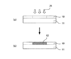
図2は、このような本実施態様の製造工程を説明するものである。ここで、10が有機半導体薄膜またはその前駆体薄膜、11が基板、12が特性改良した有機半導体膜または前駆体薄膜から変換された有機半導体膜、21が活性エネルギー線である。 FIG. 2 illustrates such a manufacturing process of the present embodiment. Here, 10 is an organic semiconductor thin film or a precursor thin film thereof, 11 is a substrate, 12 is an organic semiconductor film converted from an organic semiconductor film or a precursor thin film having improved characteristics, and 21 is an active energy ray.
図2に示すように、本実施態様においては、基板11上に形成された有機半導体薄膜またはその前駆体薄膜10に活性エネルギー線21を照射し(図2(a))、この基板11上で、これら薄膜を特性改良、または有機半導体膜に変換するようにしている(図2(b))。
As shown in FIG. 2, in this embodiment, the organic semiconductor thin film or the precursor
本実施態様は、このように有機半導体薄膜またはその前駆体薄膜が成膜された基板上でこれら薄膜の特性向上または変換を行うものであるので、有機半導体膜を形成するために他の部材を必要とせず、製造コストが安価であるという利点を有するものである。 Since the present embodiment is to improve or convert the characteristics of these thin films on the substrate on which the organic semiconductor thin film or the precursor thin film is formed, other members are required to form the organic semiconductor film. This has the advantage that it is not required and the manufacturing cost is low.
(第2実施態様)
一方、第2実施態様は、基板上に有機半導体薄膜またはその前駆体薄膜を成膜した後、活性エネルギー線を照射することにより、有機半導体薄膜の特性改良または前駆体薄膜を有機半導体膜に変換すると同時に、得られた有機半導体膜を他の基板上に昇華させ、上記薄膜が成膜された基板とは別の基板上に有機半導体膜を形成するものである。このように、本実施態様においては、上記薄膜が形成される基板と有機半導体膜が形成される基板とは異なるものである。
(Second embodiment)
On the other hand, in the second embodiment, after forming an organic semiconductor thin film or its precursor thin film on a substrate, irradiation with active energy rays improves the characteristics of the organic semiconductor thin film or converts the precursor thin film into an organic semiconductor film. Simultaneously, the obtained organic semiconductor film is sublimated on another substrate, and the organic semiconductor film is formed on a substrate different from the substrate on which the thin film is formed. Thus, in this embodiment, the substrate on which the thin film is formed and the substrate on which the organic semiconductor film is formed are different.
図3は、本実施態様の製造工程を説明するものであり、13が基板であり、10、11、12および21については、図2で示したものと同じである。
FIG. 3 illustrates a manufacturing process of the present embodiment.
図3に示すように、本実施態様においては、有機半導体薄膜またはその前駆体薄膜10とは反対側の基板11から活性エネルギー線21を照射し(図3(a))、有機半導体膜12を形成するとともに、得られた有機半導体膜12を基板13上に昇華させるようにしている。
As shown in FIG. 3, in the present embodiment, an
本実施態様は、このようにして有機半導体膜を、有機半導体薄膜またはその前駆体薄膜を成膜した基板とは異なる基板上に形成するものであるので、上述した第1実施態様に比べると製造コストがかかるものではある。しかしながら、有機半導体膜が形成される基板上には活性エネルギー線が照射されないため、有機半導体膜を形成する基板には熱伝導率や耐熱性等の制約が全くなく、基板材料の選択の幅が広がるという利点を有する。 In this embodiment, since the organic semiconductor film is formed on a substrate different from the substrate on which the organic semiconductor thin film or the precursor thin film is formed in this manner, the organic semiconductor film is manufactured in comparison with the first embodiment described above. It is costly. However, since active energy rays are not irradiated on the substrate on which the organic semiconductor film is formed, the substrate on which the organic semiconductor film is formed has no restrictions such as thermal conductivity and heat resistance, and the range of selection of the substrate material is limited. It has the advantage of spreading.
このように本発明の積層体の製造方法は2種類の実施態様を有するものである。 As described above, the method for producing a laminate of the present invention has two types of embodiments.
以下、このような本発明の積層体の製造方法について、まず有機半導体薄膜もしくは前駆体薄膜を形成する工程(以下、薄膜形成工程と称する場合がある。)と、活性エネルギー線を照射する工程(以下、照射工程と称する場合がある。)とに分けて説明する。 Hereinafter, in the method for manufacturing a laminate of the present invention, first, a step of forming an organic semiconductor thin film or a precursor thin film (hereinafter, may be referred to as a thin film forming step) and a step of irradiating active energy rays ( Hereinafter, it may be referred to as an irradiation step.).
1.薄膜形成工程
本発明においては、まず基板上に有機半導体薄膜もしくは前駆体薄膜を形成する薄膜形成工程が行われる。
1. Thin Film Formation Step In the present invention, first, a thin film formation step of forming an organic semiconductor thin film or a precursor thin film on a substrate is performed.
本発明における薄膜形成工程において用いられる薄膜形成方法は、上述した薄膜を容易に剥離することなく基板上に形成することができる方法であれば特に限定されるものではない。 The thin film forming method used in the thin film forming step in the present invention is not particularly limited as long as the thin film described above can be formed on a substrate without easily peeling.
したがって、有機半導体薄膜またはその前駆体薄膜が真空プロセスで形成できる場合には、真空プロセスを利用することもできる。このような真空プロセスの場合には、有機半導体またはその前駆体をルツボや金属のボートに入れて真空中で加熱し、基板に付着させる真空蒸着法を用いることができる。この際、真空度としては、1.3×10⁻¹Pa以下、好ましくは1.3×10⁻³Pa以下が望ましい。蒸着速度は通常0.001nm/秒以上、好ましくは、0.01nm/秒以上、ただし通常、10nm/秒以下、好ましくは、1nm/秒以下が用いられる。材料を蒸発させる方法としては、加熱の他、加速したアルゴン等のイオンを衝突させるスパッタ法も用いることができる。 Therefore, when the organic semiconductor thin film or its precursor thin film can be formed by a vacuum process, a vacuum process can also be used. In the case of such a vacuum process, a vacuum evaporation method in which an organic semiconductor or a precursor thereof is placed in a crucible or a metal boat, heated in a vacuum, and attached to a substrate can be used. At this time, the degree of vacuum is 1.3 × 10 −1 Pa or less, preferably 1.3 × 10 −3 Pa or less. The deposition rate is usually 0.001 nm / sec or more, preferably 0.01 nm / sec or more, but usually 10 nm / sec or less, preferably 1 nm / sec or less. As a method for evaporating the material, in addition to heating, a sputtering method in which accelerated ions such as argon are bombarded can also be used.
しかしながら、本発明においては、基材に熱を加えずに薄膜形成を行うことができ、かつ有機物のメリットを利用し、大容量の積層体を製造する場合にも低コストかつ簡便な方法で薄膜を形成できることから、有機半導体あるいはその前駆体を溶媒に溶解する等して液状とし、これを塗布して固化させる塗布プロセスを用いることが好ましい。 However, in the present invention, a thin film can be formed without applying heat to a substrate, and the thin film can be formed by a low-cost and simple method even when a large-capacity laminate is manufactured by utilizing the advantages of organic substances. It is preferable to use a coating process of dissolving the organic semiconductor or its precursor in a solvent or the like to form a liquid, and applying and solidifying the liquid.
特に、本発明においては、後述する照射工程において、光等の活性エネルギー線を照射することにより、基板に対して過剰な熱を加えることなく、前駆体薄膜を有機半導体膜としたり、有機半導体薄膜の特性を向上させたりするものであることから、薄膜形成工程においても基板に過剰な熱を加えることなく成膜できる成膜方法を用いることにより、耐熱性の比較的低い基板であっても各種電子デバイスの基板として用いることが可能となる点で好ましいといえる。 In particular, in the present invention, in the irradiation step described below, by irradiating active energy rays such as light without applying excessive heat to the substrate, the precursor thin film can be used as an organic semiconductor thin film or an organic semiconductor thin film. Even in the case of a substrate having a relatively low heat resistance, a film forming method capable of forming a film without applying excessive heat to the substrate in the thin film forming process is used. This can be said to be preferable in that it can be used as a substrate of an electronic device.
このような塗布プロセスにおいて用いられる塗工液としては、特に限定されるものではないが、通常は有機半導体あるいはその前駆体を溶媒に溶解した溶液を用いる。また、塗布方法としては、キャスティング、スピンコーティング、ディップコーティング、ブレードコーティング、ワイヤバーコーティング、スプレーコーティング等のコーティング法や、インクジェット印刷、スクリーン印刷、オフセット印刷、凸版印刷、フレキソ印刷等の印刷法、マイクロコンタクトプリンティング法等のソフトリソグラフィーの手法等、さらにはこれらの手法を複数組み合わせた方法を用いることができる。 The coating liquid used in such a coating process is not particularly limited, but usually a solution in which an organic semiconductor or a precursor thereof is dissolved in a solvent is used. The coating method includes coating methods such as casting, spin coating, dip coating, blade coating, wire bar coating, and spray coating, and printing methods such as inkjet printing, screen printing, offset printing, letterpress printing, flexographic printing, and the like. A method of soft lithography such as a contact printing method, or a method combining a plurality of these methods can be used.
また、塗布プロセスに類似の方法として、水面上に形成した単分子膜を基板に移し積層するラングミュアブロジェット法、液晶や融液状態の有機半導体もしくはその前駆体を、2枚の基板で挟んだ狭い間隙に毛管現象で導入する方法等も挙げることができる。 In addition, as a method similar to the coating process, a Langmuir-Blodgett method in which a monomolecular film formed on the water surface is transferred to a substrate and laminated, a liquid crystal or an organic semiconductor in a molten state or a precursor thereof is sandwiched between two substrates. A method of introducing into a narrow gap by capillary action can also be mentioned.
以下、本工程に用いる有機半導体、前駆体、および基板について説明する。 Hereinafter, the organic semiconductor, the precursor, and the substrate used in this step will be described.
(1)有機半導体
本発明において、このような薄膜形成工程において形成される有機半導体薄膜の材料として用いられる有機半導体は、後述する照射工程において活性エネルギー線を照射されて特性が改良されるものであれば特に限定されるものではないが、特に光を照射されて発生する熱により特性が改良される有機半導体が好ましいものであるといえる。
(1) Organic Semiconductor In the present invention, an organic semiconductor used as a material of an organic semiconductor thin film formed in such a thin film forming step is one whose properties are improved by being irradiated with active energy rays in an irradiation step described later. There is no particular limitation as long as it is present, but it can be said that an organic semiconductor whose characteristics are particularly improved by heat generated by irradiation with light is preferable.
このような有機半導体としては、例えば、α−セキシチオフェン、ジアルキルセキシチオフェンに代表される、チオフェン環を4個以上含むオリゴチオフェン類、あるいは、チオフェン環、ベンゼン環、フルオレン環、ナフタレン環、アントラセン環、チアゾール環、チアジアゾール環、ベンゾチアゾール環を合計4個以上連結したもの、ナフタレン、ペンタセン、ピレン、ペリレン、フラーレン等の縮合芳香族炭化水素、アントラジチオフェン、ジベンゾチエノビスチオフェン、α,α´−ビス(ジチエノ[3,2-b´:2´,3´-d]チオフェン)等の縮合チオフェンおよびその誘導体、ナフタレンテトラカルボン酸無水物、ナフタレンテトラカルボン酸ジイミド、ペリレンテトラカルボン酸無水物、ペリレンテトラカルボン酸ジイミド等の、芳香族カルボン酸無水物やそのイミド化物、銅フタロシアニン、パーフルオロ銅フタロシアニン、テトラベンゾポルフィリン及びその金属塩等の大環状化合物、ポリチオフェン、ポリフルオレン、ポリチエニレンビニレン、ポリフェニレンビニレン、ポリフェニレン、ポリアセチレン、ポリピロール、ポリアニリン等の共役高分子およびそれらの共重合体等が挙げられ、その中でも特に、レジオレギュラーポリチオフェンのような自己組織化を示すものや、ポリフルオレンやその共重合体に代表される液晶性を示す共役高分子等が好ましく挙げられる。 Examples of such an organic semiconductor include oligothiophenes having four or more thiophene rings, such as α-sexithiophene and dialkylsexithiophene, or thiophene rings, benzene rings, fluorene rings, naphthalene rings, Those in which a total of four or more anthracene rings, thiazole rings, thiadiazole rings, and benzothiazole rings are linked, condensed aromatic hydrocarbons such as naphthalene, pentacene, pyrene, perylene, fullerene, anthradithiophene, dibenzothienobisthiophene, α, α Condensed thiophenes such as' -bis (dithieno [3,2-b ': 2', 3'-d] thiophene) and derivatives thereof, naphthalenetetracarboxylic anhydride, naphthalenetetracarboxylic diimide, perylenetetracarboxylic anhydride And aromatic carmines such as perylenetetracarboxylic diimide Macrocyclic compounds such as acid anhydrides and imidates thereof, copper phthalocyanine, perfluorocopper phthalocyanine, tetrabenzoporphyrin and metal salts thereof, polythiophene, polyfluorene, polythienylenevinylene, polyphenylenevinylene, polyphenylene, polyacetylene, polypyrrole, polyaniline Conjugated polymers such as conjugated polymers and their copolymers, among which, among others, those exhibiting self-organization such as regioregular polythiophene, and conjugates exhibiting liquid crystallinity represented by polyfluorene and its copolymers Preferred are polymers and the like.
本工程においては、このような有機半導体を溶媒に溶解し、塗布し固化することにより有機半導体薄膜を形成する塗布プロセスによる方法が好ましいのであるが、この際用いられる溶媒としては、上述した有機半導体を溶解もしくは分散し得るものであれば特に限定されるものではない。具体的には、ヘキサン、ヘプタン、オクタン等の脂肪族炭化水素、トルエン、ベンゼン、キシレン、クロロベンゼン等の芳香族炭化水素、メタノール、エタノール、プロパノール、ブタノール等のアルコール類、アセトン、メチルエチルケトン、シクロペンタノン、シクロヘキサノン等のケトン類、低級エーテル類、酢酸エチル、酢酸ブチル等のエステル類、ピリジン、キノリン等の含窒素芳香族、クロロホルム、塩化メチレン、ジクロロエタン、トリクロロエタン、トリクロロエチレン等のハロゲン化炭化水素、ジエチルエーテル、テトラヒドロフラン、ジオキサン等のエーテル類、ジメチルホルムアミド、ジメチルアセトアミド等のアミド類等を用いることができる。 In this step, a method by a coating process of dissolving such an organic semiconductor in a solvent, and coating and solidifying to form an organic semiconductor thin film is preferable. Is not particularly limited as long as it can dissolve or disperse. Specifically, aliphatic hydrocarbons such as hexane, heptane and octane, aromatic hydrocarbons such as toluene, benzene, xylene and chlorobenzene, alcohols such as methanol, ethanol, propanol and butanol, acetone, methyl ethyl ketone and cyclopentanone , Ketones such as cyclohexanone, lower ethers, esters such as ethyl acetate and butyl acetate, nitrogen-containing aromatics such as pyridine and quinoline, halogenated hydrocarbons such as chloroform, methylene chloride, dichloroethane, trichloroethane and trichloroethylene, and diethyl ether And ethers such as tetrahydrofuran and dioxane, and amides such as dimethylformamide and dimethylacetamide.
(2)前駆体
また、このような薄膜形成工程において形成される前駆体薄膜の材料として用いられる前駆体としては、後述する照射工程において活性エネルギー線を照射されて有機半導体となるものであれば特に限定されるものではないが、特に光を照射されて発生する熱により一部または全部が完全に有機半導体に変換される前駆体が好ましいものであり、中でも塗布による薄膜形成を可能とし、低コストかつ簡便な方法で有機半導体膜を形成できることから、前駆体としては、有機溶媒に対する溶解性の高いものが好ましい。
(2) Precursor As a precursor used as a material of a precursor thin film formed in such a thin film forming step, a precursor which is irradiated with active energy rays in an irradiation step described later to become an organic semiconductor is used. Although it is not particularly limited, a precursor that is partially or wholly completely converted into an organic semiconductor by heat generated by irradiation with light is particularly preferable. As the organic semiconductor film can be formed by a cost and simple method, a precursor having high solubility in an organic solvent is preferable as the precursor.
このような前駆体としては、下記の構造式で示した化合物等を好ましく挙げることができる。これらの前駆体は後述する照射工程において照射される光により発生する熱により有機半導体へ変換される化合物の一例である。 Preferred examples of such a precursor include compounds represented by the following structural formulas. These precursors are an example of a compound that is converted into an organic semiconductor by heat generated by light irradiated in an irradiation step described below.

これらの前駆体を溶解する溶媒としては、特に限定されるものではないが、上述した有機半導体の欄で説明した溶媒を用いることができる。 Although the solvent for dissolving these precursors is not particularly limited, the solvents described in the section of the organic semiconductor described above can be used.
(3)基板
本工程において、上述した有機半導体や前駆体により有機半導体薄膜もしくは前駆体薄膜が形成される基板の材料は特に限定されるものではなく、積層体を製造する実施態様により適宜決定すればよい。
(3) Substrate In this step, the material of the substrate on which the organic semiconductor thin film or the precursor thin film is formed by the above-described organic semiconductor or precursor is not particularly limited, and may be appropriately determined depending on the embodiment for manufacturing the laminate. Just fine.
このような材料としては、例えば、樹脂からなる板やフィルム、紙、合成紙、ガラス、セラミックなどの絶縁性材料、金属や合金などの導電性基板上にコーティング等により絶縁層を形成したもの、樹脂と無機材料など各種組合せからなる複合材等が挙げられる。これらの中でも、ガラス、セラミックなどの絶縁性材料、樹脂からなる板やフィルム、紙、合成紙が好ましい。これらの材料は熱伝導率が比較的低く、熱が拡散しにくいため、照射エネルギーを有効利用できるからである。また、樹脂材料や紙を用いると、素子に可撓性を持たせることができ、得られる積層体が軽量で柔軟なものとなることから特に好ましい材料であるといえる。このような基板に用いる樹脂材料として、好ましく挙げられるのは、ポリエチレンテレフタレート、ポリスルホン、ポリエーテルスルホン、ポリイミド、ナイロン、ポリスチレン、ポリカーボネート、ポリウレタン、ポリエチレンナフタレート、ポリ塩化ビニル、エポキシ樹脂、フェノール樹脂、ノボラック樹脂、アクリル樹脂、シロキサン樹脂等である。 As such a material, for example, a plate or film made of resin, paper, synthetic paper, glass, an insulating material such as ceramic, a material obtained by forming an insulating layer on a conductive substrate such as a metal or an alloy by coating or the like, A composite material composed of various combinations such as a resin and an inorganic material is exemplified. Among these, a plate or film made of an insulating material such as glass or ceramic, or a resin, paper, or synthetic paper is preferable. This is because these materials have a relatively low thermal conductivity and do not easily diffuse heat, so that irradiation energy can be effectively used. In addition, when a resin material or paper is used, the element can be made flexible, and the obtained laminate is light and flexible, which is a particularly preferable material. Preferred examples of the resin material used for such a substrate include polyethylene terephthalate, polysulfone, polyether sulfone, polyimide, nylon, polystyrene, polycarbonate, polyurethane, polyethylene naphthalate, polyvinyl chloride, epoxy resin, phenol resin, and novolak. Resin, acrylic resin, siloxane resin and the like.
本発明においては、中でも比較的耐熱性の低い材料で形成された基材を用いることが好ましい。本発明においては、後述する照射工程において活性エネルギー線を照射することにより、前駆体を有機半導体にしたり、有機半導体の特性を向上させたりするものであり、基板に対して過剰な加熱が加えられない点に利点を有するものである。したがって、このような利点を活かすことができ、かつ通常は安価な比較的耐熱性の低い材料で形成された基材とすることが好ましいのである。 In the present invention, it is particularly preferable to use a substrate formed of a material having relatively low heat resistance. In the present invention, by irradiating an active energy ray in an irradiation step described later, the precursor is made into an organic semiconductor, or the characteristics of the organic semiconductor are improved, and excessive heating is applied to the substrate. There is an advantage in that there is no. Therefore, it is preferable to use a base material made of an inexpensive and relatively low heat-resistant material that can take advantage of such advantages.
具体的には、Tgが200℃以下、特に150℃以下の樹脂で形成された基材が好適に用いられる。このような耐熱性の比較的低い樹脂性の材料としては、ポリエチレンテレフタレート、ポリカーボネート、ポリスチレン、ポリエーテルスルホン、ポリウレタン、ポリエチレンナフタレート、ポリ塩化ビニル等を挙げることができる。 Specifically, a substrate formed of a resin having a Tg of 200 ° C. or lower, particularly 150 ° C. or lower is suitably used. Examples of such a resin material having relatively low heat resistance include polyethylene terephthalate, polycarbonate, polystyrene, polyether sulfone, polyurethane, polyethylene naphthalate, and polyvinyl chloride.
2.照射工程
次に、本発明においては、上記薄膜形成工程において形成された有機半導体薄膜もしくは前駆体薄膜に対して活性エネルギー線を照射する照射工程が行われる。この照射工程により、上述の薄膜形成工程において形成された有機半導体薄膜または前駆体薄膜は、活性エネルギー線を照射されることにより、有機半導体薄膜であればその特性を改良することができ、前駆体薄膜であれば有機半導体膜への変換を行うことができる。
2. Irradiation Step Next, in the present invention, an irradiation step of irradiating the organic semiconductor thin film or the precursor thin film formed in the thin film forming step with active energy rays is performed. By the irradiation step, the organic semiconductor thin film or the precursor thin film formed in the above-described thin film forming step can be irradiated with an active energy ray to improve the characteristics of the organic semiconductor thin film if it is an organic semiconductor thin film. If it is a thin film, conversion to an organic semiconductor film can be performed.
また、上述した第2実施態様により有機半導体膜を含む積層体を製造する場合には、この照射工程において、有機半導体薄膜の特性改良や、前駆体薄膜の有機半導体膜への変換を行うとともに、得られた有機半導体膜を他の基板上に昇華させることができる。 In the case of manufacturing a laminate including an organic semiconductor film according to the second embodiment described above, in this irradiation step, while improving the characteristics of the organic semiconductor thin film and converting the precursor thin film into an organic semiconductor film, The obtained organic semiconductor film can be sublimated on another substrate.
活性エネルギー線の照射は、有機半導体薄膜または前駆体薄膜に直接的または間接的に作用するものであればよい。「間接的に」とは、例えば、後で詳述する光吸収層が形成され、活性エネルギー線として光を照射したような場合に、照射された光エネルギーを、まず光吸収層が吸収し、それを熱エネルギーに変換した後、薄膜に作用するような場合をいう。 Irradiation with an active energy ray may be any as long as it directly or indirectly acts on the organic semiconductor thin film or the precursor thin film. `` Indirectly '' means, for example, when a light absorbing layer described in detail below is formed and light is irradiated as an active energy ray, the irradiated light energy is first absorbed by the light absorbing layer, After converting it into heat energy, it acts on the thin film.
ここで、「活性エネルギー線」とは、上記有機半導体薄膜の特性改良または前駆体薄膜の有機半導体への変換を瞬時に行えるものであれば特に限定されず、遠紫外線、紫外線、近紫外線、赤外線等の光、X線、γ線、マイクロ波等の光以外の電磁波の他、電子線、プロトン線、中性子線等を含む広い概念である。 Here, the “active energy ray” is not particularly limited as long as the property improvement of the organic semiconductor thin film or the conversion of the precursor thin film to the organic semiconductor can be performed instantaneously. This is a broad concept including electromagnetic waves other than light such as X-rays, γ-rays, and microwaves, as well as electron beams, proton beams, and neutron beams.
本発明においては、取扱いの容易性等の観点から活性エネルギー線が光であることが好ましく、中でも後述する各種パラメータ、すなわち光の照射条件の制御が容易である点から、レーザ光を用いることが特に好ましい。 In the present invention, it is preferable that the active energy ray is light from the viewpoint of ease of handling and the like, and among them, various parameters described later, that is, laser light is preferably used because it is easy to control the light irradiation conditions. Particularly preferred.
また、本発明においては、上述した活性エネルギー線を有機半導体薄膜もしくは前駆体薄膜に照射し、これが熱に変換されて上記有機半導体薄膜もしくは前駆体薄膜に作用し、上述したような有機半導体薄膜の特性の向上や前駆体薄膜の有機半導体膜への変換が行われるものであることが好ましい。活性エネルギー線が薄膜側から照射される場合には、照射された領域において熱に変換され、これにより有機半導体薄膜の特性の向上や前駆体薄膜の有機半導体膜への変換を行うことができ、基板に対して過剰な加熱を行うことなく上記反応を行うことが可能となる。したがって、基板が比較的耐熱性の低い樹脂製であっても用いることができる。 Further, in the present invention, the organic semiconductor thin film or the precursor thin film is irradiated with the above-mentioned active energy ray, which is converted into heat and acts on the organic semiconductor thin film or the precursor thin film. It is preferable that the properties be improved and the precursor thin film be converted to an organic semiconductor film. When the active energy ray is irradiated from the thin film side, it is converted into heat in the irradiated region, thereby improving the characteristics of the organic semiconductor thin film and converting the precursor thin film to the organic semiconductor film, The above reaction can be performed without excessive heating of the substrate. Therefore, even if the substrate is made of a resin having relatively low heat resistance, it can be used.
また、上記第2実施態様の場合のように、活性エネルギー線が基板側から照射される場合には、照射された領域において熱に変換され、基板の熱伝導により、有機半導体薄膜の特性の向上や前駆体薄膜の有機半導体膜への変換を行うとともに、他の基板上に得られた有機半導体膜を昇華させることができるので、この有機半導体膜を形成する基板には活性エネルギー線が照射されないため、さらに耐熱性の低い基板材料を用いることも可能である。 When the active energy ray is irradiated from the substrate side as in the case of the second embodiment, the active energy ray is converted into heat in the irradiated area, and the heat conduction of the substrate improves the characteristics of the organic semiconductor thin film. And a precursor thin film can be converted to an organic semiconductor film, and the organic semiconductor film obtained on another substrate can be sublimated, so that the substrate on which this organic semiconductor film is formed is not irradiated with active energy rays. Therefore, a substrate material having even lower heat resistance can be used.
本発明においては、中でも活性エネルギー線として光を用い、照射工程において照射された光が熱に変換されるように用いられる方法が特に好ましい方法であるといえる。 In the present invention, a method in which light is used as an active energy ray and the light irradiated in the irradiation step is converted into heat is a particularly preferable method.
なお、本発明において、活性エネルギー線は上述した薄膜形成工程において形成された薄膜の全面にわたって照射しても、その一部にパターン状に照射してもよい。パターン状に照射することにより、例えば薄膜が前駆体薄膜の場合はパターン状に有機半導体とした積層体を得ることが可能となり、また薄膜が有機半導体薄膜である場合は、パターン状に特性の変化した有機半導体膜を有する積層体を得ることができる。 In the present invention, the active energy ray may be irradiated on the entire surface of the thin film formed in the above-described thin film forming step or may be partially irradiated on the thin film. By irradiating in a pattern, for example, when the thin film is a precursor thin film, it is possible to obtain a laminate in which an organic semiconductor is formed in a pattern, and when the thin film is an organic semiconductor thin film, a characteristic change occurs in a pattern. Thus, a laminate having the organic semiconductor film can be obtained.
以下、このような活性エネルギー線として光を用いた場合の、各種照射条件について説明する。 Hereinafter, various irradiation conditions when light is used as such an active energy ray will be described.
(1)光の波長
本発明に用いる光の波長は、一般的に光と称される波長の範囲内であれば特に限定されるものではなく、具体的には100nm以上、100μm以下程度のものが用いられる。
(1) Wavelength of Light The wavelength of light used in the present invention is not particularly limited as long as it is within a wavelength range generally called light, and specifically, about 100 nm or more and 100 μm or less. Is used.
光照射は、上述したように薄膜に直接的または間接的に作用しうるものであれば特に限定されないが、有機半導体薄膜の特性改良または前駆体薄膜の有機半導体膜への変換をより効果的に行うことができることから、薄膜に直接作用しうる方法、具体的には有機半導体薄膜もしくは前駆体薄膜に直接照射する方法が好ましい。この場合の光の波長としては、有機半導体薄膜もしくは前駆体薄膜が吸収する波長、特に薄膜の吸収が大きい波長が好ましく、積層体の他の構成材料による吸収が小さい波長であることが好ましい。他の材料、特に基板へのダメージを防止することができるからである。 Light irradiation is not particularly limited as long as it can directly or indirectly act on the thin film as described above, but more effectively improves the characteristics of the organic semiconductor thin film or converts the precursor thin film into the organic semiconductor film. Since it can be performed, a method capable of directly acting on a thin film, specifically, a method of directly irradiating an organic semiconductor thin film or a precursor thin film is preferable. In this case, the wavelength of the light is preferably a wavelength absorbed by the organic semiconductor thin film or the precursor thin film, particularly a wavelength at which the absorption of the thin film is large, and a wavelength at which absorption by other constituent materials of the laminate is small. This is because damage to other materials, particularly to the substrate, can be prevented.
なお、上述した第2実施態様を用いる場合には、このように積層体の他の構成材料へのダメージを考慮する必要はない。 When the second embodiment described above is used, it is not necessary to consider the damage to other constituent materials of the laminate in this way.
具体的には、有機半導体薄膜または前駆体薄膜の吸収係数(α)が1×10⁴(m−1)以上のものが通常用いられ、好ましくは1×10⁵(m−1)以上、さらに好ましくは1×10⁶(m−1)以上の波長の光が用いられる。なお、このαは、膜の透過率をT(%)、膜厚をd(m)とするとα=(1/d)ln(100/T)で与えられる値である。 Specifically, an organic semiconductor thin film or a precursor thin film having an absorption coefficient (α) of 1 × 10 4 (m −1 ) or more is generally used, preferably 1 × 10 5 (m −1 ) or more, Preferably, light having a wavelength of 1 × 10 6 (m −1 ) or more is used. Here, α is a value given by α = (1 / d) ln (100 / T) where T (%) is the transmittance of the film and d (m) is the film thickness.
本発明においては、上述したように光を照射することにより、有機半導体薄膜または前駆体薄膜が加熱されることが好ましく、特に、これら薄膜の表面を瞬時に加熱できるものであることが好ましい。有機半導体の特性改良または前駆体から有機半導体への変換をより効果的に行えるためである。 In the present invention, it is preferable that the organic semiconductor thin film or the precursor thin film is heated by irradiating light as described above, and it is particularly preferable that the surface of these thin films can be heated instantaneously. This is because the characteristics of the organic semiconductor can be improved or the conversion from the precursor to the organic semiconductor can be more effectively performed.
ここで、「加熱」とは、室温(25℃)より温度を10℃以上高くすることをいい、加熱温度は、好ましくは80℃以上、より好ましくは100℃以上とする。ただし、あまり高温にすると薄膜自体がダメージを受ける場合があるので、通常、500℃以下、好ましくは400℃以下、より好ましくは300℃以下にする。 Here, “heating” refers to raising the temperature by at least 10 ° C. from room temperature (25 ° C.), and the heating temperature is preferably at least 80 ° C., more preferably at least 100 ° C. However, if the temperature is too high, the thin film itself may be damaged. Therefore, the temperature is usually set to 500 ° C. or lower, preferably 400 ° C. or lower, more preferably 300 ° C. or lower.
(2)光照射時間
本発明における光の照射時間は、有機半導体の種類により任意に選択でき、有機半導体の特性改良または前駆体から有機半導体への変換を十分に行うことができ、また、上述した第2実施態様により上記積層体を製造する場合には、得られた有機半導体膜を他の基板上に昇華させることができる時間であればよいが、薄膜やその周辺部へのダメージを抑制するためにはできるだけ短時間で行うことが好ましく、薄膜の一領域に連続して光を照射する時間は、通常100ms以下であることが好ましく、より好ましくは10ms以下、さらに好ましくは1ms以下、特に100μs以下、中でも10μs以下、とりわけ5μs以下であることが好ましく、最も好ましくは1μs以下である。ただし、照射時間は、通常10fs以上、好ましくは100fs以上、さらに好ましくは1ns以上とする。これは、吸収によって生じる励起状態の寿命より短い時間では吸収のブリーチングが起こり、有効に吸収ができなくなってしまうことや、ピーク強度の強いレーザーでは、各種の非線形光学効果が起こり、所望の光照射の効果が有効に利用できなくなるためである。
(2) Light Irradiation Time The light irradiation time in the present invention can be arbitrarily selected depending on the type of the organic semiconductor, and can improve the characteristics of the organic semiconductor or sufficiently convert the precursor to the organic semiconductor. In the case of manufacturing the above-mentioned laminate according to the second embodiment described above, any time may be used as long as the obtained organic semiconductor film can be sublimated on another substrate, but the damage to the thin film and its peripheral portion is suppressed. In order to perform the irradiation, it is preferable to perform the irradiation in as short a time as possible, and the time for continuously irradiating one region of the thin film is usually preferably 100 ms or less, more preferably 10 ms or less, further more preferably 1 ms or less, particularly preferably 1 ms or less. It is preferably 100 μs or less, more preferably 10 μs or less, especially 5 μs or less, and most preferably 1 μs or less. However, the irradiation time is usually at least 10 fs, preferably at least 100 fs, more preferably at least 1 ns. This is because the bleaching of the absorption occurs in a time shorter than the lifetime of the excited state caused by the absorption, which makes it impossible to absorb the light effectively. This is because the effect of irradiation cannot be used effectively.
なお、光照射の回数は、1回に限定されるものではなく、必要に応じて複数回照射してもよい。 Note that the number of light irradiations is not limited to one, and irradiation may be performed a plurality of times as necessary.
光照射時間は、薄膜の厚さ、熱拡散係数、材料等により大きく異なるものであり、一概に決めることはできないが、目安として、下記の関係式を用いることができる。 The light irradiation time varies greatly depending on the thickness of the thin film, the thermal diffusion coefficient, the material, and the like, and cannot be unconditionally determined. However, the following relational expression can be used as a guide.
すなわち、有機半導体薄膜または前駆体薄膜の厚さをa(m)、熱拡散係数をκ(m2/s)とおく。このaとκで決まる時間t0=a2/κ(s)を定義する。薄膜が一定速度で加熱された場合、時間が加熱開始からt0までの時間では熱は膜外にはほとんど拡散せずに膜内に蓄積するため、加熱時間に比例して膜の温度が上昇する。この時間を過ぎると熱が層外に伝わることになり、膜の温度は時間の平方根に比例して上昇するようになり、膜周辺の温度も上昇するようになる。電子デバイスの半導体層として用いられる有機半導体膜は通常1μmより薄く、基板は100μm程度あることが多いので、この周辺への影響はt0の100倍程度の時間までは大きくないことが期待される。もちろん短ければ短いほど好ましく、より好ましくは10倍以内である。一方、有機物の熱拡散係数は、約1×10−7(m2/s)程度の値であるので、t0はa2×107程度になり、その100倍の時間はa2×109秒になる。 That is, the thickness of the organic semiconductor thin film or the precursor thin film is set to a (m), and the thermal diffusion coefficient is set to κ (m 2 / s). A time t 0 = a 2 / κ (s) determined by a and κ is defined. If the thin film is heated at a constant rate, because time to accumulate in the membrane with little diffuse the heat extramembrane in the time from the start of heating to t 0, the temperature of the film in proportion to the heating time is increased I do. After this time, heat is transferred out of the layer, the temperature of the film increases in proportion to the square root of time, and the temperature around the film also increases. The organic semiconductor film used as semiconductor layers of electronic devices thinner than normal 1 [mu] m, since the substrate is often about 100 [mu] m, it is expected that impact on the surrounding is not large up to 100 times the time t 0 . Of course, the shorter the better, the better, more preferably within 10 times. On the other hand, since the thermal diffusion coefficient of the organic substance is about 1 × 10 −7 (m 2 / s), t 0 is about a 2 × 10 7 , and 100 times as long as a 2 × 10 7 9 seconds.
このような観点から、本発明における光の照射時間を規定すると、好ましくは、a2×109秒以下であり、特に10μs以下、中でも1μs以下とすることが好ましい。なお、この場合の下限は、上述したものと同様である。 From this point of view, when defining the light irradiation time in the present invention, preferably, not more than a 2 × 10 9 seconds, especially 10μs or less, it is preferable to inter alia 1μs or less. Note that the lower limit in this case is the same as that described above.
なお、薄膜の膜厚を0.1μmとすると、a2×109は10μsとなり、10μs以内で光照射すれば有機半導体またはその前駆体の近傍のみ加熱することができる。これは、パルスレーザーを用いれば十分可能な時間であり、連続光でも強く絞って走査することによりこのような光照射時間を達成することが可能である。 If the thickness of the thin film is 0.1 μm, a 2 × 10 9 becomes 10 μs, and if light irradiation is performed within 10 μs, only the vicinity of the organic semiconductor or its precursor can be heated. This is a sufficiently long time if a pulsed laser is used, and it is possible to achieve such a light irradiation time by performing scanning with a strong stop even with continuous light.
また、薄膜に電極が接していることがあるが、この部分も光照射により加熱することが可能である。そのような場合には光照射条件をそれに適したものに調整することが好ましい。電極に用いられている金属の熱拡散係数は大きいので、金属内の熱伝導は有機物に比較して非常に大きくなる。よって、光照射スポットが小さい場合には横方向の熱拡散が大きくなり、温度が上がりにくくなる。しかしながら、光照射部分が横方向の熱拡散長に対して十分に大きく、その伝熱の効果が大きくなく、かつ金属電極が有機半導体と同じ程度の膜厚であれば、金属の体積熱容量は有機物とあまり変わらないため、必要とされる光エネルギーは有機半導体の膜厚が増加したと考えた照射量と同程度と見積もることができる。したがって、薄膜に接している電極は、薄膜と同等あるいはそれよりも薄くし、光照射するスポットを横方向の拡散よりも十分に大きくするために、1μm以上、好ましくは10μm以上に大きくするか、十分に短い照射時間、例えば1μs以下、好ましくは100ns以下の短い照射時間で照射することが好ましい。 Further, the electrode may be in contact with the thin film, and this portion can be heated by light irradiation. In such a case, it is preferable to adjust the light irradiation conditions to those suitable for it. Since the metal used for the electrode has a large thermal diffusion coefficient, the heat conduction in the metal is much larger than that of an organic substance. Therefore, when the light irradiation spot is small, the thermal diffusion in the lateral direction increases, and the temperature does not easily rise. However, if the light-irradiated portion is sufficiently large with respect to the thermal diffusion length in the horizontal direction, the heat transfer effect is not large, and the metal electrode has a film thickness similar to that of the organic semiconductor, the volumetric heat capacity of the metal will not Therefore, the required light energy can be estimated to be about the same as the irradiation dose that is considered to increase the thickness of the organic semiconductor. Therefore, the electrode in contact with the thin film is made equal to or thinner than the thin film, and in order to make the spot irradiated with light sufficiently larger than the diffusion in the lateral direction, it is increased to 1 μm or more, preferably to 10 μm or more, Irradiation is preferably performed for a sufficiently short irradiation time, for example, 1 μs or less, preferably 100 ns or less.
(3)光の強度
照射する光の強度は、有機半導体が特性改良するか、その前駆体が有機半導体に変化する温度以上になるように調整する必要がある。また、上述した第2実施態様により上記積層体を製造する場合には、得られる有機半導体膜が他の基板上に昇華できる温度以上になるように調整する必要もある。光強度が弱すぎると目的の効果が得られず、強すぎると薄膜自体や基板等の周辺部へのダメージを引き起こすことがあるからである。
(3) Light Intensity The irradiation light intensity needs to be adjusted so that the characteristics of the organic semiconductor improve or the temperature at which the precursor changes to an organic semiconductor or higher. In the case where the above-described laminate is manufactured according to the above-described second embodiment, it is necessary to adjust the temperature so that the obtained organic semiconductor film can be sublimated above another substrate. If the light intensity is too low, the intended effect cannot be obtained, and if the light intensity is too high, damage to the thin film itself and peripheral parts such as the substrate may be caused.
照射する光の強度は、有機半導体の種類によって適宜選択でき、到達温度や熱拡散係数、吸収係数により大きく異なるが、照射光のパワー密度は100μJ/cm2以上が好ましく、さらに好ましくは1mJ/cm2以上である。また、100kJ/cm2以下が好ましく、さらに好ましくは100J/cm2以下である。特に吸収係数が1×107(m−1)以上の場合は1〜10J/cm2程度であることが好ましく、1×107〜1×105(m−1)の場合は100mJ/cm2〜100J/cm2程度であることが好ましく、1×105(m−1)以下の場合は10J/cm2〜100kJ/cm2程度であることが好ましい。
The intensity of the irradiation light can be appropriately selected depending on the type of the organic semiconductor, and greatly varies depending on the attained temperature, the thermal diffusion coefficient, and the absorption coefficient. The power density of the irradiation light is preferably 100 μJ / cm 2 or more, more preferably 1 mJ /
一度の照射で十分に変化しない場合には照射を繰り返すことができる。その際に照射の間隔は照射時間に対して100倍以上になるように十分長くとり、熱が蓄積しないようにする必要がある。 Irradiation can be repeated if a single irradiation does not change sufficiently. At that time, the irradiation interval needs to be sufficiently long so as to be 100 times or more the irradiation time, so that heat does not accumulate.
(4)光源
利用できる光源としては、上述したような波長の光を発することができる公知の光源の中から適宜選択することができる。中でも、光照射時間の制御が容易であることから、レーザ光の光源が好適に用いられる。
(4) Light Source The light source that can be used can be appropriately selected from known light sources that can emit light having the above-described wavelength. Above all, a light source of laser light is preferably used because the light irradiation time can be easily controlled.
レーザ光としては、Nd:YAGレーザおよびその第二あるいは第三高調波、アルゴンイオンレーザー、チタンサファイアレーザー、エキシマレーザー、半導体レーザ、色素レーザ、窒素レーザ、炭酸ガスレーザー、キセノンフラッシュランプ等を用いることができる。必要であればレンズで集光して光パワー密度を向上させることができる。 As a laser beam, use is made of a Nd: YAG laser and its second or third harmonic, an argon ion laser, a titanium sapphire laser, an excimer laser, a semiconductor laser, a dye laser, a nitrogen laser, a carbon dioxide laser, a xenon flash lamp, etc. Can be. If necessary, the light can be collected by a lens to improve the optical power density.
特に、高いパワーの光を短時間照射するには、パルスレーザーやフラッシュランプのような、パルス光を利用するのが好ましい。このような光源としては、パルスQスイッチNd:YAGレーザやチタンサファイアレーザー、エキシマレーザー等が挙げられる。 In particular, to irradiate high-power light for a short time, it is preferable to use pulsed light such as a pulsed laser or a flash lamp. Examples of such a light source include a pulse Q switch Nd: YAG laser, a titanium sapphire laser, an excimer laser, and the like.
また、連続光でもレンズで集光して光パワー密度を上げ、かつ照射スポットを高速で走査することにより、1点あたりの照射時間を十分に短くすることができる。例えば、連続発振している半導体レーザやアルゴンイオンレーザー、Nd:YAGレーザ、チタンサファイアレーザー等をレンズで10μm以下のスポットに絞り、レーザあるいは照射する膜を線速度10m毎秒で走査すれば、1点当たりの照射時間は1μsに調整できる。この走査には、膜を面内で高速回転させる方法や、ドラムに膜を巻きつけてドラムの軸の周りに回転させる方法、ポリゴンミラーでレーザ光の反射角を高速で変化させて走査する方法、音波による光の回折を利用して走査する方法等を用いることができる。 Further, even if continuous light is condensed by a lens to increase the light power density and scan the irradiation spot at high speed, the irradiation time per point can be sufficiently reduced. For example, a continuously oscillating semiconductor laser, argon ion laser, Nd: YAG laser, titanium sapphire laser, or the like is squeezed by a lens to a spot of 10 μm or less, and a laser or a film to be irradiated is scanned at a linear velocity of 10 m / sec. The irradiation time per hit can be adjusted to 1 μs. For this scanning, a method of rotating the film at high speed in the plane, a method of winding the film around the drum and rotating it around the axis of the drum, and a method of changing the reflection angle of the laser light with a polygon mirror at a high speed for scanning For example, a scanning method utilizing diffraction of light by a sound wave can be used.
(5)他の加熱源との組み合わせ
光照射と他の条件を組み合わせることも可能である。例えば、積層体全体が耐える温度で加熱しながら光照射を組み合わせることができる。また、2種類以上の波長の光を照射したり、照射する光の波長を変化させることや、加熱反応を促進するために、酸やアルカリ等の化学物質を気体あるいは液体、あるいは他の物質や溶媒との混合物(混合気体、溶液)と接触させる方法を組み合わせることができる。
(5) Combination with Other Heat Sources It is also possible to combine light irradiation with other conditions. For example, light irradiation can be combined while heating at a temperature at which the entire laminate can withstand. In addition, in order to irradiate light of two or more wavelengths, to change the wavelength of the irradiating light, and to promote a heating reaction, a chemical substance such as an acid or an alkali is converted into a gas or liquid, or another substance or the like. The method of contacting with a mixture (mixture gas, solution) with a solvent can be combined.
3.その他の工程
本発明の有機半導体膜を含む積層体の製造方法は、少なくとも上述した薄膜形成工程および照射工程を有するものであればよく、必要に応じて種々の他の工程が行われてもよい。
3. Other Steps The method for producing a laminate including the organic semiconductor film of the present invention may have at least the thin film forming step and the irradiation step described above, and various other steps may be performed as necessary. .
具体的には、上記薄膜形成工程の前に、基板上に種々の機能層が形成される機能層形成工程が行われていてもよい。具体的には、絶縁体層やゲート電極層、さらには、熱遮断層を形成する工程を有するものであってもよい。また、有機半導体膜に隣接するように光吸収層を形成する光吸収層形成工程を上記照射工程の前に行ってもよい。なお、光吸収層を形成する場合は、必要に応じて上記照射工程の後、その全部もしくは一部を除去する光吸収層除去工程を行ってもよい。 Specifically, before the thin film forming step, a functional layer forming step of forming various functional layers on the substrate may be performed. Specifically, the method may include a step of forming an insulator layer, a gate electrode layer, and a heat blocking layer. Further, a light absorbing layer forming step of forming a light absorbing layer so as to be adjacent to the organic semiconductor film may be performed before the irradiation step. When the light absorbing layer is formed, a light absorbing layer removing step of removing all or a part of the light absorbing layer may be performed after the irradiation step, if necessary.
上記熱遮断層や光吸収層等の材料や形成方法に関しては、次に説明する「B.積層体」の欄で詳述するものと同様であるので、ここでの説明は省略する。 The materials and forming methods of the heat-blocking layer and the light-absorbing layer are the same as those described in detail in the section of “B.
4.得られる有機半導体膜を含む積層体
このようにして得られる有機半導体膜を含む積層体は、少なくとも基板と有機半導体膜とを有しており、軽量で壊れにくく、低コストかつ簡便な方法で製造できることから、後述するように電子デバイスに好適に用いられ、特に電界効果トランジスタに用いられることが好ましい。
4. The laminate including the obtained organic semiconductor film The laminate including the organic semiconductor film thus obtained has at least a substrate and an organic semiconductor film, is lightweight, is not easily broken, and is manufactured by a low-cost and simple method. Because it can be used, it is preferably used for an electronic device as described later, and particularly preferably used for a field effect transistor.
本発明の電子デバイスは、上述した積層体の製造方法により得られる積層体を用いるものであるので、有機半導体膜の特性向上を充分に行うことができ、特にキャリア移動度が高い半導体膜を作成できる。したがって電子デバイスの中でも高キャリア移動度が求められる電界効果トランジスタに用いることにより、より高い効果を得ることができるからである。 Since the electronic device of the present invention uses the laminate obtained by the above-described method for producing a laminate, the characteristics of the organic semiconductor film can be sufficiently improved, and a semiconductor film having particularly high carrier mobility can be formed. it can. Therefore, a higher effect can be obtained by using a field-effect transistor requiring high carrier mobility among electronic devices.
有機半導体またはその前駆体からなる薄膜は、活性エネルギー線照射により、有機半導体へ変換させることができるだけでなく、所望のレベルにまで特性を改良することができるものであり、また、材料のバリエーションが豊富であることから、無機半導体では実現できない様々な機能を組み合わせた高性能の電子デバイスを製造することができる。 A thin film composed of an organic semiconductor or a precursor thereof can be converted into an organic semiconductor by irradiation with active energy rays, and can also be improved in properties to a desired level. Because of the abundance, a high-performance electronic device combining various functions that cannot be realized with an inorganic semiconductor can be manufactured.
B.積層体
本発明の有機半導体膜を有する積層体は、基板と、上記基板上に形成された断熱性および耐熱性を有する熱遮断層と、上記熱遮断層上に形成された有機半導体膜とを有することを特徴とするものである。
B. The laminate having the organic semiconductor film of the present invention includes a substrate, a heat insulation layer having heat insulation and heat resistance formed on the substrate, and an organic semiconductor film formed on the heat insulation layer. It is characterized by having.
このように、本発明の積層体は基板と有機半導体膜との間に熱遮断層を有するものであるので、例えば有機半導体膜を製造する際に、予め溶媒に可溶な前駆体が溶解した前駆体形成用塗工液を塗布し固化させて前駆体薄膜を形成し、前駆体薄膜側から光を照射し、これにより加熱して前駆体を有機半導体とするような製法を用いた場合でも、前駆体が加熱される際に熱遮断層により熱が基板側に伝達されにくい。したがって、比較的耐熱性の低い、安価な汎用樹脂製の基板を用いた場合でも問題無く製造することができるといった利点を有する。 As described above, since the laminate of the present invention has a thermal barrier layer between the substrate and the organic semiconductor film, for example, when manufacturing an organic semiconductor film, a precursor soluble in a solvent was previously dissolved. A precursor thin film is formed by applying and solidifying a precursor forming coating liquid, irradiating light from the precursor thin film side, and thereby heating the precursor to form an organic semiconductor even when using a manufacturing method. In addition, when the precursor is heated, heat is hardly transmitted to the substrate side by the heat blocking layer. Therefore, there is an advantage in that even if an inexpensive general-purpose resin substrate having relatively low heat resistance is used, the substrate can be manufactured without any problem.
このような本発明の積層体は、特に限定されるものではないが、上記「A.積層体の製造方法」の欄で説明した製造方法を用いても製造することができる。 Although such a laminate of the present invention is not particularly limited, it can also be produced by using the production method described in the above section “A. Production method of laminate”.
なお、上記「A.積層体の製造方法」の欄で用いた有機半導体薄膜および前駆体薄膜は、ここでも同様の意味で用いることとする。 Note that the organic semiconductor thin film and the precursor thin film used in the section of “A. Method for manufacturing laminate” are used in the same meaning here.
以下、このような積層体について、詳細に説明する。 Hereinafter, such a laminated body will be described in detail.
1.基板
本発明の積層体に用いられる基板は、上記「A.積層体の製造方法」の欄で説明した基板と同様の材料で形成されるものであるのでここでの説明は省略する。
1. Substrate The substrate used in the laminate of the present invention is formed of the same material as the substrate described in the above section “A.
このような基板の厚みは、用途に応じて適宜決定されるものであり、通常下限が5μm以上、好ましくは50μm以上であり、上限が通常1000μm以下、好ましくは500μm以下である。 The thickness of such a substrate is appropriately determined depending on the application, and usually has a lower limit of 5 μm or more, preferably 50 μm or more, and an upper limit of usually 1000 μm or less, preferably 500 μm or less.
2.熱遮断層
本発明の積層体に用いられる熱遮断層は、例えば有機半導体薄膜に熱を加えることにより、特性の向上した有機半導体膜を形成する場合や、予め前駆体薄膜を形成し、これに熱を加えて有機半導体膜を形成する場合等において、これら薄膜側に熱を加えても基板側に熱が伝わらないようにするといった作用を有する。したがって、この熱遮断層を形成することにより、基板を形成する材料の選択の幅を大幅に広げ、得られる有機半導体膜を有する積層体の用途を広げたり、コストダウンを図ることができる等の種々の利点を有するものである。
2. Thermal barrier layer The thermal barrier layer used in the laminate of the present invention is formed, for example, by applying heat to an organic semiconductor thin film to form an organic semiconductor film with improved characteristics or forming a precursor thin film in advance, In the case where an organic semiconductor film is formed by applying heat, for example, it has an effect of preventing heat from being transmitted to the substrate side even if heat is applied to these thin film sides. Therefore, by forming this heat-blocking layer, the range of choices of the material for forming the substrate can be greatly expanded, and the application of the obtained laminate having the organic semiconductor film can be broadened, and the cost can be reduced. It has various advantages.
このような熱遮断層としては、所定の耐熱性と断熱性を有する材料であれば特に限定されるものはなく、具体的には、耐熱性の高い樹脂や、誘電体等が好ましく用いられ、中でも好ましくは、ポリイミド、エポキシ樹脂、エチレンプロピレンゴム、シリコーン樹脂、メラミン樹脂、フェノール樹脂、ポリスルホン樹脂、二酸化ケイ素、窒化ケイ素等が好適に用いられる。 Such a heat-blocking layer is not particularly limited as long as it has a predetermined heat resistance and heat insulating property. Specifically, a resin having high heat resistance, a dielectric, or the like is preferably used, Among them, polyimide, epoxy resin, ethylene propylene rubber, silicone resin, melamine resin, phenol resin, polysulfone resin, silicon dioxide, silicon nitride and the like are preferably used.
これらの材料で形成される熱遮断層の製造方法は、用いる材料に応じて適宜選択されるものであり、例えば、基板上に上記熱遮断層となるフィルムを貼り合わせる方法や、共押出で形成する方法、さらには蒸着法等の真空プロセス法や、塗布法等による方法であってもよい。しかしながら、上述したように耐熱性の比較的悪い材料を基材に用いることができる点が本発明の利点である点を考慮すると、塗布法等の基材に対して熱が過剰に加わらない方法であることが好ましいといえる。 The method of manufacturing the heat-blocking layer formed of these materials is appropriately selected depending on the material to be used. For example, a method of bonding the film to be the heat-blocking layer on a substrate or forming by coextrusion Alternatively, a method using a vacuum process such as a vapor deposition method, or a method using a coating method may be used. However, considering that the advantage of the present invention is that a material having relatively low heat resistance can be used for the substrate as described above, a method in which heat is not excessively applied to the substrate such as a coating method. Is preferable.
このような熱遮断層が必要とされる耐熱性としては、通常Tgが100℃以上であることが好ましく、特に150℃以上、中でも200℃以上であることが好ましく、或いは、融点が500℃以上であることが好ましく、特に1000℃以上であることが好ましい。また、必要とされる断熱性は、熱伝導度が10(W/m・K)以下であることが好ましく、特に好ましくは、2(W/m・K)以下であることが好ましい。 As the heat resistance required for such a heat-blocking layer, the Tg is preferably preferably 100 ° C. or higher, particularly preferably 150 ° C. or higher, particularly preferably 200 ° C. or higher, or the melting point is 500 ° C. or higher. , And particularly preferably 1000 ° C. or higher. In addition, the required heat insulating property is such that the thermal conductivity is preferably 10 (W / m · K) or less, particularly preferably 2 (W / m · K) or less.
このような熱遮断層の膜厚は、上記断熱性の特性を発揮することが可能である膜厚であれば特に限定されるものではなく、用途に応じて適宜設定されるものである。具体的には、下限が5nm以上であることが好ましく、特に好ましくは、10nm以上であり、上限が500μm以下であることが好ましく、特に100μm以下であることが好ましい。さらに、無機物では、下限が5nm以上であることが好ましく、特に好ましくは10nm以上であり、上限が1μm以下であることが好ましく、特に500nm以下であることが好ましい。一方、有機物では、下限が0.5μm以上であることが好ましく、特に好ましくは1μm以上である。また、厚ければ熱遮断層としての機能は良くなるが、コストが高くなったり、膜の形成が難しくなることから、上限としては、500μm以下であることが好ましく、特に100μm以下であることが好ましい。 The thickness of such a heat shielding layer is not particularly limited as long as it can exhibit the above-mentioned heat insulating properties, and is appropriately set according to the application. Specifically, the lower limit is preferably at least 5 nm, particularly preferably at least 10 nm, and the upper limit is preferably at most 500 μm, particularly preferably at most 100 μm. Further, for inorganic substances, the lower limit is preferably at least 5 nm, particularly preferably at least 10 nm, and the upper limit is preferably at most 1 μm, particularly preferably at most 500 nm. On the other hand, for organic substances, the lower limit is preferably 0.5 μm or more, and particularly preferably 1 μm or more. Further, if the thickness is large, the function as a heat blocking layer is improved, but the cost is high and the formation of the film is difficult. Therefore, the upper limit is preferably 500 μm or less, and particularly preferably 100 μm or less. preferable.
この熱遮断層は他の機能層と機能を共有するものであってもよく、例えば熱遮断層が同時に絶縁体層として機能するものであってもよい。 This heat-blocking layer may share a function with another functional layer. For example, the heat-blocking layer may simultaneously function as an insulator layer.
3.有機半導体膜
本発明の積層体において用いられる有機半導体膜は、特に限定されるものではなく、通常電子デバイス等において用いられる有機半導体膜であれば用いることが可能である。しかしながら、本発明の有機半導体膜を有する積層体は、上述したように上記「A.積層体の製造方法」の欄で説明した製造方法を用いて製造した際、具体的には有機半導体薄膜を光を照射して加熱することにより特性の向上した有機半導体膜を得る際、または前駆体薄膜に光を照射して加熱することにより有機半導体膜を製造する際等に利点を有するものである。したがって、本発明に用いられる有機半導体膜は、上記「A.積層体の製造方法」において説明した有機半導体薄膜もしくは前駆体薄膜を加熱して得られる材料で形成されたものであることが好ましい。
3. Organic Semiconductor Film The organic semiconductor film used in the laminate of the present invention is not particularly limited, and any organic semiconductor film usually used in an electronic device or the like can be used. However, when the laminate having the organic semiconductor film of the present invention is manufactured using the manufacturing method described in the section “A. This is advantageous when an organic semiconductor film having improved properties is obtained by irradiating and heating light, or when an organic semiconductor film is produced by irradiating and heating a precursor thin film. Therefore, the organic semiconductor film used in the present invention is preferably formed of a material obtained by heating the organic semiconductor thin film or the precursor thin film described in the above “A.
このような有機半導体膜の膜厚は、用途により大幅に異なるものではあるが、通常下限が5nm以上、好ましくは10nm以上、上限が通常10μm以下、好ましくは1μm以下とされる。 Although the thickness of such an organic semiconductor film varies greatly depending on the application, the lower limit is usually 5 nm or more, preferably 10 nm or more, and the upper limit is usually 10 μm or less, preferably 1 μm or less.
4.光吸収層
本発明の積層体においては、さらに上記有機半導体膜に隣接して形成され、光を吸収して効率的に熱に変換する層である光吸収層を形成してもよい。この光吸収層は、上記「A.積層体の製造方法」の欄で説明した製造方法により製造した際に効果を発揮するものであり、上述したように光を照射して有機半導体薄膜や前駆体薄膜を加熱する際、有機半導体薄膜や前駆体薄膜に隣接して光吸収層を形成することにより、照射された光を効率的に吸収して熱に変換することができるので、効率的に有機半導体薄膜の特性を向上させたり、前駆体薄膜を有機半導体膜とすることができる。
4. Light Absorbing Layer In the laminate of the present invention, a light absorbing layer which is formed adjacent to the organic semiconductor film and absorbs light to efficiently convert it to heat may be further formed. This light absorbing layer exhibits an effect when manufactured by the manufacturing method described in the section of “A. Manufacturing Method of Laminated Body”. When the body thin film is heated, by forming a light absorbing layer adjacent to the organic semiconductor thin film and the precursor thin film, the irradiated light can be efficiently absorbed and converted into heat, so that The characteristics of the organic semiconductor thin film can be improved, and the precursor thin film can be an organic semiconductor film.
ここで、有機半導体膜に隣接してとは、有機半導体膜のいずれかの表面側に光吸収層が形成されている場合のみならず、例えば有機半導体膜がパターン状に形成されている場合、有機半導体膜の側面に隣接して配置されている場合も含むものである。なお、光吸収層を形成し、その表面に有機半導体膜を形成した場合は、有機半導体膜は透過するが光吸収層には吸収されて熱に変換される波長の光を照射する必要がある。 Here, the term “adjacent to the organic semiconductor film” means not only the case where the light absorption layer is formed on any surface side of the organic semiconductor film, but also the case where the organic semiconductor film is formed in a pattern, for example. This also includes the case where it is arranged adjacent to the side surface of the organic semiconductor film. Note that when a light absorption layer is formed and an organic semiconductor film is formed on the surface thereof, it is necessary to irradiate light having a wavelength that transmits the organic semiconductor film but is absorbed by the light absorption layer and converted into heat. .
このような光吸収層を構成する材料としては、例えば、レーザーを吸収することが必要であり、色素を含有したポリマー層や色素を直接蒸着あるいは塗布により作製した膜等が挙げられる。カーボンブラックは、UV〜可視〜赤外光まで用いることのできる材料であるが、他に色素としては、ポルフィリン系色素、フタロシアニン系色素、シアニン系色素、スクアリリウム系色素、アゾ系色素、縮合多環系色素、キナクリドン系色素等が挙げられる。また、光により分解して発熱するものも効率良く加熱できる材料として用いることができる。 As a material constituting such a light absorbing layer, for example, a laser layer is required to be absorbed, and examples thereof include a polymer layer containing a dye and a film formed by directly depositing or coating a dye. Carbon black is a material that can be used from UV to visible to infrared light, and other pigments include porphyrin pigments, phthalocyanine pigments, cyanine pigments, squarylium pigments, azo pigments, and condensed polycyclic pigments. Dyes and quinacridone dyes. In addition, a material that is decomposed by light and generates heat can be used as a material that can be efficiently heated.
なお、上記光吸収層は、上述したようにその一部もしくは全部が最終的な用途に応じて除去されてもよい。 Note that, as described above, part or all of the light absorbing layer may be removed depending on the final use.
5.その他の層
本発明の有機半導体膜を含有する積層体は、用途に応じて各種電極層や絶縁体層等の種々の機能層を有するものであってもよい。これらの層の材料や製造方法は、従来のものと同様であるので、ここでの説明は省略する。
5. Other Layers The laminate containing the organic semiconductor film of the present invention may have various functional layers such as various electrode layers and insulator layers depending on the application. The materials and manufacturing methods of these layers are the same as those of the related art, and a description thereof will be omitted.
6.用途
本発明の有機半導体膜を含有する積層体の用途は、後述する電子デバイスとしての用途に限定されるものではなく、例えば回路等の用途に用いることができる。しかしながら、後述するような電子デバイスとしての用途に用いられることが好ましく、特に上述した理由と同様の理由により電界効果トランジスタに用いられることが好ましい。
6. Uses The use of the laminate containing the organic semiconductor film of the present invention is not limited to the use as an electronic device described later, but can be used for, for example, a circuit. However, it is preferably used for an application as an electronic device as described later, and particularly preferably used for a field effect transistor for the same reason as described above.
C.電子デバイス
本発明の電子デバイスは、上述した有機半導体膜を含む積層体を用いることを特徴としている。本発明の電子デバイスは、有機物を利用したものであるので、軽量で壊れにくく、また、材料のバリエーションが豊富であるので異なる機能の組み合わせを可能にすることができるという利点を有するものである。
C. Electronic Device An electronic device of the present invention is characterized by using a laminate including the above-described organic semiconductor film. The electronic device of the present invention has an advantage that it is lightweight and hard to break because it utilizes an organic substance, and has a wide variety of materials, so that different functions can be combined.
本発明において電子デバイスとは、有機半導体膜を用いて作製できるデバイスであり、2個以上の電極を有し、その電極間に流れる電流や生じる電圧を電気、磁気、光、または化学物質等により制御するデバイスである。例えば、電圧や電流の印加により電流や電圧を制御する素子、磁場の印加による電圧や電流を制御する素子、化学物質を作用させて電圧や電流を制御する素子が挙げられる。この制御としては、整流、スイッチング、増幅、発振、光導電性、光起電力等が挙げられる。現在シリコン等で実現されている対応するデバイスとしては、抵抗器、整流器(ダイオード)、スイッチング素子(トランジスタ、サイリスタ)、増幅素子(トランジスタ)、メモリー素子、化学センサー、フォトダイオード、フォトトランジスター、太陽電池等、あるいはこれらの素子の組み合わせや集積化したデバイスが挙げられる。電子デバイスのより具体的な例は、S.M.Sze著、Physics of Semiconductor Devices、2nd Edition (Wiley−Interscience 1981)に記載されているものを挙げることができる。 In the present invention, an electronic device is a device that can be manufactured using an organic semiconductor film, has two or more electrodes, and generates a current flowing between the electrodes and a generated voltage by electric, magnetic, optical, or chemical substances. The device to control. For example, there are an element that controls a current or a voltage by applying a voltage or a current, an element that controls a voltage or a current by applying a magnetic field, and an element that controls a voltage or a current by applying a chemical substance. This control includes rectification, switching, amplification, oscillation, photoconductivity, photovoltaic power, and the like. Currently, the corresponding devices realized with silicon, etc. include resistors, rectifiers (diodes), switching elements (transistors, thyristors), amplification elements (transistors), memory elements, chemical sensors, photodiodes, phototransistors, and solar cells. Or a combination of these elements or an integrated device. More specific examples of electronic devices are described in S.A. M. Sze, Physics of Semiconductor Devices, 2nd Edition (Wiley-Interscience 1981).
次に、電界効果トランジスタを例に挙げ、電子デバイスの作製方法の一例として説明する。 Next, a field-effect transistor will be described as an example, and an example of a method for manufacturing an electronic device will be described.
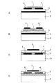
電界効果トランジスタ(FET)は、2つの電極(ソース、ドレイン)間の電気伝導度をゲート電極に印加する電圧で制御するものである。例えば、図1に示す構造を有する構造が挙げられる。ここで、1が有機半導体膜、2が絶縁体層、3と4がソースおよびドレイン電極、5がゲート電極、6が基板である。 A field effect transistor (FET) controls the electric conductivity between two electrodes (source and drain) by a voltage applied to a gate electrode. For example, a structure having the structure shown in FIG. Here, 1 is an organic semiconductor film, 2 is an insulator layer, 3 and 4 are source and drain electrodes, 5 is a gate electrode, and 6 is a substrate.
この半導体層を形成する際に、光照射による加熱処理をするのが本特許の主旨である。Bの構造のものを例に挙げると、基板6の上に、ゲート電極5を形成する。その際にゲート電極5は素子間の接続のためにパターニングされていることが必要である。その上に絶縁体層2を形成する。絶縁体層2の厚さは、下限が50nm以上であることが好ましく、特に100nm以上であることが好ましい。上限は5μm以下であることが好ましく、特に1μm以下であることが好ましい。さらに、その絶縁体層2上に有機半導体薄膜または前駆体薄膜を形成する。この薄膜にレーザで短時間照射して加熱することにより、有機半導体特性の改良あるいは有機半導体膜への変換を行う。一度の照射で不十分であれば、間隔をあけて何度も照射することができる。所望の半導体特性を示すようになった後で、ソースとドレイン電極(3、4)を形成する。このソース、ドレイン間の間隔は、下限が0.1μm以上であることが好ましく、特に1μm以上であることが好ましい。上限は500μm以下であることが好ましく、特に100μm以下であることが好ましい。この様な方法によってボトムゲート型の電界効果トランジスタ(FET)が得られる。
It is the gist of the present patent that heat treatment by light irradiation is performed when the semiconductor layer is formed. Taking the structure B as an example, the
なお、この例はボトムゲート型の素子であるが、他のトップゲート型等のタイプも同様に作製することができる。 Note that this example is a bottom gate type element, but other types such as a top gate type can be similarly manufactured.
本発明の電子デバイスの基板として用いられる材料は、上述した「A.積層体の製造方法」の欄で説明したものと同様であるので、ここでの説明は省略する。一方、各種電極を形成するための電極材料としては、白金、金、アルミニウム、クロム、ニッケル、銅、チタン、マグネシウム、カルシウム、バリウム、ナトリウム等の金属の他、酸化インジウムや酸化錫、あるいはその合金(ITO)、ポリアニリン、ポリピロール、ポリチオフェン、ポリアセチレン等の導電性高分子およびそれに塩酸、硫酸、スルホン酸等の酸、PF6、AsF5、FeCl3等のルイス酸、ヨウ素等のハロゲン原子、ナトリウムカリウム等の金属原子等のドーパントを添加したもの、金属粒子やカーボンブラック、フラーレン、カーボンナノチューブを分散した導電性の複合材料等の、導電性を有する材料が用いられる。また、半導体として用いられる自身の膜にドーピングして導電性を高めたものも用いることができる。 The materials used for the substrate of the electronic device of the present invention are the same as those described in the section of “A. On the other hand, electrode materials for forming various electrodes include metals such as platinum, gold, aluminum, chromium, nickel, copper, titanium, magnesium, calcium, barium, and sodium, as well as indium oxide, tin oxide, and alloys thereof. (ITO), conductive polymers such as polyaniline, polypyrrole, polythiophene and polyacetylene, and acids such as hydrochloric acid, sulfuric acid and sulfonic acid, Lewis acids such as PF 6 , AsF 5 and FeCl 3 , halogen atoms such as iodine and sodium potassium A material having conductivity such as a material to which a dopant such as a metal atom is added, a conductive composite material in which metal particles, carbon black, fullerene, and carbon nanotubes are dispersed is used. Further, a film obtained by doping a film used as a semiconductor to increase conductivity can be used.
また、絶縁体層に用いられる材料としては、ポリメチルメタクリレート、ポリスチレン、ポリビニルフェノール、ポリイミド、ポリカーボネート、ポリエステル、ポリビニルアルコール、ポリ酢酸ビニル、ポリウレタン、ポリスルホン、エポキシ樹脂、フェノール樹脂等の樹脂及びこれらを組み合わせた共重合体、二酸化珪素、酸化アルミニウム、酸化チタン等の酸化物、窒化珪素等の窒化膜、SrTiO3、BaTiO3等の強誘電性酸化物膜、あるいは、上記酸化物や窒化物、強誘電性酸化物等の粒子を分散させた樹脂膜等が挙げられる。一般に絶縁体層の静電容量が大きくなるほどゲート電圧を低電圧で駆動できることになるので、有利になる。これには、誘電率の大きな絶縁材料を用いるか、絶縁体層の厚さを薄くすることに対応する。絶縁体層は、塗布(スピンコーティングやブレードコーティング)、蒸着、スパッタ、スクリーン印刷やインクジェット等の印刷法、アルミ上のアルマイトの様に金属上に酸化膜を形成する方法等、材料特性に合わせた方法で作製することができる。 As the material used for the insulator layer, resins such as polymethyl methacrylate, polystyrene, polyvinyl phenol, polyimide, polycarbonate, polyester, polyvinyl alcohol, polyvinyl acetate, polyurethane, polysulfone, epoxy resin, and phenol resin, and a combination thereof Copolymers, oxides such as silicon dioxide, aluminum oxide, and titanium oxide; nitride films such as silicon nitride; ferroelectric oxide films such as SrTiO 3 and BaTiO 3; And a resin film in which particles such as a conductive oxide are dispersed. Generally, the larger the capacitance of the insulator layer, the lower the gate voltage can be driven, which is advantageous. This corresponds to using an insulating material having a large dielectric constant or reducing the thickness of the insulator layer. The insulator layer is adapted to the material characteristics, such as coating (spin coating or blade coating), evaporation, sputtering, printing methods such as screen printing and ink jet, and a method of forming an oxide film on metal like alumite on aluminum. It can be produced by a method.
本発明の電子デバイスは、これらの基板または絶縁体層の表面処理により特性を向上させることができる。これは基板の親水性/疎水性を調整して、製膜の際に得られる膜質を向上させること、特に基板あるいは絶縁体層と有機半導体膜の界面部分の特性を改良することがその原因と推定される。このような基板処理としては、ヘキサメチルジシラザン、シクロヘキセン、オクタデシルトリクロロシラン等の疎水化処理、塩酸や硫酸、酢酸等の酸や水酸化ナトリウム、水酸化カリウム、水酸化カルシウム、アンモニア等のアルカリ処理、オゾン処理、フッ素化処理、酸素やアルゴン等のプラズマ処理、ラングミュアブロジェット膜の形成処理、その他の絶縁体や半導体の薄膜の形成処理が挙げられる。 The characteristics of the electronic device of the present invention can be improved by surface treatment of the substrate or the insulator layer. This is because the hydrophilicity / hydrophobicity of the substrate is adjusted to improve the film quality obtained at the time of film formation, and in particular, the characteristics of the interface between the substrate or the insulator layer and the organic semiconductor film are improved. Presumed. Such substrate treatments include hydrophobizing treatments such as hexamethyldisilazane, cyclohexene, and octadecyltrichlorosilane, and acid treatments such as hydrochloric acid, sulfuric acid, and acetic acid, and alkali treatments such as sodium hydroxide, potassium hydroxide, calcium hydroxide, and ammonia. , Ozone treatment, fluorination treatment, plasma treatment with oxygen or argon, etc., formation of a Langmuir-Blodgett film, and other formation of an insulator or semiconductor thin film.
本発明の電子デバイスは、外気の影響を最小限にするために、保護膜を形成することができる。これには、エポキシ樹脂、アクリル樹脂、ポリウレタン、ポリイミド、ポリビニルアルコール等の樹脂膜、酸化珪素、窒化珪素、酸化アルミニウム等の無機酸化膜や窒化膜等が挙げられる。樹脂膜は、溶液の塗布乾燥する方法、モノマーを塗布あるいは蒸着して重合する方法が挙げられ、さらに架橋処理や多層膜を形成することも可能である。無機物の膜の形成には、スパッタ法、蒸着法等の真空プロセスでの形成方法や、ゾルゲル法に代表される溶液プロセスでの形成方法も用いることができる。 In the electronic device of the present invention, a protective film can be formed to minimize the influence of the outside air. This includes a resin film such as an epoxy resin, an acrylic resin, polyurethane, polyimide, and polyvinyl alcohol, and an inorganic oxide film and a nitride film such as silicon oxide, silicon nitride, and aluminum oxide. As the resin film, a method of applying and drying a solution, a method of applying or vapor-depositing a monomer and polymerizing the same, and a cross-linking treatment or forming a multilayer film can be used. For the formation of the inorganic film, a formation method by a vacuum process such as a sputtering method or an evaporation method, or a formation method by a solution process represented by a sol-gel method can be used.
本発明の電子デバイスは、ディスプレーのアクティブマトリクスのスイッチング素子として利用することができる。これは、ゲートに印加される電圧でソースとドレイン間の電流をスイッチングできることを利用して、ある表示素子に電圧を印加あるいは電流を供給する時のみスイッチを入れ、その他の時間は回路を切断する事により、高速、高コントラストな表示を行うものである。 The electronic device of the present invention can be used as an active matrix switching element of a display. This utilizes the fact that the current between the source and the drain can be switched by the voltage applied to the gate, so that the switch is turned on only when a voltage is applied or the current is supplied to a certain display element, and the circuit is disconnected at other times. Accordingly, high-speed, high-contrast display is performed.
適用される表示素子としては、液晶表示素子、高分子分散型液晶表示素子、電気泳動表示素子、エレクトロルミネッセント素子、エレクトロクロミック素子等が挙げられる。 Examples of the display element to be applied include a liquid crystal display element, a polymer dispersed liquid crystal display element, an electrophoretic display element, an electroluminescent element, an electrochromic element, and the like.
特に、本発明の有機電子デバイスは、低温プロセスでの素子作製が可能であり、プラスチック基板、プラスチックフィルムや紙等の、高温処理に耐えない基板を用いることができる。また、塗布あるいは印刷プロセスでの素子作製が可能であることから、大面積のディスプレーへの応用に適している。また、従来のアクティブマトリクスの代替としても、省エネルギープロセス、低コストプロセスの可能な素子として有利である。 In particular, the organic electronic device of the present invention can produce an element by a low-temperature process, and can use a substrate that does not withstand high-temperature treatment, such as a plastic substrate, a plastic film or paper. Further, since the element can be produced by a coating or printing process, it is suitable for application to a large-area display. It is also advantageous as an element that can be used as an energy-saving process and a low-cost process as a substitute for the conventional active matrix.
また、トランジスタを集積することにより、デジタル素子やアナログ素子が実現できる。これらの例としては、AND、OR、NAND、NOT等の論理回路、メモリー素子、発振素子、増幅素子等が挙げられる。さらにこれらを組み合わせることにより、ICカードやICタグを作製することができる。 Further, by integrating transistors, a digital element or an analog element can be realized. These examples include logic circuits such as AND, OR, NAND, and NOT, memory elements, oscillation elements, amplification elements, and the like. Further, by combining these, an IC card and an IC tag can be manufactured.
有機半導体は、ガスや化学物質、温度等の外部の刺激により、特性が大きく変化するので、それらのセンサーへの応用も考えられる。例えば、本発明の有機電子デバイスの特性が、気体や液体との接触により変化する量を測定することにより、定性的あるいは定量的にそれに含まれている化学物質を検出することが可能である。 The characteristics of organic semiconductors are greatly changed by external stimuli such as gases, chemical substances, and temperatures, and therefore, their application to sensors is also conceivable. For example, it is possible to qualitatively or quantitatively detect a chemical substance contained in the organic electronic device of the present invention by measuring an amount by which the characteristic of the organic electronic device changes by contact with a gas or a liquid.
なお、本発明は、上記実施形態に限定されるものではない。上記実施形態は、例示であり、本発明の特許請求の範囲に記載された技術的思想と実質的に同一な構成を有し、同様な作用効果を奏するものは、いかなるものであっても本発明の技術的範囲に包含される。 Note that the present invention is not limited to the above embodiment. The above-described embodiment is an exemplification, and has substantially the same configuration as the technical idea described in the claims of the present invention, and any device having the same operation and effect can be realized by the present invention. It is included in the technical scope of the invention.
以下に実施例を示して、本発明をさらに具体的に説明する。 Hereinafter, the present invention will be described more specifically with reference to examples.
(実施例1)
次に示すビシクロ化合物0.7wt%のクロロホルム溶液を、スライドグラス基板上にスピンコートすることにより、良好な100nm厚の膜を得た。CO2レーザ光(波長10.6μm、パワー2W、掃引速度1m/s、掃引ピッチ25μm、スポット径100μm、連続して光を照射する時間79μs)を照射して、この前駆体から有機半導体への変換を行った。吸収スペクトルでは690nm付近の吸収が現れていること、及びX線回折測定ではテトラベンゾポルフィリン由来のピークが現れていることから、上記前駆体から有機半導体への変換が起こっていることが分かった。図4に吸収スペクトル測定データを、図5にX線回折測定データを示す。
(Example 1)
A good 100 nm thick film was obtained by spin-coating a chloroform solution of the following bicyclo compound (0.7 wt%) on a slide glass substrate. CO 2 laser light (wavelength: 10.6 μm, power: 2 W, sweep speed: 1 m / s, sweep pitch: 25 μm, spot diameter: 100 μm, continuous light irradiation time: 79 μs) was irradiated to the organic semiconductor from the precursor. Conversion was performed. From the fact that absorption near 690 nm appeared in the absorption spectrum and the peak derived from tetrabenzoporphyrin appeared in the X-ray diffraction measurement, it was found that conversion from the precursor to the organic semiconductor had occurred. FIG. 4 shows the absorption spectrum measurement data, and FIG. 5 shows the X-ray diffraction measurement data.
(実施例2)
実施例1で用いたビシクロ化合物をゲート、ソース、ドレイン電極を設けた高ドープSi基板上にスピンコートし、良好な100nm厚の膜を得た。実施例1と同様のCO2レーザ光(但し、パワー12W、掃引速度3mm/s、連続して光を照射する時間27msに変更)を窒素雰囲気下で25μmピッチで照射して、前駆体から有機半導体への変換を行い、FET特性から飽和移動度を求めたところ、5×10−5cm2/Vsが得られた。
(Example 2)
The bicyclo compound used in Example 1 was spin-coated on a highly doped Si substrate provided with a gate, a source, and a drain electrode to obtain a good 100 nm thick film. The same CO 2 laser light as in Example 1 (however, the power was changed to 12 W, the sweep speed was 3 mm / s, and the continuous light irradiation time was changed to 27 ms) was irradiated at a pitch of 25 μm in a nitrogen atmosphere to convert the precursor into an organic compound. The conversion into a semiconductor was performed, and the saturation mobility was obtained from the FET characteristics. As a result, 5 × 10 −5 cm 2 / Vs was obtained.
(実施例3)
実施例1で用いたビシクロ化合物を80μm厚のポリイミド基板上にスピンコートし、良好な100nm厚の膜を得た。このポリイミド基板と実施例2で用いた高ドープSi基板とを、ビシクロ化合物と電極が接するように重ね、ポリイミド基板のビシクロ化合物を塗布していない側から、実施例1と同様のCO2レーザ(但し、パワー6W、掃引速度250mm/s、掃引ピッチ100μm、連続して光を照射する時間314μsに変更)を窒素雰囲気下で照射して、ポリイミド基板上のビシクロ化合物をSi基板上へ転写した。ポリイミド基板上の照射位置を変えて10回分の転写を重ね、FET特性から飽和移動度を求めたところ、1.4×10−4cm2/Vsが得られた。
(Example 3)
The bicyclo compound used in Example 1 was spin-coated on a polyimide substrate having a thickness of 80 μm to obtain a favorable film having a thickness of 100 nm. This polyimide substrate and the highly doped Si substrate used in Example 2 were overlapped so that the electrode was in contact with the bicyclo compound, and the same CO 2 laser as in Example 1 was used from the side of the polyimide substrate where the bicyclo compound was not applied. However, the power was changed to 6 W, the sweep speed was 250 mm / s, the sweep pitch was 100 μm, and the continuous light irradiation time was 314 μs) under a nitrogen atmosphere to transfer the bicyclo compound on the polyimide substrate onto the Si substrate. Transfer was repeated 10 times while changing the irradiation position on the polyimide substrate, and the saturation mobility was obtained from the FET characteristics. As a result, 1.4 × 10 −4 cm 2 / Vs was obtained.
(実施例4)
実施例1で用いたビシクロ化合物を300nmの熱酸化膜を設けた高ドープSi基板上に塗布し、良好な100nm厚の膜を得た。実施例1と同様のCO2レーザ(但し、パワー12W、掃引速度250mm/s、連続して光を照射する時間314μsに変更)を窒素雰囲気下で5回繰り返して照射して、前駆体から有機半導体への変換を行った。その上に、金のソース、ドレイン電極を作成し、FET特性から飽和移動度を求めたところ、2.7×10−3cm2/Vsが得られた。
(Example 4)
The bicyclo compound used in Example 1 was applied on a highly doped Si substrate provided with a 300 nm thermal oxide film to obtain a good 100 nm thick film. The same CO 2 laser as in Example 1 (however, the power was changed to 12 W, the sweep speed was changed to 250 mm / s, and the time for continuously irradiating light was changed to 314 μs) was repeated 5 times under a nitrogen atmosphere to irradiate the organic compound from the precursor. Conversion to semiconductor was performed. Gold source and drain electrodes were formed thereon, and the saturation mobility was determined from FET characteristics. As a result, 2.7 × 10 −3 cm 2 / Vs was obtained.
(実施例5)
実施例1で用いたビシクロ化合物2mgをクロロホルム1mLに溶解し、これをスライドグラス基板上にスピンコートすることにより良好な500nmの厚さの膜を得た。この膜の吸収スペクトルを測定すると、532nmでの吸光係数は2.4×10⁶(m−1)であった。
(Example 5)
2 mg of the bicyclo compound used in Example 1 was dissolved in 1 mL of chloroform, and this was spin-coated on a slide glass substrate to obtain a good film having a thickness of 500 nm. When the absorption spectrum of this film was measured, the extinction coefficient at 532 nm was 2.4 × 10 6 (m −1 ).
QスイッチパルスYAGレーザのSHG光(532nm、パルス幅10ns、連続して照射する時間10ns)を照射してこの前駆体から有機半導体への変換を行った。60mJ/パルスの光を5mmφのスポットで照射すると、照射した部分が緑色に変化し、その吸収スペクトルから上記前駆体から有機半導体への変換の起こっていることが分かった。
The precursor was converted to an organic semiconductor by irradiating SHG light (532 nm,
また、集光しない条件で、照射エネルギーを20mJ以下にすると変化は見られなかった。僅かに集光してレーザ光パワー密度を3倍に上げると照射した部分は白く抜けてしまった。したがって、ある照射パワーの範囲で前駆体から有機半導体に変換できる。 Further, no change was observed when the irradiation energy was set to 20 mJ or less under the condition that no light was collected. When the laser light power density was increased by a factor of three by slightly condensing, the irradiated part was lost in white. Therefore, a precursor can be converted into an organic semiconductor within a certain irradiation power range.
本手法で変換した有機半導体は、通常の加熱処理によって得られる膜と同等に良好な電気特性を示すと考えられる。 It is considered that the organic semiconductor converted by the present method shows good electric characteristics equivalent to a film obtained by a normal heat treatment.
(実施例6)
実施例5で用いたビシクロ化合物をPET基板上に成膜し、これを100rpmで回転させながら(回転半径15mm)、405nmの半導体レーザの光(パワー4mW)を1μmに集光して、連続して光を照射する時間5μsで照射したところ、基板には全く影響しないで照射した部分が緑色に変化していることから、上記前駆体から有機半導体への変換が起こっていると予想された。
(Example 6)
The bicyclo compound used in Example 5 was formed on a PET substrate, and while this was rotated at 100 rpm (rotation radius 15 mm), the light of a 405 nm semiconductor laser (
この有機半導体膜上にソース、ドレイン電極、絶縁体層、ゲート電極を形成したところ、電界効果トランジスタとして作動すると予想される。 When a source, drain electrode, insulator layer, and gate electrode are formed on this organic semiconductor film, it is expected that the organic semiconductor film will operate as a field effect transistor.
(実施例7)
実施例5で用いたビシクロ化合物をSi基板上に成膜し、これを100rpmで回転させながら(回転半径15mm)、405nmの半導体レーザの光(パワー4mW)を1μmに集光して、連続して光を照射する時間5μsで照射したところ、基板には全く影響しないで有機半導体膜のみが形成された。
(Example 7)
The bicyclo compound used in Example 5 was formed on a Si substrate, and while rotating it at 100 rpm (rotational radius 15 mm), the light of a 405 nm semiconductor laser (
(実施例8)
PET基板上にペンタセンを室温で蒸着し、成膜した。これにパルスYd:YAGレーザのSHG光(532nm、10ns、連続して光を照射する時間10ns)を照射して有機半導体膜を得た。得られた有機半導体膜の電気特性は、加熱処理して得られたものと同等であった。
(Example 8)
Pentacene was deposited on a PET substrate at room temperature to form a film. This was irradiated with pulsed Yd: YAG laser SHG light (532 nm, 10 ns, continuous
以上より、本発明の電子デバイスは、高特性を容易な作製プロセスで得ることができることが示された。 As described above, it was shown that the electronic device of the present invention can obtain high characteristics by an easy manufacturing process.
1 … 有機半導体膜
2 … 絶縁体層
3 … ソース電極
4 … ドレイン電極
5 … ゲート電極
6 … 基板
10 … 有機半導体薄膜またはその前駆体薄膜
11 … 基板
12 … 有機半導体膜
13 … 基板
21 … 活性エネルギー線
DESCRIPTION OF
Claims (7)
The electronic device according to claim 6, wherein the organic electronic device is a field effect transistor.
Priority Applications (1)
| Application Number | Priority Date | Filing Date | Title |
|---|---|---|---|
| JP2004011131A JP2004247716A (en) | 2003-01-23 | 2004-01-19 | Method for manufacturing laminated body |
Applications Claiming Priority (2)
| Application Number | Priority Date | Filing Date | Title |
|---|---|---|---|
| JP2003015053 | 2003-01-23 | ||
| JP2004011131A JP2004247716A (en) | 2003-01-23 | 2004-01-19 | Method for manufacturing laminated body |
Publications (2)
| Publication Number | Publication Date |
|---|---|
| JP2004247716A true JP2004247716A (en) | 2004-09-02 |
| JP2004247716A5 JP2004247716A5 (en) | 2007-03-01 |
Family
ID=33032032
Family Applications (1)
| Application Number | Title | Priority Date | Filing Date |
|---|---|---|---|
| JP2004011131A Pending JP2004247716A (en) | 2003-01-23 | 2004-01-19 | Method for manufacturing laminated body |
Country Status (1)
| Country | Link |
|---|---|
| JP (1) | JP2004247716A (en) |
Cited By (19)
| Publication number | Priority date | Publication date | Assignee | Title |
|---|---|---|---|---|
| JP2006131509A (en) * | 2004-11-02 | 2006-05-25 | Sharp Corp | Method for producing silanized pentacene precursor and organic thin film by using the same |
| JP2006245559A (en) * | 2005-02-07 | 2006-09-14 | Mitsubishi Chemicals Corp | Field-effect transistor and manufacturing method thereof |
| JP2006352143A (en) * | 2005-06-18 | 2006-12-28 | Samsung Sdi Co Ltd | Patterning method of organic semiconductor |
| JP2007115927A (en) * | 2005-10-20 | 2007-05-10 | Tokyo Univ Of Agriculture & Technology | Heat treatment method |
| JP2007273938A (en) * | 2005-09-06 | 2007-10-18 | Canon Inc | Method of manufacturing semiconductor device |
| JP2008515654A (en) * | 2004-10-12 | 2008-05-15 | ナノシス・インク. | Fully integrated organic layer process for manufacturing plastic electronic components based on conducting polymers and semiconductor nanowires |
| JPWO2006054686A1 (en) * | 2004-11-18 | 2008-06-05 | コニカミノルタホールディングス株式会社 | Organic thin film transistor manufacturing method and organic thin film transistor |
| JP2008524869A (en) * | 2004-12-21 | 2008-07-10 | イーストマン コダック カンパニー | N-type semiconductor material for thin film transistor |
| JP2008524846A (en) * | 2004-12-17 | 2008-07-10 | イーストマン コダック カンパニー | N-type semiconductor material for thin film transistor |
| JP2008544519A (en) * | 2005-06-14 | 2008-12-04 | シン フイルム エレクトロニクス エイエスエイ | Method for manufacturing ferroelectric memory device |
| WO2009081796A1 (en) * | 2007-12-20 | 2009-07-02 | Konica Minolta Holdings, Inc. | Electronic device and method for manufacturing electronic device |
| JP2010140654A (en) * | 2008-12-09 | 2010-06-24 | Hitachi Zosen Corp | Manufacturing method of transparent conductive film |
| CN101847661A (en) * | 2009-03-26 | 2010-09-29 | 株式会社半导体能源研究所 | Semiconductor device and method for manufacturing the same |
| WO2012141116A1 (en) * | 2011-04-11 | 2012-10-18 | 昭和電工株式会社 | Organic semiconductor material activation method |
| GB2492442A (en) * | 2011-06-27 | 2013-01-02 | Pragmatic Printing Ltd | Method of manufacturing a thin film transistor |
| GB2492532A (en) * | 2011-06-27 | 2013-01-09 | Pragmatic Printing Ltd | Method of manufacturing a thin film transistor |
| WO2014141846A1 (en) * | 2013-03-13 | 2014-09-18 | 富士フイルム株式会社 | Method for forming organic semiconductor film |
| JP2015070082A (en) * | 2013-09-27 | 2015-04-13 | 富士フイルム株式会社 | Method of producing metal oxide film, metal oxide film, thin film transistor, display, image sensor and x-ray sensor |
| US9711725B2 (en) | 2013-03-19 | 2017-07-18 | Fujifilm Corporation | Method for producing organic semiconductor element |
Citations (4)
| Publication number | Priority date | Publication date | Assignee | Title |
|---|---|---|---|---|
| JPH04199638A (en) * | 1990-11-29 | 1992-07-20 | Ricoh Co Ltd | Field effect transistor, display device using the same and manufacture thereof |
| JPH0697523A (en) * | 1992-09-10 | 1994-04-08 | Nec Corp | Treatment of molecular material |
| JP2002324931A (en) * | 2001-03-30 | 2002-11-08 | Lucent Technol Inc | Method for manufacturing integrated circuit tin film transistor device |
| WO2002095805A2 (en) * | 2001-05-23 | 2002-11-28 | Plastic Logic Limited | Laser parrering of devices |
-
2004
- 2004-01-19 JP JP2004011131A patent/JP2004247716A/en active Pending
Patent Citations (4)
| Publication number | Priority date | Publication date | Assignee | Title |
|---|---|---|---|---|
| JPH04199638A (en) * | 1990-11-29 | 1992-07-20 | Ricoh Co Ltd | Field effect transistor, display device using the same and manufacture thereof |
| JPH0697523A (en) * | 1992-09-10 | 1994-04-08 | Nec Corp | Treatment of molecular material |
| JP2002324931A (en) * | 2001-03-30 | 2002-11-08 | Lucent Technol Inc | Method for manufacturing integrated circuit tin film transistor device |
| WO2002095805A2 (en) * | 2001-05-23 | 2002-11-28 | Plastic Logic Limited | Laser parrering of devices |
Cited By (29)
| Publication number | Priority date | Publication date | Assignee | Title |
|---|---|---|---|---|
| JP2008515654A (en) * | 2004-10-12 | 2008-05-15 | ナノシス・インク. | Fully integrated organic layer process for manufacturing plastic electronic components based on conducting polymers and semiconductor nanowires |
| JP2006131509A (en) * | 2004-11-02 | 2006-05-25 | Sharp Corp | Method for producing silanized pentacene precursor and organic thin film by using the same |
| JPWO2006054686A1 (en) * | 2004-11-18 | 2008-06-05 | コニカミノルタホールディングス株式会社 | Organic thin film transistor manufacturing method and organic thin film transistor |
| JP2008524846A (en) * | 2004-12-17 | 2008-07-10 | イーストマン コダック カンパニー | N-type semiconductor material for thin film transistor |
| JP2008524869A (en) * | 2004-12-21 | 2008-07-10 | イーストマン コダック カンパニー | N-type semiconductor material for thin film transistor |
| JP2006245559A (en) * | 2005-02-07 | 2006-09-14 | Mitsubishi Chemicals Corp | Field-effect transistor and manufacturing method thereof |
| JP2008544519A (en) * | 2005-06-14 | 2008-12-04 | シン フイルム エレクトロニクス エイエスエイ | Method for manufacturing ferroelectric memory device |
| JP2006352143A (en) * | 2005-06-18 | 2006-12-28 | Samsung Sdi Co Ltd | Patterning method of organic semiconductor |
| JP2007273938A (en) * | 2005-09-06 | 2007-10-18 | Canon Inc | Method of manufacturing semiconductor device |
| JP2007115927A (en) * | 2005-10-20 | 2007-05-10 | Tokyo Univ Of Agriculture & Technology | Heat treatment method |
| JP5423396B2 (en) * | 2007-12-20 | 2014-02-19 | コニカミノルタ株式会社 | Electronic device and method for manufacturing electronic device |
| WO2009081796A1 (en) * | 2007-12-20 | 2009-07-02 | Konica Minolta Holdings, Inc. | Electronic device and method for manufacturing electronic device |
| JP2010140654A (en) * | 2008-12-09 | 2010-06-24 | Hitachi Zosen Corp | Manufacturing method of transparent conductive film |
| CN101847661A (en) * | 2009-03-26 | 2010-09-29 | 株式会社半导体能源研究所 | Semiconductor device and method for manufacturing the same |
| WO2012141116A1 (en) * | 2011-04-11 | 2012-10-18 | 昭和電工株式会社 | Organic semiconductor material activation method |
| GB2492442A (en) * | 2011-06-27 | 2013-01-02 | Pragmatic Printing Ltd | Method of manufacturing a thin film transistor |
| US9425193B2 (en) | 2011-06-27 | 2016-08-23 | Pragmatic Printing Ltd | Methods of manufacturing transistors including forming a depression in a surface of a covering of resist material |
| US10672765B2 (en) | 2011-06-27 | 2020-06-02 | National Centre For Printable Electronics | Methods of manufacturing transistors including forming a depression in a surface of a covering of resist material |
| GB2492532A (en) * | 2011-06-27 | 2013-01-09 | Pragmatic Printing Ltd | Method of manufacturing a thin film transistor |
| GB2522565B (en) * | 2011-06-27 | 2016-02-03 | Pragmatic Printing Ltd | Transistor and its method of manufacture |
| GB2492532B (en) * | 2011-06-27 | 2015-06-03 | Pragmatic Printing Ltd | Transistor and its method of manufacture |
| GB2522565A (en) * | 2011-06-27 | 2015-07-29 | Pragmatic Printing Ltd | Transistor and its method of manufacture |
| GB2492442B (en) * | 2011-06-27 | 2015-11-04 | Pragmatic Printing Ltd | Transistor and its method of manufacture |
| US20150364686A1 (en) * | 2013-03-13 | 2015-12-17 | Fujifilm Corporation | Method for forming organic semiconductor film |
| JP2014179371A (en) * | 2013-03-13 | 2014-09-25 | Fujifilm Corp | Method for forming organic semiconductor film |
| US9680099B2 (en) | 2013-03-13 | 2017-06-13 | Fujifilm Corporation | Method for forming organic semiconductor film |
| WO2014141846A1 (en) * | 2013-03-13 | 2014-09-18 | 富士フイルム株式会社 | Method for forming organic semiconductor film |
| US9711725B2 (en) | 2013-03-19 | 2017-07-18 | Fujifilm Corporation | Method for producing organic semiconductor element |
| JP2015070082A (en) * | 2013-09-27 | 2015-04-13 | 富士フイルム株式会社 | Method of producing metal oxide film, metal oxide film, thin film transistor, display, image sensor and x-ray sensor |
Similar Documents
| Publication | Publication Date | Title |
|---|---|---|
| JP2004247716A (en) | Method for manufacturing laminated body | |
| KR101192615B1 (en) | Field effect transistor | |
| Kwak et al. | Tailoring Morphology and Structure of Inkjet‐Printed Liquid‐Crystalline Semiconductor/Insulating Polymer Blends for High‐Stability Organic Transistors | |
| JP2007019014A (en) | Flat panel display device and its manufacturing method | |
| JP4977968B2 (en) | Manufacturing method of electronic device | |
| JP2003304014A (en) | Organic electronic device and its manufacturing method | |
| US8883546B2 (en) | Process for preparing an organic electronic device | |
| JP4572501B2 (en) | Method for producing organic thin film transistor | |
| JP5137296B2 (en) | Field effect transistor | |
| JP2005072569A (en) | Organic fet | |
| WO2016088793A1 (en) | Organic compound and uses thereof | |
| JP6592758B2 (en) | Novel condensed polycyclic aromatic compounds and uses thereof | |
| JP2003309268A (en) | Organic transistor element and manufacturing method therefor | |
| JP2017521395A (en) | N-fluoroalkyl substituted dibromonaphthalenediimides and their use as semiconductors | |
| JP2008226959A (en) | Organic field-effect transistor and manufacturing method therefor | |
| Yamazaki et al. | Drastic improvement in wettability of 6, 13-bis (triisopropylsilylethynyl) pentacene by addition of silica nanoparticles for solution-processable organic field-effect transistors | |
| Makrygianni et al. | Laser printed organic semiconductor PQT-12 for bottom-gate organic thin-film transistors: Fabrication and characterization | |
| KR101172187B1 (en) | Fabrication of thin film transistor and integrated circuits by spray printing method | |
| JP2005322895A (en) | Organic electronic-device and manufacturing method thereof | |
| JP5023630B2 (en) | Method for manufacturing organic semiconductor element | |
| KR101101479B1 (en) | Improvement of charge injection in organic thin film transistor by local doping | |
| JP4281324B2 (en) | ORGANIC THIN FILM TRANSISTOR DEVICE, ITS MANUFACTURING METHOD, AND ORGANIC THIN FILM TRANSISTOR SHEET | |
| JP2004228371A (en) | Field effect transistor | |
| JP4696700B2 (en) | Organic semiconductor thin film manufacturing method, organic electronic device manufacturing method, and organic field effect transistor manufacturing method | |
| Yasuda et al. | Fabrication of stretch-oriented regioregular poly (3-hexylthiophene) film and its application to organic field-effect transistors |
Legal Events
| Date | Code | Title | Description |
|---|---|---|---|
| A521 | Request for written amendment filed |
Free format text: JAPANESE INTERMEDIATE CODE: A523 Effective date: 20070116 |
|
| A621 | Written request for application examination |
Free format text: JAPANESE INTERMEDIATE CODE: A621 Effective date: 20070116 |
|
| A131 | Notification of reasons for refusal |
Free format text: JAPANESE INTERMEDIATE CODE: A131 Effective date: 20110201 |
|
| A02 | Decision of refusal |
Free format text: JAPANESE INTERMEDIATE CODE: A02 Effective date: 20110705 |