JP2004239834A - Defect detecting apparatus and defect detection method for hologram - Google Patents
Defect detecting apparatus and defect detection method for hologram Download PDFInfo
- Publication number
- JP2004239834A JP2004239834A JP2003031134A JP2003031134A JP2004239834A JP 2004239834 A JP2004239834 A JP 2004239834A JP 2003031134 A JP2003031134 A JP 2003031134A JP 2003031134 A JP2003031134 A JP 2003031134A JP 2004239834 A JP2004239834 A JP 2004239834A
- Authority
- JP
- Japan
- Prior art keywords
- hologram
- light
- image data
- inspection
- diffracted light
- Prior art date
- Legal status (The legal status is an assumption and is not a legal conclusion. Google has not performed a legal analysis and makes no representation as to the accuracy of the status listed.)
- Pending
Links
Images


Landscapes
- Investigating Materials By The Use Of Optical Means Adapted For Particular Applications (AREA)
- Testing Of Optical Devices Or Fibers (AREA)
- Holo Graphy (AREA)
Abstract
Description
【0001】
【発明の属する技術分野】
本発明は、ホログラムの欠陥、特に回折格子自体の不良や欠陥を検出する欠陥検出装置および欠陥検出方法に関する。
【0002】
【従来の技術】
通常、転写型ホログラムは、レリーフ状の回折格子を平面上に記録したスタンパを、例えば樹脂表面に押しつけることによって回折格子パターンを樹脂表面に転写した後に、表面に金属が蒸着され、反射層が形成されることによって製造されている。もちろん、樹脂以外の種々の材料が使われることもある。
【0003】
このようにして製造されたホログラムのデザインは多種多様であり、回折方向は様々で任意の方向を取る。これにより、ホログラムは、光が入射する角度によって様々なパターンの画像を再生することができることから、ICカードや、クレジットカードに貼り付けることによって、偽造防止や、セキュリティ管理等に応用がなされている。このようにホログラムは、偽造防止や、セキュリティ管理等に応用されていることから、確実に製作することが要求される。
【0004】
しかしながら、上述したようなホログラムは、ミクロンオーダでかつ非常に複雑な回折格子のパターンによって精密に形成されるものであるので、その製造は容易ではなく、製造段階においても十分に注意を払う必要がある。
【0005】
例えば、スタンパにゴミ等の異物が付着し、異物が付いたままの状態でホログラムが製造されると、スタンパを押すたび毎に回折格子の凹凸が潰れてしまい、表面に正しい回折格子パターンが得られなくなる。したがって、製造後においても、欠陥がないかどうかを厳重に検査する必要がある。
【0006】
【発明が解決しようとする課題】
しかしながら、ホログラムの欠陥を検出することは、以下に示すように容易ではない。
【0007】
すなわち、通常、ホログラムは、回折光を見ることになるので、視点によって像の見え方が変化する。このため、直接反射光や、単一もしくは複数の光源を用いた照明条件下では、一度に全画像を見ることはできない。また、光の照射条件の僅かな違いによっても見える画像が変化する。したがって、検査しようとする画像が安定せず、検査結果も信頼性が保てない。
【0008】
したがって、実際には、ホログラムの品種に応じて角度が固定された光照射系と撮像系からなる検査装置を用いて検査する方法が一番現実的、かつ、容易とされている。
【0009】
しかしながら、検査対象とするホログラムの品種を変更する毎に光照射系と撮像系とを調節してから検査すること自体容易な作業ではなく、手間と時間とを要する。また、ホログラムのとる回折角度によっては、検査装置の構造上回折光を取れず、部分的な検査しかできない場合もある。
【0010】
このような事情のため、任意の品種のホログラムを自動的に検査することは、到底現実的ではなく、ホログラムの品質は一部、あるいは大部分を目視チェックに頼らざるを得ない。
【0011】
このため、万が一表面に正しい回折格子が形成されず、欠陥のあるホログラムが製造されても、その欠陥を検出することは困難であり、欠陥のあるホログラムが連続して多数製造され続ける可能性があるという問題がある。
【0012】
本発明はこのような事情に鑑みてなされたものであり、任意の品種のホログラムの欠陥検出に、汎用的に利用することができ、かつ欠陥を精度良く検出することが可能なホログラムの欠陥検出装置および欠陥検出方法を提供することを目的とする。
【0013】
【課題を解決するための手段】
上記の目的を達成するために、本発明では、以下のような手段を講じる。
【0014】
すなわち、請求項1の発明は、ホログラムの欠陥を検出する装置であって、ホログラムの表面に対する法線方向を除く実質的な表面側全方向から検査光を照射する検査光用光源と、検査光がホログラムによって反射されてなる反射光から、検査光がホログラムによって回折されてなる回折光を抽出する回折光抽出手段と、回折光抽出手段によって抽出された回折光を撮像し、画像データを取得する撮像手段と、撮像手段によって取得された画像データと、予め撮像された基準画像データとに基づいて、ホログラムに欠陥が有るか否かを判定する判定手段とを備えている。
【0015】
従って、請求項1の発明のホログラムの欠陥検出装置においては、以上のような手段を講じることにより、ホログラムの表面に欠陥がある場合には、検査光は法線方向には回折しないので、法線方向から見た画像データの中には、欠陥のある部分が黒い点として撮像される。
【0016】
したがって、この黒い点が観察された場合には、ホログラムの表面には欠陥があるものと判定することにより、ホログラムの表面の欠陥を精度良く検出することが可能となる。
【0017】
請求項2の発明は、請求項1の発明のホログラムの欠陥検出装置において、回折光抽出手段は、反射光のうち、法線方向に沿って進む光を回折光として抽出するようにしている。
【0018】
従って、請求項2の発明のホログラムの欠陥検出装置においては、以上のような手段を講じることにより、回折光抽出手段は、反射光のうち、法線方向に沿って進む光のみを回折光として抽出することができる。これによって、ホログラムの欠陥検出精度を高めることができる。
【0019】
請求項3の発明は、ホログラムの欠陥を検出する装置であって、ホログラムの表面に対する法線方向を除く実質的な表面側全方向から検査光を照射する検査光用光源と、検査光がホログラムを透過してなる透過光から、検査光がホログラムによって回折されてなる回折光を抽出する回折光抽出手段と、回折光抽出手段によって抽出された回折光を撮像し、画像データを取得する撮像手段と、撮像手段によって取得された画像データと、予め撮像された基準画像データとに基づいて、ホログラムに欠陥が有るか否かを判定する判定手段とを備えている。
【0020】
従って、請求項3の発明のホログラムの欠陥検出装置においては、以上のような手段を講じることにより、撮像された回折光の画像データを、予め撮影されている正常なホログラムの画像データと比較することによって、精度良く欠陥を検出することができる。
【0021】
請求項4の発明は、請求項3の発明のホログラムの欠陥検出装置において、回折光抽出手段は、透過光のうち、法線方向へ沿って進む光を回折光として抽出するようにしている。
【0022】
従って、請求項4の発明のホログラムの欠陥検出装置においては、以上のような手段を講じることにより、回折光抽出手段は、透過光のうち、法線方向に沿って進む光のみを回折光として抽出することができる。これによって、ホログラムの欠陥検出精度を高めることができる。
【0023】
請求項5の発明は、請求項2または請求項4の発明のホログラムの欠陥検出装置において、撮像手段とホログラムとの間に備えられ、法線方向へ沿って進む光を撮像手段に導くテレセントリックレンズを、回折光抽出手段として用いている。
【0024】
テレセントリックレンズは、検査光によって照射された該ホログラムからの回折光のうち法線方向に沿って進む光のみを捉える。従って、請求項5の発明のホログラムの欠陥検出装置においては、以上のような手段を講じることにより、ホログラムの表面に欠陥がある場合には、法線方向から見た画像データ中に黒い点として撮像することができる。その結果、ホログラムの表面の欠陥を精度良く検出することが可能となる。
【0025】
請求項6の発明は、請求項1乃至5のうち何れか1項の発明のホログラムの欠陥検出装置において、ホログラムによって回折されてなる回折光のうち、法線方向に沿って進み、かつ撮像手段によって撮像可能な波長領域の回折光を得ることができるような検査光のホログラムに対する照射角度範囲よりも、法線方向側に回折光抽出手段を配置するようにしている。
【0026】
従って、請求項6の発明のホログラムの欠陥検出装置においては、以上のような手段を講じることにより、検査光が回折光抽出手段によって干渉されることなく、ホログラムに対して実質的な表面側全方向から検査光を照射することができる。これによって、ホログラムの表面全域に亘って、死角なく欠陥検査を行うことができる。なお、撮像手段によって撮像可能な波長領域の回折光を得ることができるような検査光のホログラムに対する照射角度範囲とは、図5のK、Lの領域を指している。
【0027】
請求項7の発明は、請求項1乃至6のうち何れか1項の発明のホログラムの欠陥検出装置において、ホログラムによって回折されてなる回折光のうち、法線方向に沿って進み、かつ撮像手段によって撮像可能な波長領域の回折光を得ることができるような検査光のホログラムに対する照射角度範囲よりも、ホログラムの表面を含む面側から検査光を照射できるように検査光用光源を配置するとともに、ホログラムを検査光用光源から見て凸状になるように丸めるローラを付加している。そして、ローラによってホログラムを丸めた状態で検査光用光源から検査光を照射することによって、ホログラムの表面の任意場所に対して、照射角度範囲における任意の照射角度で検査光を照射するようにしている。
【0028】
従って、請求項7の発明のホログラムの欠陥検出装置においては、以上のような手段を講じることにより、ホログラムの表面全領域に対して、真横の角度からであっても検査光を照射することができる。これによって、ホログラムの表面全域に亘って、死角なく欠陥検査を行うことができる。
【0029】
請求項8の発明は、請求項1乃至7のうち何れか1項の発明のホログラムの欠陥検出装置において、ホログラムの近傍に回折方向および回折ピッチが予め把握されたホログラムマークを配置している。そして、検査光用光源は、ホログラムの表面とホログラムマークの表面とを含んだ領域に対して検査光を照射し、回折光抽出手段は、検査光が領域によって反射されてなる反射光から、検査光がホログラムおよびホログラムマークによって回折されてなる回折光を抽出し、撮像手段は、この抽出された回折光を撮像することによって画像データを取得する。更に、判定手段は、この取得された画像データのうちのホログラムに該当する部分とホログラムマークに該当する部分との光強度を比較し、比較結果に基づいてホログラムに欠陥が有るか否かを判定するようにしている。
【0030】
従って、請求項8の発明のホログラムの欠陥検出装置においては、以上のような手段を講じることにより、検査対象とするホログラムの画像データを、ホログラムマークの画像データを基準として比較することによって、検査対象とするホログラムの欠陥検査を行うことが可能となる。
【0031】
請求項9の発明は、請求項1乃至7のうち何れか1項の発明のホログラムの欠陥検出装置において、ホログラムとの相対位置、形状、回折方向および回折ピッチが予め把握されたホログラムマークを配置している。そして、検査光用光源は、ホログラムマークの表面に対して検査光を照射し、回折光抽出手段は、検査光がホログラムマークによって反射されてなる反射光から、検査光がホログラムマークによって回折されてなる回折光を抽出する。更に、撮像手段は、この抽出された回折光を撮像することによって画像データを取得し、判定手段は、この取得された画像データに基づいて、ホログラムの位置を把握する。
【0032】
従って、請求項9の発明のホログラムの欠陥検出装置においては、以上のような手段を講じることにより、例えばフィルム上に連続的に製造されたホログラムに対しても、ホログラムマークの位置を参照しながら検査することによって、撮像手段により得られたホログラム画像を正しい位置に配置しながら、ホログラムの欠陥検査を行うことが可能となる。
【0033】
請求項10の発明は、請求項1乃至9のうち何れか1項の発明のホログラムの欠陥検出装置において、判定手段は、予め撮像された基準画像データから得られる基準画像輝度分布と、撮像手段によって取得された画像データから得られる検査画像輝度分布とを比較し、検査画像輝度分布において基準画像輝度分布に対して暗輝度側に突出しているピークに対応する位置に欠陥があるものと判定するようにしている。
【0034】
ホログラムに欠陥がある場合、ホログラム表面に対する法線方向への回折光は存在しないので、法線方向に沿って進む回折光を撮影すると、その画像データには欠陥のある場所が黒い点として撮影される。すなわち、この画像データに基づく輝度分布において、この黒い点は、欠陥のないホログラムの画像データに基づく輝度分布に対して暗輝度側に突出したピークとして検出される。したがって、請求項10の発明のホログラムの欠陥検出装置は、この暗輝度側のピークを検出することによって、対応する場所に欠陥があるものと判定することができる。
【0035】
請求項11の発明は、ホログラムの欠陥を検出する方法であって、ホログラムの表面に対する法線方向を除く実質的な表面側全方向から検査光を照射し、検査光がホログラムによって反射されてなる反射光から、検査光がホログラムによって回折されてなる回折光を回折光抽出手段によって抽出する。そして、抽出された回折光を撮像手段によって撮像することによって画像データを取得し、取得された画像データと、予め撮像された基準画像データとに基づいて、ホログラムに欠陥が有るか否かを判定するようにしている。
【0036】
従って、請求項11の発明のホログラムの欠陥検出方法においては、以上のような手段を講じることにより、ホログラムの表面に欠陥がある場合には、検査光は法線方向には回折しないので、法線方向から見た画像データの中には、欠陥のある場所が黒い点として撮像される。
【0037】
したがって、この黒い点が観察された場合には、ホログラムの表面には欠陥があるものと判定することにより、ホログラムの表面の欠陥を精度良く検出することが可能となる。
【0038】
請求項12の発明は、請求項11の発明のホログラムの欠陥検出方法において、回折光抽出手段は、検査光がホログラムによって反射されてなる反射光のうち、法線方向に沿って進む光を回折光として抽出するようにしている。
【0039】
従って、請求項12の発明のホログラムの欠陥検出方法においては、以上のような手段を講じることにより、回折光抽出手段は、反射光のうち、法線方向に沿って進む光のみを回折光として抽出することができる。これによって、ホログラムの欠陥検出精度を高めることができる。
【0040】
請求項13の発明は、ホログラムの欠陥を検出する方法であって、ホログラムの表面に対する法線方向を除く実質的な表面側全方向から検査光を照射し、検査光がホログラムを透過してなる透過光から、検査光がホログラムによって回折されてなる回折光を回折光抽出手段によって抽出する。そして、抽出された回折光を撮像手段によって撮像することによって画像データを取得し、取得された画像データと、予め撮像された基準画像データとに基づいて、ホログラムに欠陥が有るか否かを判定するようにしている。
【0041】
従って、請求項13の発明のホログラムの欠陥検出方法においては、以上のような手段を講じることにより、撮像された回折光の画像データを、予め撮影されている正常なホログラムの画像データと比較することによって、精度良く欠陥を検出することができる。
【0042】
請求項14の発明は、請求項13の発明のホログラムの欠陥検出方法において、回折光抽出手段は、検査光がホログラムを透過してなる透過光のうち、法線方向へ沿って進む光を回折光として抽出するようにしている。
【0043】
従って、請求項14の発明のホログラムの欠陥検出方法においては、以上のような手段を講じることにより、回折光抽出手段は、透過光のうち、法線方向に沿って進む光のみを回折光として抽出することができる。これによって、ホログラムの欠陥検出精度を高めることができる。
【0044】
請求項15の発明は、請求項12または請求項14の発明のホログラムの欠陥検出方法において、回折光抽出手段として、撮像手段とホログラムとの間に配置されたテレセントリックレンズを用いている。
【0045】
テレセントリックレンズは、検査光によって照射された該ホログラムからの回折光のうち法線方向に沿って進む光のみを捉える。従って、請求項15の発明のホログラムの欠陥検出方法においては、以上のような手段を講じることにより、ホログラムの表面に欠陥がある場合には、法線方向から見た画像データ中に黒い点として撮像することができる。その結果、ホログラムの表面の欠陥を精度良く検出することが可能となる。
【0046】
請求項16の発明は、請求項11乃至15のうち何れか1項の発明のホログラムの欠陥検出方法において、ホログラムによって回折されてなる回折光のうち、法線方向に沿って進み、かつ撮像手段によって撮像可能な波長領域の回折光を得ることができるような検査光のホログラムに対する照射角度範囲よりも、法線方向側に回折光抽出手段を配置するようにしている。
【0047】
従って、請求項16の発明のホログラムの欠陥検出方法においては、以上のような手段を講じることにより、検査光が回折光抽出手段によって干渉されることなく、ホログラムに対して実質的な表面側全方向から検査光を照射することができる。これによって、ホログラムの表面全域に亘って、死角なく欠陥検査を行うことができる。
【0048】
請求項17の発明は、請求項11乃至16のうち何れか1項の発明のホログラムの欠陥検出方法において、ホログラムによって回折されてなる回折光のうち、法線方向に沿って進み、かつ撮像手段によって撮像可能な波長領域の回折光を得ることができるような検査光のホログラムに対する照射角度範囲よりも、ホログラムの表面を含む面側から検査光を照射するとともに、ホログラムを検査光を照射する側から見て凸状になるように丸めた状態で検査光を照射することによって、ホログラムの表面の任意場所に対して、照射角度範囲における任意の照射角度で検査光を照射するようにしている。
【0049】
従って、請求項17の発明のホログラムの欠陥検出方法においては、以上のような手段を講じることにより、ホログラム表面の全領域に対して、真横の角度からであっても検査光を照射することができる。これによって、ホログラムの表面全域に亘って、死角なく欠陥検査を行うことができる。
【0050】
請求項18の発明は、請求項11乃至17のうち何れか1項の発明のホログラムの欠陥検出方法において、ホログラムの近傍に回折方向および回折ピッチが予め把握されたホログラムマークを配置し、ホログラムの表面とホログラムマークの表面とを含んだ領域に対して検査光を照射し、検査光が領域によって反射されてなる反射光から、検査光がホログラムおよびホログラムマークによって回折されてなる回折光を回折光抽出手段によって抽出する。そして、この抽出された回折光を撮像手段が撮像することによって画像データを取得し、この取得された画像データのうちのホログラムに該当する部分とホログラムマークに該当する部分との光強度を比較し、比較結果に基づいてホログラムに欠陥が有るか否かを判定するようにしている。
【0051】
従って、請求項18の発明のホログラムの欠陥検出方法においては、以上のような手段を講じることにより、検査対象とするホログラムの画像データを、ホログラムマークの画像データを基準として比較することによって、検査対象とするホログラムの欠陥検査を行うことが可能となる。
【0052】
請求項19の発明は、請求項11乃至17のうち何れか1項の発明のホログラムの欠陥検出方法において、ホログラムとの相対位置、形状、回折方向および回折ピッチが予め把握されたホログラムマークを配置し、ホログラムマークの表面に対して検査光を照射し、検査光がホログラムマークによって反射されてなる反射光から、検査光がホログラムマークによって回折されてなる回折光を回折光抽出手段によって抽出する。そして、この抽出された回折光を撮像手段が撮像することによって画像データを取得し、この取得された画像データに基づいて、ホログラムの位置を把握するようにしている。
【0053】
従って、請求項19の発明のホログラムの欠陥検出方法においては、以上のような手段を講じることにより、例えばフィルム上に連続的に製造されたホログラムに対しても、ホログラムマークの位置を参照しながら検査することによって、撮像手段により得られたホログラム画像を正しい位置に配置しながら、ホログラムの欠陥検査を行うことが可能となる。
【0054】
請求項20の発明は、請求項11乃至19のうち何れか1項の発明のホログラムの欠陥検出方法において、予め撮像された基準画像データから得られる基準画像輝度分布と、撮像手段によって取得された画像データから得られる検査画像輝度分布とを比較し、検査画像輝度分布において基準画像輝度分布に対して暗輝度側に突出しているピークに対応する位置に欠陥があるものと判定するようにしている。
【0055】
ホログラムに欠陥がある場合、ホログラム表面に対する法線方向への回折光は存在しないので、法線方向に沿って進む回折光を撮影すると、その画像データには欠陥のある場所が黒い点として撮影される。すなわち、この画像データに基づく輝度分布において、この黒い点は、欠陥のないホログラムの画像データに基づく輝度分布に対して暗輝度側に突出したピークとして検出される。したがって、請求項20の発明のホログラムの欠陥検出方法では、この暗輝度側のピークを検出することによって、対応する場所に欠陥があるものと判定することができる。
【0056】
【発明の実施の形態】
以下に、本発明の各実施の形態について図面を参照しながら説明する。
【0057】
(第1の実施の形態)
本発明の第1の実施の形態を図1から図15を用いて説明する。
【0058】
図1は、第1の実施の形態に係るホログラムの欠陥検出方法を適用したホログラム欠陥検出装置の一例を示す機能構成図である。
【0059】
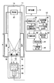
すなわち、本実施の形態に係るホログラムの欠陥検出方法を適用したホログラム欠陥検出装置は、被検体である薄板状のホログラム10の表面の欠陥を検出する装置であって、光照射部11と、画像データ処理部12と、表示装置14とを備えている。
【0060】
光照射部11は、被検体であるホログラム10を下部に配置させているとともに、撮像手段を固定する収納体16を備えている。また、収納体16の下部には、円筒状の光源18を備えている。
【0061】
光源18としては、蛍光管の如く点灯を繰り返す光源でも良いが、ハロゲンやキセノンなど直流点灯し、十分な強度を取れる光源がより好ましい。光源18は、発光部とそれを導光する透明もしくは半濁色の部材によって構成している。また、収納体16内部の上部側には、光源18に電力もしくは光束を供給する照光部20を備えている。
【0062】
この光源18の高さを十分にとることによって、ホログラム10の表面に対して実質的な全方向から検査光hを照射できるようにしている。
【0063】
このように、ホログラム10の表面側の全方向から検査光hが照射されると、このホログラム10に欠陥がない場合には、ホログラム10の表面の各場所で回折した回折光の中には、必ずホログラム10の表面に対して垂直方向に回折する回折光kが存在する。
【0064】
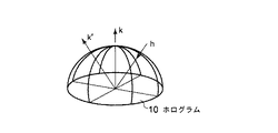
この理由は以下の通りである。すなわち、図2(a)に示すように、ホログラム10表面上のある微少領域において、該領域に対して垂直方向から絞った検査光hを照射すると、該領域を中心とした全天球(半球)21のどこかの方向に必ず回折光(1次)kが発生する。
【0065】
これは、図2(b)に示すように、逆に、回折光kが発生した方向から検査光hをホログラム10の該領域に照射すると、該領域に対して垂直方向に回折光kを生じるとも言える。
【0066】
なお、回折光は±1,±2,・・,±N次回折光の成分があるが、回折次数とは無関係であるため以下、1次回折光についてのみ言及する。
【0067】
これを利用すれば、全天球(半球)方向から検査光hを照射することにより、任意の回折角を持つホログラム10上の微少領域から、ホログラム10の表面に対して垂直方向に回折光kを生じさせることができる。ここで、垂直方向に撮像装置26を配置することにより、全ての微少領域から生じる回折光kを撮像するようにしている。
【0068】
この撮像装置26は、テレセントリックレンズ22およびカメラ24を備えている。
【0069】
テレセントリックレンズ22は、カメラ24とホログラム10との間に備えられ、垂直方向へ沿って直進する回折光kのみをカメラ24へと導く。テレセントリックレンズ22は、図3(a)に示すように、2枚のレンズ22(#a)とピンホールPとがセットになって構成されており、検査光hによって照射されたホログラム10の表面を、真上から見た像を撮像するのに適している。すなわち、図3(a)に示すように、テレセントリックレンズ22は、直進してくる光のみを使って結像するので、図3(a)中の記号aで示すように、斜めから入ってくる光は結像しない。このため、例えば円筒体25を真上から見た場合、図3(b)に示すように、胴部25(#a)と中空部25(#b)とからのみなる画像となる。
【0070】
一方、テレセントリックレンズではない一般の撮影レンズ27は、図4(a)に示すように、2枚のレンズ27がセットになって構成されており、図4(a)中の記号bに示すように、斜めから入ってくる光も結像する。このため、円筒体25を真上から見た場合であっても、図4(b)に示すように、胴部25(#a)と中空部25(#b)との間に内側面25(#c)が存在するように結像する。
【0071】
テレセントリックレンズ22は、片側テレセン、両側テレセンのどちらを使用しても可能であるが、撮像装置26における素子のサイズと撮像視野サイズの関係を満たす倍率であることが望ましい。
【0072】
カメラ24は、ライン型センサが望ましいが、エリア型センサを用いてもよい。そして、テレセントリックレンズ22によって導かれた回折光kを撮像し、光の強度からアナログの電気信号に変換し、更にデジタルの電気信号へ変換することによって画像データを生成する。そして、生成した画像データを画像データ処理部12へと出力する。なお、アナログの電気信号を画像データ処理部12へと出力し、画像データ処理部12においてアナログの電気信号をデジタル変換することによって画像データを生成するようにしても良い。
【0073】
また、後述するように、ホログラム10の品質は通常、可視光領域(波長λ=380〜780nm)で評価されることが多いため、可視光領域における検査について説明する。
【0074】
ホログラム10に対する検査光hの照射角度範囲に死角が無いことが理想であるが、撮像装置26が所定の物理的空間を占有するため、物理空間としての死角を完全になくすことは困難である。しかしながら、ホログラム10の諸特性を利用することにより、図1に示すように、収納体16の内部に撮像装置26を配置している場合であっても、ホログラム10の回折角に対する死角を実質的になくすことが可能である。その理由は以下の通りである。
【0075】
すなわち、一般にホログラム10の回折光特性を決定する因子として、回折格子ピッチd、ホログラム10の面方向の回折格子回折方向の向き、ホログラム面の法線方向とのなす入射角θi、出射角θo、検査光hの波長λがある。
【0076】
これらは、以下に示す(1)式の関係がある。
λ=d(sinθi+sinθo)・・・(1)
ここで、説明を簡単にするために、θi=0とする(検査光hをホログラム10の法線方向から照射する)と、以下に示す(2)式の通りとなる。
λ=d×sinθo・・・(2)
ここで、検査光hの波長λが可視光の場合、λ=380〜780nmであるから、θoの取りうる角度は、以下に示す(3)式および(3’)式の通りとなる。なお、本実施の形態では、光源18は左右対称であるため、90°以内の回折角のみを対象としても差し支えない。
arcsin(380/dmax)≦θo≦arcsin(780/dmin)
ただし、780/dmin<1の場合 ・・・(3)
arcsin(380/dmax)≦θo≦ 90°
ただし、780/dmin≧1の場合 ・・・(3’)
回折格子ピッチdは、ホログラム10の品種や製造条件等に依存するので一概には決められないが、500nm〜2500nm程度が多いとされている。この場合、出射角θo、すなわち検査光hの回折範囲は以下に示す(4)式の通りとなる。
10.95°≦θo≦90° ・・・・・(4)
すなわち、出射角θo<10.95°となる範囲は死角であり、この範囲では、ホログラム10に対する回折光kは存在しない。したがって、ホログラム10からの回折光kの出射範囲は、図5中にハッチングで示す領域となり、ハッチングで示されない領域が死角領域Jとなる。つまり、図5中に示す死角領域Jから検査光hをホログラム10に向けて照射しても、ホログラム10からの回折光kは存在しない。
【0077】
本実施の形態では、撮像装置26を、この死角領域Jに配置するようにしている。これによって、撮像装置26が、上述したような回折光kの撮像に影響を及ぼすことがないようにしている。
【0078】
また、検査光hの最小照射角は、出射角θoの最小値より小さければよく、円筒状の光源18の場合、このような条件を満たす高さHは、円筒内径をrとすると、上記(4)式と、以下に示す(5)式とにしたがって、
H≧r/tan(θo) ・・・(5)
下限方向(10.95°≦θo)のH≧230mmとなる(r=35mmの場合)。この高さHを取ることにより死角が発生しない。
【0079】
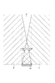
一方、上限方向(θo≦90°)では、ホログラム10に対して真横から検査光hを入射させることになるので、平坦なホログラム10の中心側の領域に対して検査光hを入射させることが困難なこと、あるいは光源18やホログラム10近辺の作業性が悪くなる等の装置構成上の理由から困難であることが多い。そこで、図6に示すように、ホログラム10を、光源18側から見て凸状に丸めた状態にして検査エリア30に供給するためのローラ28を備えている。
【0080】
このローラ28によってホログラム10を丸めた状態で検査エリア30に配置した状態で光源18から検査光hを照射することによって、通常は平坦なホログラム10であっても、表面の任意場所に対して、90°以上の角度からも検査光hを照射できるようにしている。
【0081】
以上のような構成によって、検査光hの照射角度範囲は下限方向検査光hmin(10.95°)から上限方向検査光hmax(90°)を含む範囲をカバーできるようになる。
【0082】
画像データ処理部12は、画像取込部32と、画像取込位置検出部34と、基準画像取込部36と、マスク画像生成部38と、欠陥抽出部40と、回折効率判定部42と、欠陥判定部44と、欠陥記録出力部46とを備えている。
【0083】
画像取込部32は、カメラ24から出力されたデジタルの電気信号である画像データを取得する。また、カメラ24からアナログの電気信号が出力された場合には、それをデジタルの電気信号である画像データへ変換する。この画像データは、図7にその一例を示すように、ホログラム10において回折格子がある部分は白く、回折格子がない部分は黒くなる。ホログラム10の回折格子に欠陥がある場合は、カメラ24には回折光kが入らないため、回折格子がない部分と同様に黒くなる。
【0084】
画像取込部32では、このようにして取得した画像データに対して、図8に示すフローチャートに従って動作し、エッジを鮮明化することにより、テレセントリックレンズ結像系の収差の補正を行い、補正した画像データを画像取込位置検出部34へと出力する。
【0085】
画像取込位置検出部34は、画像取込部32によって補正された画像データに対して、ホログラム10がローラ28によって取り込まれた際のタイミングのバラツキや、検査エリア30におけるホログラム10の走行時の位置ずれ補正を行う。この補正は、ホログラム10との位置関係が予め把握されている基準画像におけるホログラムマークの位置(フィレ座標、重心等)を測定することにより行う。この基準画像におけるマーク位置と、画像取込部32から出力された画像データのホログラムマークの位置との偏差が位置ずれ補正量である。画像取込位置検出部34は、このようにして位置ずれ補正した画像データを、要求に応じて基準画像取込部36、マスク画像生成部38、あるいは欠陥抽出部40へと出力するようにしている。
【0086】
ホログラム10がローラ28によって取り込まれた際のタイミングのバラツキや、検査エリア30におけるホログラム10の走行時の位置ずれに関する補足として、前述の死角の持つ意味について説明を加えておく。
【0087】
すなわち、死角とは、検査光hを照射しても回折光kが得られない範囲であるが、回折光kが得られないことは確かにデメリットの1つではある。しかし、自動検査の切り口から見ると、それは本質的な問題にはなりえない。より問題となることは、有効回折角である出射角θoの上限値、または下限値に近い回折光kを持つ回折格子の取り扱いである。
【0088】
元来、出射角θoは、ホログラム10の製造上のバラツキ、ホログラム10がローラ28によって取り込まれた際のタイミングのバラツキ、検査エリア30におけるホログラム10の走行時の位置ずれ、検査光hの色温度変動、ローラ28による供給中のホログラム10のバタツキ等様々な要因によって、ある範囲の変動幅を持っている。
【0089】
一方で、後述するように、欠陥検査の具体的方法としては、欠陥のない良品のホログラムの画像を基準画像とし、この基準画像の画像データと、カメラ24によって撮像された画像データとの相互相関、照合、あるいはパターンマッチングによって行う。このような方法は、任意のパターンに対処できることから、画像処理技術における主流の方法となっている。
【0090】
一般に、これらの方法では、被検体であるホログラム10の位置ずれが生じることを想定した上で、被写体であるホログラム10のパターンエッジ部をマスク(それ以外の方法もある)しているため、位置ずれによる擬似欠陥は発生しにくくなっている。
【0091】
また、欠陥を欠陥サイズで選別することにより、許容範囲の微少な欠陥による擬似欠陥も発生しにくくなっている。同様に、この方式でホログラム10の回折格子を検査した場合に、擬似欠陥として発生することが考えられるが、問題は、回折角度のバラツキにより生じる疑似欠陥に対するマスクをかけることが困難であることである。本実施の形態では、この問題を回避するため、ホログラム10の一次回折光kをすべて検出するように前述したような工夫をしている。
【0092】
基準画像取込部36は、画像取込位置検出部34によって補正された画像データの中から、自動的に、あるいは手動操作によって、良品と想定されるホログラム10の画像データを基準画像の画像データとして取得する。そして、この基準画像の画像データを、マスク画像生成部38および回折効率判定部42へと出力する。
【0093】
マスク画像生成部38は、基準画像取込部36から基準画像の画像データを取得する。基準画像の画像データの取得は、一度取り込んだ基準画像の画像データを保持しておき、保持した画像データを固定的に使用する場合、あるいは、基準画像取込部36から常時新たな基準画像の画像データを取得する場合の何れであっても良い。そして、基準画像の画像データに基づいて、図9に示すフローチャートにしたがって動作し、マスク画像データを生成する。そして、生成したマスク画像データを欠陥抽出部40へと出力する。
【0094】
このようなマスク画像の生成は、画像処理の分野において一般的に用いられている手法を用いて行う。このようなマスク画像の生成手法は、種々あるが、ここでは2つの例を挙げておく。
【0095】
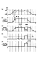
第1の例として、基準画像に対して、ミニマムフィルタを複数回施す方法がある。この方法について図10および図11を用いて説明する。図10(a)は、欠陥のないホログラム10について撮影された画像データの一例を示すものであって、図10(b)は、欠陥のあるホログラム10について撮影された画像データの一例を示すものである。また、図11(a)は、図10(a)に示す画像データにおけるA−A’線に沿って示した輝度分布である。横軸がA−A’線に沿った方向における位置、縦軸が輝度に相当する。
【0096】
ミニマムフィルタとは、近傍領域(カーネルともいう)において、その中で一番暗い値と中心画素(注目画素ともいう)の値とを置換する。図11(b)は、ミニマムフィルタの概念を説明するための図であって、図11(a)に示す輝度分布において、連続する3つの領域について着目し、その3つの領域の中で一番暗い値を中心画素に置換した例を示している。図11(a)と図11(b)とを比較して明らかなように、この置換処理により生成された図11(b)に示すようなミニマム画像では、画像パターンにおけるエッジ部のように明暗の変化が激しい部分は、暗輝度に広がりを持っていき、かつその部分も完全に非検査にはならないため、位置ずれ用のマスク(グレイマスク)として使用する。
【0097】
第2の例として、基準画像の画像データを2値化した後に微分系(ラプラシアン、ソーベル等)のフィルタを施す方法がある。この微分フィルタ処理により、画像パターンにおけるエッジ部を完全にマスクする。
【0098】
欠陥抽出部40は、画像取込位置検出部34によって位置ずれ補正された画像データを画像取込位置検出部34から、マスク画像生成部38によって生成されたマスク画像データをマスク画像生成部38からそれぞれ取得する。そして、取得した画像データとマスク画像データとに基づいて、図12に示すフローチャートにしたがって動作することにより、ホログラム10における欠陥候補部を抽出する。そして、その抽出結果を欠陥判定部44へと出力する。
【0099】
回折効率判定部42は、画像取込位置検出部34によって位置ずれ補正された画像データを画像取込位置検出部34から、基準画像の画像データを基準画像取込部36からそれぞれ取得する。そして、ホログラム10における回折格子の回折効率を判定し、判定結果を欠陥判定部44へと出力する。
【0100】
欠陥判定部44は、欠陥抽出部40によって抽出されたホログラム10における欠陥候補部とに基づいて、図13のフローチャートに示すように動作することによって、欠陥候補部が欠陥であるか否かを判定し、判定結果を欠陥記録出力部46へと出力する。
【0101】
欠陥記録出力部46は、欠陥判定部44から出力された判定結果に基づいて、欠陥部に対応する画像データや位置情報を表示装置14から表示させる。この場合、表示装置14からは、必要に応じて警報が吹鳴されるようにしても良い。
【0102】
本実施の形態に係るホログラムの欠陥検出方法を適用したホログラム欠陥検出装置は、上述したようにして、ホログラム10の回折格子の欠陥を検出する。なお、上述した検出方法は、既に製造されたホログラム10の画像に対して発生した欠陥の検出方法を例に説明しているが、本実施の形態に係るホログラムの欠陥検出方法を適用したホログラム欠陥検出装置は、既に製造されたホログラム10に対してのみならず、ホログラム10の製造時に発生する欠陥に対しても欠陥判定を可能としている。
【0103】
ホログラムの製造工程の一部には、フィルム上にホログラムを形成する工程がある。この工程では、ホログラムを形成するフィルムを走行させながら、図示しない版にフィルムを巻き付けた状態で圧力を加えることによってホログラムを形成している。この場合、版に異物等が付着してしまうと、その部分のホログラムが形成されず、連続して欠陥が形成されてしまう。
【0104】
このような場合には、1枚のホログラムの画像データに対する欠陥判定に加えて、複数のホログラムの画像データの同一箇所に規則的に発生した欠陥を連続性に判定することにより、版の異物付着により発生した欠陥を容易に検出できるようにしている。
【0105】
また、上述した例では、1つのホログラム10毎に欠陥検出を行う場合を例に説明しているが、図14に示すように、収納体16内の検査エリア30に複数のホログラム10(#1,#2,#3)を配列させた場合であっても、光源18および撮像装置26を移動可能な状態に配置し、これらを適宜移動させ、複数のホログラム10(#1,#2,#3)のうちの対象とするホログラム10に対して検査可能な状態を実現し、順番に検査を行うことによって、複数のホログラム10を対象とした欠陥検出を行うことも可能としている。
【0106】
あるいは、撮像装置26を複数設け、それぞれが、担当するホログラム10を検査することによって、複数のホログラム10を対象とした欠陥検出を行うことも可能としている。
【0107】
次に、以上のように構成した本実施の形態に係るホログラムの欠陥検出方法を適用したホログラム欠陥検出装置の作用について説明する。
【0108】
すなわち、本実施の形態に係るホログラムの欠陥検出方法を適用したホログラム欠陥検出装置を用いて、被検体であるホログラム10の表面における欠陥の有無を判定するためには、まず、検査エリア30にホログラム10を、その表面を上、すなわちカメラ24の側に向けて配置する。この場合、カメラ24が、ホログラム10の表面に対する法線方向から撮影できるようにホログラム10を検査エリア30に設置する。
【0109】
このようにして検査エリア30に被検体であるホログラム10が配置されると、次に、光源18によってホログラム10の表面側に向けて可視光である検査光hが照射される。検査光hがホログラム10の表面で回折し、ホログラム10の全域から法線方向への回折光kを得られるようにするためには、検査光hとして可視光を用いた場合、検査光hの照射角度範囲は下限方向検査光hmin(10.95°)から上限方向検査光hmax(90°)を含む範囲はもとより、その上更にホログラム10の製造上のバラツキ、ホログラム10がローラ28によって取り込まれた際のタイミングのバラツキ、検査エリア30におけるホログラム10の走行時の位置ずれ、検査光hの色温度変動、ローラ28による供給中のホログラム10のバタツキ等様々な要因を考慮した範囲をカバーできなければならない。
【0110】
これに対し、光源18は十分な高さHがとられているので、下限方向検査光hmin(10.95°)はもとより、上述したような変動要因をも考慮した領域がカバーされて照射される。また、ホログラム10は検査エリア30までローラ28によって搬送され、そのままローラ28によって丸めた状態で検査エリア30に配置されることによって、上限方向検査光hmax(90°)はもとより、上述したような変更要因をも考慮した領域がカバーされて照射される。
【0111】
これによって、ホログラム10は、実質的に表面側の全方向から検査光hが照射され、ホログラム10の全領域から、ホログラム10の表面に対して法線方向に向かって進む回折光kが発せられる。同時に、ホログラム10の表面からは、法線方向に沿って進む回折光k以外にも、様々な方向へと高次の回折光が発せられる。
【0112】
このように回折光は、様々な方向へと発せられるが、収納体16内部に配置された撮像装置26の先端側には、テレセントリックレンズ22が取り付けられているので、このテレセントリックレンズ22によって、法線方向に向かって進む回折光kのみが抽出され、カメラ24へと導かれる。
【0113】
なお、上述したように撮像装置26は、収納体16内部に配置されているが、光源18から発せられる検査光hの照射角度範囲に該当しない領域に配置されているので、回折光kが得られる角度からの検査光hのホログラム10への照射は阻害されない。
【0114】
そして、カメラ24によって、テレセントリックレンズ22から導かれた回折光kが撮像され、光の強度からアナログの電気信号へ、更にはアナログの電気信号からデジタルの電気信号への変換がなされることによって画像データが生成される。この画像データは、画像データ処理部12側へと出力される。なお、アナログの電気信号のまま画像データ処理部12へと出力され、画像データ処理部12におけるデジタル変換によって画像データが生成されるようにしても良い。
【0115】
このように、ホログラム10の表面に対して、実質的な表面側全方向から検査光hが照射された場合の作用について、図2(b)を用いて説明する。
【0116】
すなわち、ホログラム10の表面に対して、実質的な表面側全方向から検査光hを照射すると、ホログラム10における回折格子によって、ホログラム10の表面に対する法線方向に進む回折光kは必ず発生する。
【0117】
しかしながら、回折格子が潰れて平らになっている等により欠陥がある領域からは、例えば図15中に示すように、検査光hに対する直接反射光k’のみとなり、真上(法線方向)から検査光hが照射されない限り、法線方向に向かって進む回折光kは存在しなくなる。このように、法線方向への回折光kが存在しない状態で撮像された画像データには、図7に示すように欠陥場所が黒い点として表れる。
【0118】
カメラ24によって撮像されたこのような画像データは、画像データ処理部12側へ出力され、画像取込部32によって取得される。
【0119】
画像取込部32では、このようにして取得した画像データに対して、図8に示すフローチャートに示すような補正処理がなされ、補正された画像データが画像取込位置検出部34へと出力される。
【0120】
すなわち、画像取込部32では、画像データが取り込まれる(S1)と、この画像データに対してビニング処理が施され(S2)、コントラスト補正がかけられ(S3)、Kメディアンフィルタ等によってノイズ成分が除去され(S4)、しかる後にエッジのシャープ化処理がなされる(S4)。
【0121】
画像取込位置検出部34では、画像取込部32によって補正された画像データに対して、ホログラム10がローラ28によって取り込まれた際のタイミングのバラツキや、検査エリア30におけるホログラム10の走行時の位置ずれ補正が行われる。画像取込位置検出部34によって位置ずれ補正された画像データは、基準画像取込部36、マスク画像生成部38、あるいは欠陥抽出部40へと出力される。
【0122】
基準画像取込部36では、画像取込位置検出部34によって補正された画像データの中から、自動的に、あるいは手動操作によって、良品と想定されるホログラム10の画像データが基準画像の画像データとして取得される。そして、この基準画像の画像データが、マスク画像生成部38および回折効率判定部42へと出力される。
【0123】
マスク画像生成部38では、基準画像取込部36から出力された基準画像の画像データが取得される。なお、基準画像の画像データの取得は、一度取り込んだ基準画像の画像データを保持しておき、保持した画像データを固定的に使用する場合、あるいは、基準画像取込部36から常時新たな基準画像の画像データを取得する場合の何れであっても良い。そして、基準画像の画像データに基づいて、マスク画像データが生成され、このマスク画像データは欠陥抽出部40へと出力される。マスク画像データの種類についてはいくつかあるが、ここではミニマムフィルタを用いてマスク画像を生成する方法について図9に示すフローチャートを用いて説明する。
【0124】
すなわち、マスク画像生成部38では、基準画像の画像データを取得するタイミングになると(S11:Yes)基準画像取込部36から出力された基準画像の画像データが取得される(S12)。そして、取得された画像データに対するマスク画像データであるミニマム画像(MIN画像)データが生成される(S13)とともに、マーク位置が計測される(S14)。
【0125】
次に、上記のように作成されたマスク画像を用いた欠陥検査のフローを図12に示す。すなわち、所定のタイミングになると(S21:Yes)、画像取込部32によって画像データが取り込まれる(S22)。一方、図9のフローによって得られたマスク画像である基準画像に対する位置ずれ量を取得する(S23)。次に、その位置ずれ量に基づいて画像データの位置ずれ量を補正する(S24)。次に、検査画像とマスク画像とのFIX差分をとる(S25)。
【0126】
ここで、FIX差分について説明する。FIX差分とは、マスク画像Aと画像データBとのFIX差分をFIX(A−B)としたとき、
A>B場合 FIX(A−B)=A−B
A≦Bの場合 FIX(A−B)=0
によって求める。これを、図11(b)に示すマスク画像と、図11(c)に示す画像データとにあてはめたとき、FIX差分の結果は、図11(d)に示す通りとなる。
【0127】
更に、図11(d)に示すようなFIX差分に対して、予め定めたしきい値αより大きい値を「1」、それ以下の値を「0」とする2値化処理がなされる(S26)。この2値化処理によって「1」とされた部分が欠陥候補部として抽出される。
【0128】
回折効率判定部42には、位置ずれ補正された画像データが画像取込位置検出部34から、基準画像の画像データが基準画像取込部36からそれぞれ入力される。回折効率判定部42では、これらに基づいてホログラム10における回折格子の回折効率が判定され、判定結果が欠陥判定部44へと出力される。
【0129】
欠陥判定部44では、欠陥抽出部40によって抽出されたホログラム10における欠陥候補部に基づいて、図13のフローチャートに示すように動作することによって、欠陥候補部が欠陥であるか否かが判定される。そして、判定結果が欠陥記録出力部46へと出力される。この欠陥判定の方法について、図13に示すフローチャートを用いて説明する。
【0130】
すなわち、図16(a)に示される画像データには、実際の欠陥の他に、疑似欠陥も含まれている可能性がある。したがって、イロージョン/ダイレーションが一定回数繰り返されることにより、図16(b)に示すように、疑似欠陥と見なされる欠陥候補部が取り除かれる。あるいは、大きな欠陥候補部のひび割れ等が取り除かれる(S31)。
【0131】
次に、ステップS31で残った欠陥候補部に対して、図16(c)に示すように、ラベリングが施され(S32)、ラベルされた各欠陥候補部の面積が求められる(S33)。
【0132】
更に、ステップS33で面積が求められた欠陥候補部について、予め定めた判定しきい値との比較がなされ、許容値を超える欠陥候補部が欠陥と判定される(S34)。判定結果の一例を図17に示す。ここでは、判定しきい値である面積を「10」としており、面積が判定しきい値を超える欠陥候補部(ラベル2,5)が欠陥と判定され、面積が判定しきい値以下である欠陥候補部(ラベル1,3,4)については欠陥ではないと判定される。なお、この判定しきい値は、必ずしも固定値である必要はない。例えば、被検査体であるホログラムの近傍に、回折方向と回折格子ピッチが既知のホログラムパターンを付加することにより、この場所の回折光強度に応じた閾値を設定することも可能である。
【0133】
更に、連続して欠陥検出を行う場合(S35:Yes)には、その旨が表示装置14から表示され(S36)、ステップS21の処理に戻る。欠陥検出を終了する場合(S35:No)であって、欠陥記録出力部46に、欠陥判定部44から判定結果が出力された場合(S37:Yes)には、欠陥部に対応する画像データや位置情報が表示装置14から表示される。この場合、必要に応じて警報もまた吹鳴され(S38)、ステップS21の処理に戻る。欠陥がなかった場合(S37:No)には、ステップS21の処理に戻る。
【0134】
本実施の形態に係るホログラムの欠陥検出方法を適用したホログラム欠陥検出装置は、上述したようにして、ホログラム10の表面に対して、実質的な表面側全方向から検査光hを照射し、更に、この検査光hがホログラム10の表面で回折してなる回折光のうち、ホログラム10の表面に対する法線方向に進む回折光kのみによる画像データを得ることができる。
【0135】
そして、ホログラム10の表面に欠陥がある場合には、この画像データの中には、黒い点として撮像されるので、この黒い点を画像処理により把握することによって、ホログラム10の欠陥を高精度でかつ容易に検出することができる。
【0136】
また、任意の品質のホログラムに対して汎用的に利用できることから、ホログラムの欠陥検出効率の向上を図ることも可能となる。
【0137】
なお、上述した検出方法は、既に製造されたホログラム10の画像に対して発生した欠陥の検出方法を例に説明しているが、本実施の形態に係るホログラムの欠陥検出方法を適用したホログラム欠陥検出装置は、既に製造されたホログラム10に対してのみならず、1枚のホログラム10の画像データに対する欠陥判定に加えて、複数のホログラム10の画像データの同一箇所に規則的に発生した欠陥を連続性に判定することにより、版の異物付着により発生した欠陥をも容易に検出することができる。
【0138】
また、図14に示すように、検査エリア30に複数のホログラム10(#1〜#3)が同時に配置された場合であっても、撮像装置26を移動可能な状態に配置し適宜移動させることによって、あるいは、撮像装置26を複数配置することによって、これらホログラム10(#1〜#3)の何れをも収納体16から取り出すことなく連続的に欠陥検出を行うことも可能である。
【0139】
(第2の実施の形態)
本発明の第2の実施の形態を図18を用いて説明する。
【0140】
すなわち、本実施の形態に係るホログラムの欠陥検出方法を適用したホログラム欠陥検出装置は、第1の実施の形態に係るホログラムの欠陥検出方法を適用したホログラム欠陥検出装置の変形例であって、その構成を第1の実施の形態において説明した図1と同一とし、画像データ処理部12によってなされているデータ処理方法が異なるのみである。したがって、ここでは、異なる部分についてのみ述べる。
【0141】
すなわち、本実施の形態に係るホログラムの欠陥検出方法を適用したホログラム欠陥検出装置では、欠陥抽出部40において、画像取込位置検出部34によって位置ずれ補正された画像データと、マスク画像生成部38によって生成されたマスク画像データとを比較する。
【0142】
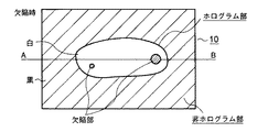
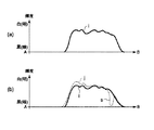
比較結果の一例を図18に示す。図18(a)は、マスク画像生成部38から出力された基準画像の画像データのうち、図10(a)に示すように、基準とするホログラム10について撮影された画像データにおける任意線AB線に沿って示した輝度分布iである。横軸がAB方向における位置、縦軸が輝度に相当する。一方、図18(b)は、図10(a)に示す基準とするホログラム10の輝度分布iに対して、図10(b)に示すように、欠陥があるホログラム10のAB線に沿って示した輝度分布jを合わせて表示した図である。
【0143】
図18(b)に示すように、輝度分布iと輝度分布jとは、AB線に沿った輝度分布が大部分類似しているものの、輝度分布jには、輝度分布iに対して有意に暗輝度側に突出しているピークsがある。ホログラム10の表面に欠陥があると、画像データには、欠陥がある場所が黒い点として撮像される。このため、ピークsに示すように輝度が暗輝度側に突出するようになる。
【0144】
欠陥抽出部40は、このように、基準画像の輝度分布iに対して、有意に暗輝度側に突出しているピークsがある場合、このピークsに対応する位置を欠陥候補部として抽出する。
【0145】
上述したような構成とすることによっても、第1の実施の形態と同様の作用効果を奏することができる。
【0146】
(第3の実施の形態)
本発明の第3の実施の形態を図19から図20を用いて説明する。
【0147】
すなわち、本実施の形態に係るホログラムの欠陥検出方法を適用したホログラム欠陥検出装置は、第1の実施の形態に係るホログラムの欠陥検出方法を適用したホログラム欠陥検出装置の変形例であって、その構成を第1の実施の形態において説明した図1と同一とし、検査対象であるホログラム10にホログラムマークmを付した点のみが異なる。したがって、ここでは、異なる部分についてのみ述べる。
【0148】
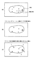
すなわち、本実施の形態に係るホログラムの欠陥検出方法を適用したホログラム欠陥検出装置では、図19に示すように、検査対象であるホログラム10にホログラムマークmを付している。
【0149】
このホログラムマークmは、回折方向および回折格子が予め把握されており、検査対象としているホログラムパターンnとの相対位置もまた予め把握された位置に配置されるようにしている。
【0150】
そして、本実施の形態に係るホログラムの欠陥検出方法を適用したホログラム欠陥検出装置は、このようなホログラムパターンnが付されたホログラム10に対しても、第1および第2の実施の形態で説明したものと同様にして、画像データを取得し、取得した画像データに基づいて欠陥有無の判定を行う。
【0151】
以上のように構成した本実施の形態に係るホログラムの欠陥検出方法を適用したホログラム欠陥検出装置によって、フィルム上に規則的に回折格子が製作されたホログラム10を図示しない巻取手段によって巻き取ることによって検査エリア30の所定位置に、検査対象とするホログラムパターンnが載置されるようにホログラム10を配置する場合、このホログラムマークmを検知することによって、ホログラムパターンnの位置を把握することが可能となる。
【0152】
あるいは、ホログラムマークmからの回折光の強度と、欠陥のないホログラムパターンnとの回折光の強度との比を予め把握しておくことによって、ホログラムパターンnの欠陥検出を行うことも可能となる。
【0153】
以上、本発明の好適な実施の形態について、添付図面を参照しながら説明したが、本発明はかかる構成に限定されない。特許請求の範囲に記載された技術的思想の範疇において、当業者であれば、各種の変更例及び修正例に想到し得るものであり、それら変更例及び修正例についても本発明の技術的範囲に属するものと了解される。
【0154】
例えば、上記実施の形態では、反射型のホログラム10について説明したが、本発明のホログラムの欠陥検出装置および欠陥検出方法では、以下のようにして、透過型のホログラムの欠陥検出を行うようにすることもできる。
【0155】
この場合、図20に示すように、撮像装置26を、検査エリア30に設置されたホログラム10の背面側に配置する。そして、光源18から検査光hを照射し、この検査光hがホログラム10を透過してなる回折光のうち、ホログラム10の表面に対して法線方向の回折光kのみをテレセントリックレンズ22が抽出してカメラ24へと導く。
【0156】
このような構成とすることによっても、透過型のホログラムに対しても同様に、欠陥の検出を行うことができる。
【0157】
【発明の効果】
以上説明したように、本発明のホログラムの欠陥検出方法を適用したホログラム欠陥検出装置によれば、ホログラムの表面に対して、実質的な表面側全方向から検査光を照射し、更に、この検査光がホログラムの表面で回折してなる回折光のうち、ホログラムの表面に対する法線方向に進む回折光のみによる画像データを得ることができる。
【0158】
そして、ホログラムの表面に欠陥がある場合には、この画像データの中には、黒い点として撮像されるので、この黒い点を画像処理により把握することによって、高精度でかつ容易に欠陥を検出することができる。
【0159】
また、任意の品質のホログラムに対して汎用的に利用できることから、ホログラムの欠陥検出効率の向上を図ることも可能となる。
【図面の簡単な説明】
【図1】第1の実施の形態に係るホログラムの欠陥検出方法を適用したホログラム欠陥検出装置の一例を示す機能構成図
【図2】ホログラムによる回折光の回折方向を説明するための図
【図3】テレセントリックレンズの原理を説明するための模式図
【図4】非テレセントリックレンズの原理を説明するための模式図
【図5】第1の実施の形態に係るホログラムの欠陥検出方法を適用したホログラム欠陥検出装置において撮像装置を配置する空間を示す図
【図6】検査エリアに配置されたホログラムを示す詳細図
【図7】欠陥のあるホログラムの画像データの一例を示す模式図
【図8】画像取込部によってなされる補正処理の流れを示すフローチャート
【図9】マスク画像生成部によってなされるマスク画像データの生成方法の流れを示すフローチャート
【図10】欠陥のないホログラムの画像データの一例、および欠陥のあるホログラムの画像データの一例を示す模式図
【図11】欠陥候補部を抽出するための画像処理の概念を示す図
【図12】欠陥抽出部によってなされる欠陥候補部の抽出方法の流れを示すフローチャート
【図13】欠陥判定部によってなされる欠陥判定方法の流れを示すフローチャート
【図14】収納体の検査エリアに複数のホログラムが配置された場合の一例を示す平面図
【図15】ホログラム表面の欠陥において回折する回折光の方向を説明するための図
【図16】欠陥を抽出するための処理を説明するための図
【図17】欠陥候補部の面積と欠陥判定結果の一例を示す図
【図18】ホログラム表面の任意方向に沿った輝度分布の一例を示す模式図
【図19】ホログラムマークが付されたホログラムの一例を示す模式図
【図20】ホログラムを透過した回折光を用いてホログラムの欠陥を検出するための装置の一例を示す機能構成図
【符号の説明】
h…検査光、k…回折光、k’…直接反射光、d…回折格子ピッチ、φ…回折格子回転角、θi…入射角、θo…出射角、λ…波長、J…死角領域、hmin…下限方向検査光、hmax…上限方向検査光、i…輝度分布、j…輝度分布、s…ピーク、m…ホログラムマーク、n…ホログラムパターン、P…ピンホール、10…ホログラム、11…光照射部、12…画像データ処理部、14…表示装置、16…収納体、18…光源、20…照光部、21…全天球、22…テレセントリックレンズ、24…カメラ、25…円筒体、25(#a)…胴部、25(#b)…中空部、25(#c)…内側面、26…撮像装置、27…撮影レンズ、28…ローラ、30…検査エリア、32…画像取込部、34…画像取込位置検出部、36…基準画像取込部、38…マスク画像生成部、40…欠陥抽出部、42…回折効率判定部、44…欠陥判定部、46…欠陥記録出力部[0001]
TECHNICAL FIELD OF THE INVENTION
The present invention relates to a defect detection apparatus and a defect detection method for detecting a defect of a hologram, particularly a defect or a defect of a diffraction grating itself.
[0002]
[Prior art]
Normally, a transfer type hologram is obtained by transferring a diffraction grating pattern to a resin surface by pressing a stamper having a relief-shaped diffraction grating recorded on a plane, for example, against a resin surface, and then depositing a metal on the surface to form a reflection layer. It is manufactured by being. Of course, various materials other than resin may be used.
[0003]
The designs of the holograms manufactured in this way are various, and the diffraction directions are various and take any direction. As a result, the hologram can reproduce images of various patterns depending on the angle of incidence of light. Therefore, the hologram can be applied to an IC card or a credit card to prevent forgery or to control security. . As described above, since the hologram is applied to forgery prevention, security management, and the like, it is required to reliably manufacture the hologram.
[0004]
However, since the hologram as described above is precisely formed by micron-order and very complicated diffraction grating patterns, its production is not easy, and it is necessary to pay sufficient attention to the production stage. is there.
[0005]
For example, when a hologram is manufactured in a state where foreign matter such as dust adheres to the stamper and the foreign matter is still attached, every time the stamper is pressed, the unevenness of the diffraction grating is crushed, and a correct diffraction grating pattern is obtained on the surface. Can not be. Therefore, even after manufacturing, it is necessary to strictly inspect for defects.
[0006]
[Problems to be solved by the invention]
However, it is not easy to detect a hologram defect as described below.
[0007]
That is, since the hologram usually sees diffracted light, the appearance of the image changes depending on the viewpoint. For this reason, it is not possible to view all images at once under direct reflected light or under illumination conditions using one or more light sources. Further, the visible image changes due to a slight difference in light irradiation conditions. Therefore, the image to be inspected is not stable, and the inspection result cannot maintain reliability.
[0008]
Therefore, in practice, the most realistic and easy method is to perform an inspection using an inspection apparatus including a light irradiation system and an imaging system whose angle is fixed according to the type of hologram.
[0009]
However, each time the type of the hologram to be inspected is changed, the inspection after adjusting the light irradiation system and the imaging system is not an easy operation itself, but requires labor and time. Further, depending on the diffraction angle taken by the hologram, there may be a case where diffracted light cannot be obtained due to the structure of the inspection device and only a partial inspection can be performed.
[0010]
Under such circumstances, automatically inspecting a hologram of an arbitrary type is not realistic at all, and the quality of the hologram must rely on a visual check for a part or most of the hologram.
[0011]
Therefore, even if a correct diffraction grating is not formed on the surface and a defective hologram is produced, it is difficult to detect the defect, and there is a possibility that a large number of defective holograms will be produced continuously. There is a problem.
[0012]
The present invention has been made in view of such circumstances, and has a hologram defect detection method that can be generally used for detecting a defect of a hologram of any type and that can accurately detect the defect. It is an object to provide an apparatus and a defect detection method.
[0013]
[Means for Solving the Problems]
In order to achieve the above object, the present invention takes the following measures.
[0014]
That is, the invention of
[0015]
Therefore, in the hologram defect detection apparatus according to the first aspect of the present invention, by taking the above measures, if the hologram surface has a defect, the inspection light does not diffract in the normal direction. In the image data viewed from the line direction, a defective portion is imaged as a black dot.
[0016]
Therefore, when this black dot is observed, it is possible to detect a defect on the surface of the hologram with high accuracy by determining that the surface of the hologram has a defect.
[0017]
According to a second aspect of the present invention, in the hologram defect detection apparatus according to the first aspect of the present invention, the diffracted light extracting means extracts, as the diffracted light, the light traveling along the normal direction from the reflected light.
[0018]
Therefore, in the hologram defect detection apparatus according to the second aspect of the present invention, by taking the above-described means, the diffracted light extracting means converts only the light that travels along the normal direction out of the reflected light as the diffracted light. Can be extracted. Thereby, the hologram defect detection accuracy can be improved.
[0019]
The invention according to
[0020]
Therefore, in the hologram defect detection apparatus according to the third aspect of the present invention, by taking the above-described means, the image data of the diffracted light that has been captured is compared with the image data of the normal hologram that has been captured in advance. As a result, a defect can be detected with high accuracy.
[0021]
According to a fourth aspect of the present invention, in the hologram defect detection apparatus according to the third aspect of the present invention, the diffracted light extracting means extracts, as transmitted light, light traveling along the normal direction as diffracted light.
[0022]
Therefore, in the hologram defect detecting device according to the fourth aspect of the present invention, by taking the above-described means, the diffracted light extracting means converts only the light traveling along the normal direction of the transmitted light into the diffracted light. Can be extracted. Thereby, the hologram defect detection accuracy can be improved.
[0023]
According to a fifth aspect of the present invention, in the hologram defect detecting apparatus according to the second or fourth aspect, a telecentric lens is provided between the imaging unit and the hologram, and guides light traveling in a normal direction to the imaging unit. Is used as a diffracted light extraction means.
[0024]
The telecentric lens captures only light traveling along the normal direction among the diffracted light from the hologram irradiated by the inspection light. Therefore, in the hologram defect detecting device according to the fifth aspect of the present invention, by taking the above-described means, if there is a defect on the surface of the hologram, it is determined as a black point in the image data viewed from the normal direction. Images can be taken. As a result, it is possible to accurately detect a defect on the surface of the hologram.
[0025]
According to a sixth aspect of the present invention, in the hologram defect detection apparatus according to any one of the first to fifth aspects, of the diffracted light diffracted by the hologram, the diffracted light travels along the normal direction and the imaging means. The diffracted light extracting means is arranged on the normal direction side of the irradiation angle range of the inspection light with respect to the hologram such that the diffracted light in the wavelength region that can be imaged can be obtained.
[0026]
Therefore, in the hologram defect detection device according to the sixth aspect of the present invention, by taking the above-described means, the inspection light is not interfered by the diffracted light extraction means, and substantially all of the surface of the hologram is exposed to the hologram. The inspection light can be emitted from the direction. Thereby, the defect inspection can be performed without blind spots over the entire surface of the hologram. Note that the irradiation angle range of the inspection light with respect to the hologram such that diffracted light in a wavelength region that can be imaged by the imaging means is indicated by the regions K and L in FIG.
[0027]
According to a seventh aspect of the present invention, in the hologram defect detection apparatus according to any one of the first to sixth aspects, of the diffracted light diffracted by the hologram, the light travels along the normal direction, and the imaging means. The inspection light source is arranged so that the inspection light can be irradiated from the surface side including the surface of the hologram, rather than the irradiation angle range of the inspection light to the hologram such that diffracted light in a wavelength region that can be imaged can be obtained. And a roller for rounding the hologram so as to be convex when viewed from the inspection light source. Then, by irradiating the inspection light from the inspection light source in a state where the hologram is rolled by the roller, the inspection light is irradiated at an arbitrary irradiation angle within an irradiation angle range to an arbitrary position on the surface of the hologram. I have.
[0028]
Therefore, in the hologram defect detecting device according to the seventh aspect of the present invention, by taking the above-described measures, the entire surface of the hologram can be irradiated with the inspection light even from a right angle. it can. Thereby, the defect inspection can be performed without blind spots over the entire surface of the hologram.
[0029]
According to an eighth aspect of the present invention, in the hologram defect detecting device according to any one of the first to seventh aspects, a hologram mark whose diffraction direction and diffraction pitch are grasped in advance is arranged near the hologram. The light source for inspection light irradiates the region including the surface of the hologram and the surface of the hologram mark with the inspection light, and the diffracted light extracting means inspects the inspection light from the reflected light that is reflected by the region. The light is diffracted by the hologram and the hologram mark to extract a diffracted light, and the imaging unit acquires image data by imaging the extracted diffracted light. Further, the determination means compares the light intensity of the portion corresponding to the hologram and the portion corresponding to the hologram mark in the obtained image data, and determines whether or not the hologram has a defect based on the comparison result. I am trying to do it.
[0030]
Therefore, in the hologram defect detection device according to the eighth aspect of the present invention, by taking the above-described means, the image data of the hologram to be inspected is compared with the hologram mark image data as a reference, whereby the inspection is performed. Defect inspection of the target hologram can be performed.
[0031]
According to a ninth aspect of the present invention, in the hologram defect detection apparatus according to any one of the first to seventh aspects, a hologram mark whose relative position, shape, diffraction direction, and diffraction pitch with respect to the hologram are grasped in advance is arranged. are doing. Then, the inspection light source irradiates the inspection light to the surface of the hologram mark, and the diffracted light extracting means diffracts the inspection light by the hologram mark from the reflected light formed by the inspection light being reflected by the hologram mark. Extract diffracted light. Further, the imaging unit acquires image data by imaging the extracted diffracted light, and the determination unit grasps the position of the hologram based on the acquired image data.
[0032]
Therefore, in the hologram defect detecting apparatus according to the ninth aspect of the present invention, by taking the above-described means, for example, even for a hologram continuously manufactured on a film, the position of the hologram mark is referred to. By performing the inspection, it is possible to inspect the hologram for defects while arranging the hologram image obtained by the imaging means at a correct position.
[0033]
According to a tenth aspect of the present invention, in the hologram defect detection apparatus according to any one of the first to ninth aspects, the determining means includes: a reference image luminance distribution obtained from previously captured reference image data; Is compared with the inspection image luminance distribution obtained from the image data acquired by the above, and it is determined that there is a defect in the inspection image luminance distribution at a position corresponding to a peak protruding toward the dark luminance side with respect to the reference image luminance distribution. Like that.
[0034]
If there is a defect in the hologram, there is no diffracted light in the direction normal to the hologram surface.Therefore, when diffracted light traveling along the normal direction is photographed, the defect location is photographed as a black dot in the image data. You. That is, in the luminance distribution based on the image data, the black point is detected as a peak protruding toward the dark luminance side with respect to the luminance distribution based on the image data of the hologram having no defect. Therefore, the hologram defect detection device according to the tenth aspect of the present invention can determine that there is a defect at the corresponding location by detecting the peak on the dark luminance side.
[0035]
The invention according to
[0036]
Therefore, in the hologram defect detection method according to the eleventh aspect of the present invention, by taking the above measures, if the hologram surface has a defect, the inspection light does not diffract in the normal direction. In the image data viewed from the line direction, a location having a defect is imaged as a black dot.
[0037]
Therefore, when this black dot is observed, it is possible to detect a defect on the surface of the hologram with high accuracy by determining that the surface of the hologram has a defect.
[0038]
According to a twelfth aspect of the present invention, in the hologram defect detection method according to the eleventh aspect, the diffracted light extracting means diffracts the light traveling along the normal direction among the reflected light obtained by reflecting the inspection light by the hologram. They are extracted as light.
[0039]
Therefore, in the hologram defect detection method according to the twelfth aspect of the present invention, by taking the above-described means, the diffracted light extracting means uses only the light traveling along the normal direction among the reflected lights as the diffracted light. Can be extracted. Thereby, the hologram defect detection accuracy can be improved.
[0040]
According to a thirteenth aspect of the present invention, there is provided a method for detecting a defect of a hologram, wherein the inspection light is irradiated from substantially all directions on the surface side except the normal direction to the surface of the hologram, and the inspection light is transmitted through the hologram. From the transmitted light, diffracted light obtained by diffracting the inspection light by the hologram is extracted by the diffracted light extracting means. Then, image data is obtained by imaging the extracted diffracted light by the imaging means, and it is determined whether or not the hologram has a defect based on the obtained image data and reference image data previously imaged. I am trying to do it.
[0041]
Therefore, in the hologram defect detection method according to the thirteenth aspect of the present invention, by taking the above means, the image data of the diffracted light that has been taken is compared with the image data of the normal hologram that has been taken in advance. As a result, a defect can be detected with high accuracy.
[0042]
According to a fourteenth aspect of the present invention, in the hologram defect detection method according to the thirteenth aspect, the diffracted light extracting means diffracts the light traveling along the normal direction, out of the transmitted light transmitted by the inspection light through the hologram. They are extracted as light.
[0043]
Therefore, in the hologram defect detection method according to the fourteenth aspect of the present invention, by taking the above-described means, the diffracted light extracting means uses only the light that travels along the normal direction among the transmitted light as the diffracted light. Can be extracted. Thereby, the hologram defect detection accuracy can be improved.
[0044]
According to a fifteenth aspect of the present invention, in the hologram defect detection method according to the twelfth or fourteenth aspect, a telecentric lens disposed between the imaging means and the hologram is used as the diffracted light extracting means.
[0045]
The telecentric lens captures only light traveling along the normal direction among the diffracted light from the hologram irradiated by the inspection light. Therefore, in the hologram defect detection method according to the fifteenth aspect of the present invention, by taking the above means, if there is a defect on the surface of the hologram, it is determined as a black point in the image data viewed from the normal direction. Images can be taken. As a result, it is possible to accurately detect a defect on the surface of the hologram.
[0046]
According to a sixteenth aspect of the present invention, in the hologram defect detection method according to any one of the eleventh to fifteenth aspects, of the diffracted light diffracted by the hologram, the diffracted light travels along the normal direction, and the imaging means The diffracted light extracting means is arranged on the normal direction side of the irradiation angle range of the inspection light with respect to the hologram such that the diffracted light in the wavelength region that can be imaged can be obtained.
[0047]
Therefore, in the hologram defect detection method according to the sixteenth aspect of the present invention, by taking the above-described means, the inspection light is not interfered by the diffracted light extraction means, and substantially all of the surface of the hologram is exposed to the hologram. The inspection light can be emitted from the direction. Thereby, the defect inspection can be performed without blind spots over the entire surface of the hologram.
[0048]
According to a seventeenth aspect of the present invention, in the hologram defect detection method according to any one of the eleventh to sixteenth aspects, of the diffracted light diffracted by the hologram, the diffracted light travels along the normal direction and the imaging means. Irradiation of inspection light from the side including the surface of the hologram, and irradiation of the hologram with the inspection light, rather than the irradiation angle range of the inspection light with respect to the hologram such that diffracted light in a wavelength region that can be imaged can be obtained. By irradiating the inspection light in a state where the inspection light is rounded so as to be convex when viewed from above, the inspection light is irradiated at an arbitrary irradiation angle within an irradiation angle range to an arbitrary position on the surface of the hologram.
[0049]
Therefore, in the hologram defect detection method according to the seventeenth aspect of the present invention, by taking the above measures, it is possible to irradiate the entire region of the hologram surface with the inspection light even from a right angle. it can. Thereby, the defect inspection can be performed without blind spots over the entire surface of the hologram.
[0050]
According to an eighteenth aspect of the present invention, in the hologram defect detection method according to any one of the eleventh to seventeenth aspects, a hologram mark whose diffraction direction and diffraction pitch are previously grasped is arranged near the hologram. A region including the surface and the surface of the hologram mark is irradiated with inspection light, and the inspection light is diffracted by the hologram and the hologram mark. Extract by the extraction means. Then, image data is obtained by imaging the extracted diffracted light by the imaging means, and the light intensity of the portion corresponding to the hologram and the light intensity of the portion corresponding to the hologram mark in the obtained image data is compared. It is determined whether or not the hologram has a defect based on the comparison result.
[0051]
Therefore, in the hologram defect detection method according to the eighteenth aspect of the present invention, by taking the above means, the inspection is performed by comparing the image data of the hologram to be inspected with reference to the image data of the hologram mark. Defect inspection of the target hologram can be performed.
[0052]
According to a nineteenth aspect of the present invention, in the hologram defect detection method according to any one of the eleventh to seventeenth aspects, a hologram mark whose relative position, shape, diffraction direction, and diffraction pitch with respect to the hologram are grasped in advance is arranged. Then, the inspection light is irradiated onto the surface of the hologram mark, and the diffracted light obtained by diffracting the inspection light by the hologram mark is extracted by the diffracted light extracting means from the reflected light obtained by reflecting the inspection light by the hologram mark. Then, image data is obtained by imaging the extracted diffracted light by the imaging means, and the position of the hologram is grasped based on the obtained image data.
[0053]
Therefore, in the hologram defect detection method according to the nineteenth aspect of the present invention, by taking the above-described means, for example, even for a hologram continuously manufactured on a film, the position of the hologram mark is referred to. By performing the inspection, it is possible to inspect the hologram for defects while arranging the hologram image obtained by the imaging means at a correct position.
[0054]
According to a twentieth aspect of the present invention, in the hologram defect detection method according to any one of the eleventh to nineteenth aspects, the reference image luminance distribution obtained from the previously captured reference image data and the hologram defect distribution obtained by the imaging means are provided. By comparing the inspection image luminance distribution obtained from the image data with the inspection image luminance distribution, it is determined that there is a defect at a position corresponding to a peak protruding toward the dark luminance side with respect to the reference image luminance distribution. .
[0055]
If there is a defect in the hologram, there is no diffracted light in the direction normal to the hologram surface.Therefore, when diffracted light traveling along the normal direction is photographed, the defect location is photographed as a black dot in the image data. You. That is, in the luminance distribution based on the image data, the black point is detected as a peak protruding toward the dark luminance side with respect to the luminance distribution based on the image data of the hologram having no defect. Accordingly, in the hologram defect detection method according to the twentieth aspect, by detecting the peak on the dark luminance side, it can be determined that there is a defect at the corresponding location.
[0056]
BEST MODE FOR CARRYING OUT THE INVENTION
Hereinafter, embodiments of the present invention will be described with reference to the drawings.
[0057]
(First Embodiment)
A first embodiment of the present invention will be described with reference to FIGS.
[0058]
FIG. 1 is a functional configuration diagram illustrating an example of a hologram defect detection apparatus to which the hologram defect detection method according to the first embodiment is applied.
[0059]
That is, the hologram defect detection device to which the hologram defect detection method according to the present embodiment is applied is a device that detects a defect on the surface of the
[0060]
The
[0061]
As the
[0062]
By making the height of the
[0063]
As described above, when the inspection light h is irradiated from all directions on the surface side of the
[0064]
The reason is as follows. In other words, as shown in FIG. 2A, when a certain small area on the surface of the
[0065]
Conversely, as shown in FIG. 2B, when the inspection light h is applied to the area of the
[0066]
Note that the diffracted light has components of ± 1, ± 2,..., ± Nth-order diffracted light, but since it has nothing to do with the diffraction order, only the first-order diffracted light will be described below.
[0067]
By utilizing this, the inspection light h is irradiated from the whole celestial sphere (hemisphere) direction, so that the diffracted light k from the minute area on the
[0068]
This
[0069]
The
[0070]
On the other hand, a general photographing lens 27 that is not a telecentric lens is configured by a set of two lenses 27 as shown in FIG. 4A, and as shown by a symbol b in FIG. In addition, the light that enters obliquely also forms an image. Therefore, even when the
[0071]
The
[0072]
The
[0073]
In addition, as will be described later, the quality of the
[0074]
Ideally, there is no blind spot in the irradiation angle range of the inspection light h to the
[0075]
That is, generally, factors that determine the diffracted light characteristics of the
[0076]
These have the relationship of the following equation (1).
λ = d (sin θi + sin θo) (1)
Here, for the sake of simplicity, when θi = 0 (the inspection light h is irradiated from the normal direction of the hologram 10), the following equation (2) is obtained.
λ = d × sin θo (2)
Here, when the wavelength λ of the inspection light h is visible light, λ is 380 to 780 nm. Therefore, the possible angles of θo are as shown in the following equations (3) and (3 ′). In the present embodiment, since the
arcsin (380 / dmax) ≦ θo ≦ arcsin (780 / dmin)
However, when 780 / dmin <1 (3)
arcsin (380 / dmax) ≦ θo ≦ 90 °
However, when 780 / dmin ≧ 1 (3 ′)
The diffraction grating pitch d cannot be unconditionally determined because it depends on the type of the
10.95 ° ≦ θo ≦ 90 ° (4)
That is, the range where the emission angle θo <10.95 ° is the blind spot, and in this range, the diffracted light k with respect to the
[0077]
In the present embodiment, the
[0078]
The minimum irradiation angle of the inspection light h may be smaller than the minimum value of the emission angle θo. In the case of the cylindrical
H ≧ r / tan (θo) (5)
H ≧ 230 mm in the lower limit direction (10.95 ° ≦ θo) (when r = 35 mm). By taking this height H, blind spots do not occur.
[0079]
On the other hand, in the upper limit direction (θo ≦ 90 °), the inspection light h is incident on the
[0080]
By irradiating the inspection light h from the
[0081]
With the above-described configuration, the irradiation angle range of the inspection light h is set to the lower limit direction inspection light h. min (10.95 °) to upper limit direction inspection light h max (90 °).
[0082]
The image
[0083]
The
[0084]
The
[0085]
The image capturing
[0086]
The meaning of the above-described blind spot will be additionally described as supplementary information on the timing variation when the
[0087]
That is, the blind spot is a range in which the diffracted light k cannot be obtained even when the inspection light h is irradiated, but the fact that the diffracted light k is not obtained is certainly one of the disadvantages. However, from the standpoint of automatic inspection, it cannot be an essential problem. What is more problematic is how to handle a diffraction grating having a diffracted light k that is close to the upper limit or lower limit of the output angle θo, which is the effective diffraction angle.
[0088]
Originally, the emission angle θo is a variation in the manufacturing of the
[0089]
On the other hand, as described later, as a specific method of the defect inspection, a non-defective non-defective hologram image is used as a reference image, and a cross-correlation between the image data of the reference image and the image data captured by the
[0090]
In general, in these methods, the pattern edge of the
[0091]
In addition, by selecting defects by defect size, pseudo defects due to minute defects within an allowable range are less likely to occur. Similarly, when the diffraction grating of the
[0092]
The reference
[0093]
The mask
[0094]
Generation of such a mask image is performed using a method generally used in the field of image processing. Although there are various methods for generating such a mask image, two examples will be given here.
[0095]
As a first example, there is a method of applying a minimum filter to a reference image a plurality of times. This method will be described with reference to FIGS. FIG. 10A shows an example of image data taken of a
[0096]
The minimum filter replaces the darkest value in the neighboring area (also called the kernel) with the value of the center pixel (also called the pixel of interest). FIG. 11B is a diagram for explaining the concept of the minimum filter. In the luminance distribution shown in FIG. 11A, attention is paid to three continuous areas, and the most significant among the three areas is shown. An example in which a dark value is replaced with a center pixel is shown. As is clear from a comparison between FIG. 11A and FIG. 11B, in the minimum image as shown in FIG. 11B generated by this replacement processing, the brightness is dark and light like an edge in the image pattern. The portion where the change is sharp is spread in the dark luminance, and the portion is not completely removed from the inspection. Therefore, the portion is used as a mask for displacement (gray mask).
[0097]
As a second example, there is a method of binarizing image data of a reference image and then applying a filter of a differential system (Laplacian, Sobel, etc.). The edge portion in the image pattern is completely masked by the differential filter processing.
[0098]
The
[0099]
The diffraction
[0100]
The
[0101]
The defect
[0102]
The hologram defect detection device to which the hologram defect detection method according to the present embodiment is applied detects a defect of the diffraction grating of the
[0103]
Part of the hologram manufacturing process includes a process of forming a hologram on a film. In this step, a hologram is formed by applying pressure while the film is wound around a plate (not shown) while running the film for forming the hologram. In this case, if a foreign substance or the like adheres to the plate, a hologram at that portion is not formed, and defects are continuously formed.
[0104]
In such a case, in addition to the defect determination for the image data of one hologram, the defect regularly occurring at the same position in the image data of a plurality of holograms is determined to be continuous, so that the foreign matter adhesion of the plate can be determined. This makes it possible to easily detect defects caused by the above.
[0105]
In the above-described example, the case where the defect detection is performed for each
[0106]
Alternatively, a plurality of
[0107]
Next, the operation of the hologram defect detection apparatus to which the hologram defect detection method according to the present embodiment configured as described above is applied will be described.
[0108]
That is, in order to use the hologram defect detection apparatus to which the hologram defect detection method according to the present embodiment is applied to determine whether or not there is a defect on the surface of the
[0109]
When the
[0110]
On the other hand, since the
[0111]
As a result, the
[0112]
As described above, the diffracted light is emitted in various directions. However, since the
[0113]
As described above, the
[0114]
Then, the
[0115]
The operation when the inspection light h is applied to the surface of the
[0116]
That is, when the surface of the
[0117]
However, as shown in FIG. 15, for example, as shown in FIG. 15, only the directly reflected light k ′ with respect to the inspection light h is obtained from the region where the diffraction grating is crushed and flattened. Unless the inspection light h is irradiated, there is no diffracted light k traveling in the normal direction. As described above, in the image data captured in a state where the diffracted light k does not exist in the normal direction, the defect location appears as a black point as shown in FIG.
[0118]
Such image data captured by the
[0119]
The
[0120]
That is, in the
[0121]
The image capturing
[0122]
In the reference
[0123]
In the mask
[0124]
That is, when it is time to acquire the image data of the reference image (S11: Yes), the mask
[0125]
Next, FIG. 12 shows a flow of a defect inspection using the mask image created as described above. That is, at a predetermined timing (S21: Yes), the image data is captured by the image capturing unit 32 (S22). On the other hand, the amount of displacement with respect to the reference image which is the mask image obtained by the flow of FIG. 9 is obtained (S23). Next, the displacement amount of the image data is corrected based on the displacement amount (S24). Next, a FIX difference between the inspection image and the mask image is obtained (S25).
[0126]
Here, the FIX difference will be described. When the FIX difference between the mask image A and the image data B is FIX (AB),
FIX (AB) = AB when A> B
When A ≦ B FIX (AB) = 0
Ask by. When this is applied to the mask image shown in FIG. 11B and the image data shown in FIG. 11C, the result of the FIX difference is as shown in FIG. 11D.
[0127]
Further, the FIX difference as shown in FIG. 11D is subjected to a binarization process in which a value larger than a predetermined threshold value α is “1” and a value smaller than the predetermined threshold α is “0” ( S26). The portion set to “1” by the binarization process is extracted as a defect candidate portion.
[0128]
The diffraction
[0129]
The
[0130]
That is, the image data shown in FIG. 16A may include a pseudo defect in addition to an actual defect. Therefore, by repeating the erosion / dilation a fixed number of times, as shown in FIG. 16B, a defect candidate portion regarded as a pseudo defect is removed. Alternatively, cracks and the like in the large defect candidate portion are removed (S31).
[0131]
Next, as shown in FIG. 16C, labeling is performed on the defect candidate portions left in step S31 (S32), and the area of each labeled defect candidate portion is obtained (S33).
[0132]
Further, the defect candidate part whose area is obtained in step S33 is compared with a predetermined determination threshold value, and a defect candidate part exceeding an allowable value is determined as a defect (S34). FIG. 17 shows an example of the determination result. Here, the area that is the determination threshold is set to “10”, and the defect candidate portions (
[0133]
Further, when the defect detection is performed continuously (S35: Yes), the fact is displayed on the display device 14 (S36), and the process returns to the step S21. If the defect detection is to be ended (S35: No), and if the determination result is output from the
[0134]
The hologram defect detection device to which the hologram defect detection method according to the present embodiment is applied irradiates the surface of the
[0135]
If there is a defect on the surface of the
[0136]
In addition, since holograms of any quality can be used for general purposes, it is possible to improve the efficiency of hologram defect detection.
[0137]
Although the above-described detection method has been described by taking as an example a method of detecting a defect that has occurred in an image of a
[0138]
Further, as shown in FIG. 14, even when a plurality of holograms 10 (# 1 to # 3) are simultaneously arranged in the
[0139]
(Second embodiment)
A second embodiment of the present invention will be described with reference to FIG.
[0140]
That is, the hologram defect detection device to which the hologram defect detection method according to the present embodiment is applied is a modified example of the hologram defect detection device to which the hologram defect detection method according to the first embodiment is applied. The configuration is the same as that of FIG. 1 described in the first embodiment, and only the data processing method performed by the image
[0141]
That is, in the hologram defect detection apparatus to which the hologram defect detection method according to the present embodiment is applied, in the
[0142]
FIG. 18 shows an example of the comparison result. FIG. 18A shows an arbitrary line AB in the image data of the
[0143]
As shown in FIG. 18B, although the luminance distribution i and the luminance distribution j are almost similar to each other along the AB line, the luminance distribution j is significantly different from the luminance distribution i. There is a peak s protruding toward the dark luminance side. If there is a defect on the surface of the
[0144]
When there is a peak s that significantly protrudes toward the dark luminance side with respect to the luminance distribution i of the reference image, the
[0145]
With the above-described configuration, the same operation and effect as the first embodiment can be obtained.
[0146]
(Third embodiment)
A third embodiment of the present invention will be described with reference to FIGS.
[0147]
That is, the hologram defect detection device to which the hologram defect detection method according to the present embodiment is applied is a modified example of the hologram defect detection device to which the hologram defect detection method according to the first embodiment is applied. The configuration is the same as that of FIG. 1 described in the first embodiment, except that the
[0148]
That is, in the hologram defect detection apparatus to which the hologram defect detection method according to the present embodiment is applied, as shown in FIG. 19, the
[0149]
In the hologram mark m, the diffraction direction and the diffraction grating are grasped in advance, and the relative position with respect to the hologram pattern n to be inspected is also arranged at a position grasped in advance.
[0150]
The hologram defect detection apparatus to which the hologram defect detection method according to the present embodiment is applied will be described in the first and second embodiments also for the
[0151]
By using the hologram defect detection apparatus to which the hologram defect detection method according to the present embodiment configured as described above is applied, the
[0152]
Alternatively, the defect detection of the hologram pattern n can be performed by grasping in advance the ratio between the intensity of the diffracted light from the hologram mark m and the intensity of the diffracted light from the hologram pattern n having no defect. .
[0153]
Although the preferred embodiments of the present invention have been described with reference to the accompanying drawings, the present invention is not limited to such configurations. Within the scope of the technical idea described in the claims, those skilled in the art can come up with various modified examples and modified examples, and these modified examples and modified examples are also within the technical scope of the present invention. It is understood that it belongs to.
[0154]
For example, in the above-described embodiment, the
[0155]
In this case, as shown in FIG. 20, the
[0156]
With such a configuration, defect detection can be performed for a transmission type hologram as well.
[0157]
【The invention's effect】
As described above, according to the hologram defect detection apparatus to which the hologram defect detection method of the present invention is applied, the surface of the hologram is irradiated with inspection light from substantially all directions on the surface side. Of the diffracted light obtained by diffracting the light on the surface of the hologram, it is possible to obtain image data by only the diffracted light traveling in the normal direction to the surface of the hologram.
[0158]
If there is a defect on the surface of the hologram, this image data is picked up as a black dot, so that the black dot is grasped by image processing to detect the defect with high accuracy and ease. can do.
[0159]
In addition, since holograms of any quality can be used for general purposes, it is possible to improve the efficiency of hologram defect detection.
[Brief description of the drawings]
FIG. 1 is a functional configuration diagram showing an example of a hologram defect detection apparatus to which a hologram defect detection method according to a first embodiment is applied.
FIG. 2 is a diagram for explaining the direction of diffraction of diffracted light by a hologram.
FIG. 3 is a schematic diagram for explaining the principle of a telecentric lens.
FIG. 4 is a schematic diagram for explaining the principle of a non-telecentric lens.
FIG. 5 is a diagram showing a space where an imaging device is arranged in the hologram defect detection apparatus to which the hologram defect detection method according to the first embodiment is applied.
FIG. 6 is a detailed view showing a hologram arranged in an inspection area.
FIG. 7 is a schematic diagram showing an example of image data of a hologram having a defect.
FIG. 8 is a flowchart illustrating a flow of a correction process performed by an image capturing unit;
FIG. 9 is a flowchart illustrating a flow of a method of generating mask image data performed by a mask image generating unit;
FIG. 10 is a schematic diagram illustrating an example of image data of a hologram having no defect and an example of image data of a hologram having a defect.
FIG. 11 is a diagram showing the concept of image processing for extracting a defect candidate portion.
FIG. 12 is a flowchart showing a flow of a defect candidate extracting method performed by the defect extracting unit;
FIG. 13 is a flowchart illustrating a flow of a defect determination method performed by the defect determination unit.
FIG. 14 is a plan view showing an example in which a plurality of holograms are arranged in an inspection area of a storage body.
FIG. 15 is a view for explaining the direction of diffracted light diffracted at a defect on the hologram surface.
FIG. 16 is a diagram for explaining a process for extracting a defect;
FIG. 17 is a diagram illustrating an example of an area of a defect candidate portion and a defect determination result;
FIG. 18 is a schematic diagram illustrating an example of a luminance distribution along an arbitrary direction on a hologram surface.
FIG. 19 is a schematic view showing an example of a hologram provided with a hologram mark.
FIG. 20 is a functional configuration diagram showing an example of an apparatus for detecting a hologram defect using diffracted light transmitted through the hologram.
[Explanation of symbols]
h: inspection light, k: diffraction light, k ′: direct reflection light, d: diffraction grating pitch, φ: diffraction grating rotation angle, θi: incidence angle, θo: emission angle, λ: wavelength, J: blind spot area, h min ... Lower direction inspection light, h max ... Upper limit inspection light, i. Luminance distribution, j. Luminance distribution, s. Peak, m .. hologram mark, n .. hologram pattern, P. pinhole, 10 .. hologram, 11. Unit, 14 display device, 16 housing, 18 light source, 20 illumination unit, 21 celestial sphere, 22 telecentric lens, 24 camera, 25 cylindrical body, 25 (#a) trunk 25 (#b): hollow portion, 25 (#c): inner surface, 26: imaging device, 27: photographing lens, 28: roller, 30: inspection area, 32: image capturing section, 34: image capturing position Detecting unit 36: Reference image capturing unit 38: Mask image generating unit 40: Defect extracting unit 42: Diffraction efficiency determining unit 44: Defect determining unit 46: Defect recording output unit
Claims (20)
前記ホログラムの表面に対する法線方向を除く実質的な表面側全方向から検査光を照射する検査光用光源と、
前記検査光が前記ホログラムによって反射されてなる反射光から、前記検査光が前記ホログラムによって回折されてなる回折光を抽出する回折光抽出手段と、前記回折光抽出手段によって抽出された回折光を撮像し、画像データを取得する撮像手段と、
前記撮像手段によって取得された画像データと、予め撮像された基準画像データとに基づいて、前記ホログラムに欠陥が有るか否かを判定する判定手段と
を備えたホログラムの欠陥検出装置。An apparatus for detecting a hologram defect,
A light source for inspection light that irradiates inspection light from substantially all directions on the surface side except for the normal direction to the surface of the hologram,
Diffracted light extracting means for extracting, from reflected light obtained by reflecting the inspection light by the hologram, diffracted light obtained by diffracting the inspection light by the hologram, imaging the diffracted light extracted by the diffracted light extracting means Imaging means for acquiring image data;
A hologram defect detection device, comprising: a determination unit configured to determine whether the hologram has a defect based on image data acquired by the imaging unit and reference image data captured in advance.
前記回折光抽出手段は、前記反射光のうち、前記法線方向に沿って進む光を前記回折光として抽出するようにしたホログラムの欠陥検出装置。The hologram defect detection device according to claim 1,
The hologram defect detection device, wherein the diffracted light extracting means extracts light traveling along the normal direction from the reflected light as the diffracted light.
前記ホログラムの表面に対する法線方向を除く実質的な表面側全方向から検査光を照射する検査光用光源と、
前記検査光が前記ホログラムを透過してなる透過光から、前記検査光が前記ホログラムによって回折されてなる回折光を抽出する回折光抽出手段と、
前記回折光抽出手段によって抽出された回折光を撮像し、画像データを取得する撮像手段と、
前記撮像手段によって取得された画像データと、予め撮像された基準画像データとに基づいて、前記ホログラムに欠陥が有るか否かを判定する判定手段と
を備えたホログラムの欠陥検出装置。An apparatus for detecting a hologram defect,
A light source for inspection light that irradiates inspection light from substantially all directions on the surface side except for the normal direction to the surface of the hologram,
Diffraction light extraction means for extracting, from the transmitted light, which the inspection light transmits through the hologram, the diffracted light obtained by diffracting the inspection light by the hologram,
Imaging means for imaging the diffracted light extracted by the diffracted light extraction means, and acquiring image data;
A hologram defect detection device, comprising: a determination unit configured to determine whether the hologram has a defect based on image data acquired by the imaging unit and reference image data captured in advance.
前記回折光抽出手段は、前記透過光のうち、前記法線方向に沿って進む光を前記回折光として抽出するようにしたホログラムの欠陥検出装置。The hologram defect detection device according to claim 3,
The hologram defect detection device, wherein the diffracted light extracting means extracts, as the diffracted light, the light traveling along the normal direction from the transmitted light.
前記ホログラムによって回折されてなる回折光のうち、前記法線方向に沿って進み、かつ前記撮像手段によって撮像可能な波長領域の回折光を得ることができるような前記検査光の前記ホログラムに対する照射角度範囲よりも、前記ホログラムの表面を含む面側から前記検査光を照射できるように前記検査光用光源を配置するとともに、
前記ホログラムを前記検査光用光源から見て凸状になるように丸めるローラを付加し、
前記ローラによって前記ホログラムを丸めた状態で前記検査光用光源から検査光を照射することによって、前記ホログラムの表面の任意場所に対して、前記照射角度範囲における任意の照射角度で前記検査光を照射するようにしたホログラムの欠陥検出装置。The hologram defect detection device according to any one of claims 1 to 6,
Of the diffracted light diffracted by the hologram, the irradiation angle of the inspection light with respect to the hologram such that the diffracted light travels along the normal direction and can obtain the diffracted light in a wavelength region that can be imaged by the imaging means. Along with disposing the inspection light source so that the inspection light can be irradiated from the surface side including the surface of the hologram,
Add a roller to round the hologram so as to be convex when viewed from the inspection light source,
By irradiating the inspection light from the inspection light source in a state where the hologram is rounded by the roller, the inspection light is irradiated at an arbitrary irradiation angle in the irradiation angle range to an arbitrary position on the surface of the hologram. Hologram defect detection device.
前記ホログラムの近傍に回折方向および回折ピッチが予め把握されたホログラムマークを配置し、
前記検査光用光源は、前記ホログラムの表面と前記ホログラムマークの表面とを含んだ領域に対して前記検査光を照射し、
前記回折光抽出手段は、前記検査光が前記領域によって反射されてなる反射光から、前記検査光が前記ホログラムおよび前記ホログラムマークによって回折されてなる回折光を抽出し、
撮像手段は、この抽出された回折光を撮像することによって画像データを取得し、
前記判定手段は、この取得された画像データのうちの前記ホログラムに該当する部分と前記ホログラムマークに該当する部分との光強度を比較し、比較結果に基づいて前記ホログラムに欠陥が有るか否かを判定するようにしたホログラムの欠陥検出装置。The hologram defect detection device according to any one of claims 1 to 7,
Place a hologram mark in which the diffraction direction and diffraction pitch are grasped in advance in the vicinity of the hologram,
The inspection light source irradiates the inspection light to a region including the surface of the hologram and the surface of the hologram mark,
The diffracted light extracting means extracts, from reflected light obtained by reflecting the inspection light by the region, diffracted light obtained by diffracting the inspection light by the hologram and the hologram mark,
The imaging means acquires image data by imaging the extracted diffracted light,
The determination means compares the light intensity of a portion corresponding to the hologram and a portion corresponding to the hologram mark in the obtained image data, and determines whether the hologram has a defect based on the comparison result. A hologram defect detection device configured to determine
前記ホログラムとの相対位置、形状、回折方向および回折ピッチが予め把握されたホログラムマークを配置し、
前記検査光用光源は、前記ホログラムマークの表面に対して前記検査光を照射し、
前記回折光抽出手段は、前記検査光が前記ホログラムマークによって反射されてなる反射光から、前記検査光が前記ホログラムマークによって回折されてなる回折光を抽出し、
撮像手段は、この抽出された回折光を撮像することによって画像データを取得し、
前記判定手段は、この取得された画像データに基づいて、前記ホログラムの位置を把握するようにしたホログラムの欠陥検出装置。The hologram defect detection device according to any one of claims 1 to 7,
Position the hologram mark relative to the hologram, the shape, diffraction direction and diffraction pitch are grasped in advance,
The inspection light source irradiates the inspection light to the surface of the hologram mark,
The diffracted light extraction means extracts, from the reflected light obtained by reflecting the inspection light by the hologram mark, a diffracted light obtained by diffracting the inspection light by the hologram mark,
The imaging means acquires image data by imaging the extracted diffracted light,
The hologram defect detection device, wherein the determination unit determines the position of the hologram based on the obtained image data.
前記判定手段は、前記予め撮像された基準画像データから得られる基準画像輝度分布と、前記撮像手段によって取得された画像データから得られる検査画像輝度分布とを比較し、前記検査画像輝度分布において前記基準画像輝度分布に対して暗輝度側に突出しているピークに対応する位置に欠陥があるものと判定するようにしたホログラムの欠陥検出装置。The hologram defect detection device according to any one of claims 1 to 9,
The determination unit compares a reference image luminance distribution obtained from the previously imaged reference image data with an inspection image luminance distribution obtained from the image data obtained by the imaging unit. A hologram defect detection device that determines that there is a defect at a position corresponding to a peak protruding toward the dark luminance side with respect to a reference image luminance distribution.
前記ホログラムの表面に対する法線方向を除く実質的な表面側全方向から検査光を照射し、
前記検査光が前記ホログラムによって反射されてなる反射光から、前記検査光が前記ホログラムによって回折されてなる回折光を回折光抽出手段によって抽出し、
前記抽出された回折光を撮像手段によって撮像することによって画像データを取得し、
前記取得された画像データと、予め撮像された基準画像データとに基づいて、前記ホログラムに欠陥が有るか否かを判定するようにしたホログラムの欠陥検出方法。A method for detecting defects in a hologram,
Irradiate inspection light from substantially all directions on the surface side except the normal direction to the surface of the hologram,
From the reflected light in which the inspection light is reflected by the hologram, diffracted light in which the inspection light is diffracted by the hologram is extracted by diffracted light extraction means,
Obtaining image data by imaging the extracted diffracted light by an imaging unit,
A hologram defect detection method, wherein it is determined whether or not the hologram has a defect based on the acquired image data and reference image data captured in advance.
前記ホログラムの表面に対する法線方向を除く実質的な表面側全方向から検査光を照射し、
前記検査光が前記ホログラムを透過してなる透過光から、前記検査光が前記ホログラムによって回折されてなる回折光を回折光抽出手段によって抽出し、
前記抽出された回折光を撮像手段によって撮像することによって画像データを取得し、
前記取得された画像データと、予め撮像された基準画像データとに基づいて、前記ホログラムに欠陥が有るか否かを判定するようにしたホログラムの欠陥検出方法。A method for detecting defects in a hologram,
Irradiate inspection light from substantially all directions on the surface side except the normal direction to the surface of the hologram,
From the transmitted light formed by transmitting the inspection light through the hologram, diffracted light obtained by diffracting the inspection light by the hologram is extracted by diffracted light extraction means,
Obtaining image data by imaging the extracted diffracted light by an imaging unit,
A hologram defect detection method, wherein it is determined whether or not the hologram has a defect based on the acquired image data and reference image data captured in advance.
前記ホログラムによって回折されてなる回折光のうち、前記法線方向に沿って進み、かつ前記撮像手段によって撮像可能な波長領域の回折光を得ることができるような前記検査光の前記ホログラムに対する照射角度範囲よりも、前記ホログラムの表面を含む面側から前記検査光を照射するとともに、
前記ホログラムを前記検査光を照射する側から見て凸状になるように丸めた状態で前記検査光を照射することによって、前記ホログラムの表面の任意場所に対して、前記照射角度範囲における任意の照射角度で前記検査光を照射するようにしたホログラムの欠陥検出方法。In the hologram defect detection method according to any one of claims 11 to 16,
Of the diffracted light diffracted by the hologram, the irradiation angle of the inspection light with respect to the hologram such that the diffracted light travels along the normal direction and can obtain the diffracted light in a wavelength region that can be imaged by the imaging means. Along with irradiating the inspection light from the side including the surface of the hologram,
By irradiating the inspection light in a state where the hologram is rounded so as to be convex when viewed from the irradiation side of the inspection light, an arbitrary position on the surface of the hologram and in the irradiation angle range is arbitrary. A hologram defect detection method for irradiating the inspection light at an irradiation angle.
前記ホログラムの近傍に回折方向および回折ピッチが予め把握されたホログラムマークを配置し、
前記ホログラムの表面と前記ホログラムマークの表面とを含んだ領域に対して前記検査光を照射し、
前記検査光が前記領域によって反射されてなる反射光から、前記検査光が前記ホログラムおよび前記ホログラムマークによって回折されてなる回折光を前記回折光抽出手段によって抽出し、
この抽出された回折光を前記撮像手段が撮像することによって画像データを取得し、
この取得された画像データのうちの前記ホログラムに該当する部分と前記ホログラムマークに該当する部分との光強度を比較し、比較結果に基づいて前記ホログラムに欠陥が有るか否かを判定するようにしたホログラムの欠陥検出方法。The hologram defect detection method according to any one of claims 11 to 17,
Place a hologram mark in which the diffraction direction and diffraction pitch are grasped in advance in the vicinity of the hologram,
Irradiating the inspection light to a region including the surface of the hologram and the surface of the hologram mark,
From the reflected light in which the inspection light is reflected by the region, the inspection light is extracted by the diffracted light extraction means, and the diffraction light in which the inspection light is diffracted by the hologram and the hologram mark is extracted,
Image data is obtained by the imaging means imaging the extracted diffracted light,
The light intensity of the portion corresponding to the hologram and the light intensity of the portion corresponding to the hologram mark in the obtained image data are compared, and it is determined whether or not the hologram has a defect based on the comparison result. Hologram defect detection method.
前記ホログラムとの相対位置、形状、回折方向および回折ピッチが予め把握されたホログラムマークを配置し、
前記ホログラムマークの表面に対して前記検査光を照射し、
前記検査光が前記ホログラムマークによって反射されてなる反射光から、前記検査光が前記ホログラムマークによって回折されてなる回折光を前記回折光抽出手段によって抽出し、
この抽出された回折光を前記撮像手段が撮像することによって画像データを取得し、
この取得された画像データに基づいて、前記ホログラムの位置を把握するようにしたホログラムの欠陥検出方法。The hologram defect detection method according to any one of claims 11 to 17,
Position the hologram mark relative to the hologram, the shape, diffraction direction and diffraction pitch are grasped in advance,
Irradiating the inspection light on the surface of the hologram mark,
From the reflected light in which the inspection light is reflected by the hologram mark, diffracted light in which the inspection light is diffracted by the hologram mark is extracted by the diffracted light extraction means,
Image data is obtained by the imaging means imaging the extracted diffracted light,
A hologram defect detection method for ascertaining the position of the hologram based on the acquired image data.
前記予め撮像された基準画像データから得られる基準画像輝度分布と、前記撮像手段によって取得された画像データから得られる検査画像輝度分布とを比較し、前記検査画像輝度分布において前記基準画像輝度分布に対して暗輝度側に突出しているピークに対応する位置に欠陥があるものと判定するようにしたホログラムの欠陥検出方法。The hologram defect detection method according to any one of claims 11 to 19,
The reference image luminance distribution obtained from the pre-imaged reference image data is compared with the inspection image luminance distribution obtained from the image data obtained by the imaging unit, and the inspection image luminance distribution includes the reference image luminance distribution. On the other hand, a hologram defect detection method for determining that there is a defect at a position corresponding to a peak protruding toward the dark luminance side.
Priority Applications (1)
| Application Number | Priority Date | Filing Date | Title |
|---|---|---|---|
| JP2003031134A JP2004239834A (en) | 2003-02-07 | 2003-02-07 | Defect detecting apparatus and defect detection method for hologram |
Applications Claiming Priority (1)
| Application Number | Priority Date | Filing Date | Title |
|---|---|---|---|
| JP2003031134A JP2004239834A (en) | 2003-02-07 | 2003-02-07 | Defect detecting apparatus and defect detection method for hologram |
Publications (1)
| Publication Number | Publication Date |
|---|---|
| JP2004239834A true JP2004239834A (en) | 2004-08-26 |
Family
ID=32957819
Family Applications (1)
| Application Number | Title | Priority Date | Filing Date |
|---|---|---|---|
| JP2003031134A Pending JP2004239834A (en) | 2003-02-07 | 2003-02-07 | Defect detecting apparatus and defect detection method for hologram |
Country Status (1)
| Country | Link |
|---|---|
| JP (1) | JP2004239834A (en) |
Cited By (7)
| Publication number | Priority date | Publication date | Assignee | Title |
|---|---|---|---|---|
| WO2006028077A1 (en) | 2004-09-07 | 2006-03-16 | National Printing Bureau, Incorporated Administrative Agency | Ovd examination method and examination instrument |
| JP2007299305A (en) * | 2006-04-27 | 2007-11-15 | Toppan Printing Co Ltd | Device for detecting image |
| JP2008151602A (en) * | 2006-12-15 | 2008-07-03 | Dainippon Printing Co Ltd | Inspection device and inspection method |
| JP2010008159A (en) * | 2008-06-25 | 2010-01-14 | Panasonic Electric Works Co Ltd | Visual inspection processing method |
| CN102628811A (en) * | 2012-03-30 | 2012-08-08 | 中国科学院长春光学精密机械与物理研究所 | Verifying device of grating groove defect |
| WO2022118997A1 (en) * | 2020-12-02 | 2022-06-09 | 한국전자기술연구원 | Color hologram printing method and device using hologram medium light efficiency map |
| US11574396B2 (en) * | 2020-03-04 | 2023-02-07 | Nhk Spring Co., Ltd. | Inspection method of examination system and examination system |
-
2003
- 2003-02-07 JP JP2003031134A patent/JP2004239834A/en active Pending
Cited By (9)
| Publication number | Priority date | Publication date | Assignee | Title |
|---|---|---|---|---|
| WO2006028077A1 (en) | 2004-09-07 | 2006-03-16 | National Printing Bureau, Incorporated Administrative Agency | Ovd examination method and examination instrument |
| EP1793198A1 (en) * | 2004-09-07 | 2007-06-06 | National Printing Bureau, Incorporated Administrative Agency | Ovd examination method and examination instrument |
| EP1793198A4 (en) * | 2004-09-07 | 2013-02-20 | Nat Printing Bureau Incorporated Administrative Agency | Ovd examination method and examination instrument |
| JP2007299305A (en) * | 2006-04-27 | 2007-11-15 | Toppan Printing Co Ltd | Device for detecting image |
| JP2008151602A (en) * | 2006-12-15 | 2008-07-03 | Dainippon Printing Co Ltd | Inspection device and inspection method |
| JP2010008159A (en) * | 2008-06-25 | 2010-01-14 | Panasonic Electric Works Co Ltd | Visual inspection processing method |
| CN102628811A (en) * | 2012-03-30 | 2012-08-08 | 中国科学院长春光学精密机械与物理研究所 | Verifying device of grating groove defect |
| US11574396B2 (en) * | 2020-03-04 | 2023-02-07 | Nhk Spring Co., Ltd. | Inspection method of examination system and examination system |
| WO2022118997A1 (en) * | 2020-12-02 | 2022-06-09 | 한국전자기술연구원 | Color hologram printing method and device using hologram medium light efficiency map |
Similar Documents
| Publication | Publication Date | Title |
|---|---|---|
| JP4753181B2 (en) | OVD inspection method and inspection apparatus | |
| JP2005127989A (en) | Flaw detector and flaw detecting program | |
| JP2007310162A (en) | Inspecting device and inspecting method, and manufacturing method for pattern substrate using same inspecting method | |
| TW200842347A (en) | Pattern checking device and pattern checking mehtod | |
| KR20160032593A (en) | Method and apparatus for detecting defects on the glass substrate using hyper-spectral imaging | |
| JPS63261144A (en) | Optical web monitor | |
| KR101203210B1 (en) | Apparatus for inspecting defects | |
| JP2004239834A (en) | Defect detecting apparatus and defect detection method for hologram | |
| JP2011123019A (en) | Image inspection apparatus | |
| JP2014142339A (en) | Inspection device | |
| CN110402386B (en) | Cylindrical body surface inspection device and cylindrical body surface inspection method | |
| TW200527405A (en) | Appearance inspector | |
| JP2010014670A (en) | Visual inspection apparatus, visual inspection method, image processing method, and visual inspecting apparatus using the apparatus | |
| JP2007285869A (en) | Surface inspection system and surface inspection method | |
| JP4015436B2 (en) | Gold plating defect inspection system | |
| JP2004144565A (en) | Apparatus and method for detecting defects in hologram | |
| JP4411951B2 (en) | Defect detection apparatus and defect detection method for hologram product | |
| JP2001141659A (en) | Image pick-up device and defect detecting apparatus | |
| JP3149339B2 (en) | Engraving separation method and optical member inspection device | |
| JPH11326236A (en) | Surface layer defect-detection device | |
| JP5787668B2 (en) | Defect detection device | |
| JP4220304B2 (en) | Nuclear fuel pellet inspection method and apparatus | |
| JP2000338049A5 (en) | ||
| JP2006105844A (en) | Illuminating method and imaging method of hologram, and apparatus for inspecting defect of hologram | |
| JP3803677B2 (en) | Defect classification apparatus and defect classification method |
Legal Events
| Date | Code | Title | Description |
|---|---|---|---|
| A621 | Written request for application examination |
Free format text: JAPANESE INTERMEDIATE CODE: A621 Effective date: 20060125 |
|
| A977 | Report on retrieval |
Free format text: JAPANESE INTERMEDIATE CODE: A971007 Effective date: 20080812 |
|
| A131 | Notification of reasons for refusal |
Free format text: JAPANESE INTERMEDIATE CODE: A131 Effective date: 20080819 |
|
| A521 | Written amendment |
Free format text: JAPANESE INTERMEDIATE CODE: A523 Effective date: 20081014 |
|
| A02 | Decision of refusal |
Free format text: JAPANESE INTERMEDIATE CODE: A02 Effective date: 20090303 |