JP2004237512A - Metallized plastic film - Google Patents
Metallized plastic film Download PDFInfo
- Publication number
- JP2004237512A JP2004237512A JP2003027943A JP2003027943A JP2004237512A JP 2004237512 A JP2004237512 A JP 2004237512A JP 2003027943 A JP2003027943 A JP 2003027943A JP 2003027943 A JP2003027943 A JP 2003027943A JP 2004237512 A JP2004237512 A JP 2004237512A
- Authority
- JP
- Japan
- Prior art keywords
- plastic film
- film
- metal
- metallized plastic
- metallized
- Prior art date
- Legal status (The legal status is an assumption and is not a legal conclusion. Google has not performed a legal analysis and makes no representation as to the accuracy of the status listed.)
- Granted
Links
Images
Abstract
Description
【0001】
【発明の属する技術分野】
本発明は、電気部品や電子部品等に好適に使用される金属化プラスティックフィルムに関し、特に、それらの電極の抵抗値の調整に好適な金属化プラスティックフィルムに関するものである。
【0002】
【従来の技術】
従来、電気回路に使用される電気抵抗部品の抵抗値許容差は、±2%あるいは±1%と非常に高い精度が要求されている。例えば、電気抵抗部品については、金属箔を基材に接着して高精度を得る方法等が知られている(特許文献1参照。)が、金属箔を用いる方法では生産効率が悪く、近年ではこれらの金属箔を蒸着膜で代替する研究がなされている。しかしながら、蒸着により基材に金属薄膜を形成する方法では、金属薄膜の表面抵抗値制御は難しく、±20%あるいは±30%の許容範囲内でしか抵抗値制御ができていない。このため、電気抵抗部品に金属蒸着膜を代替することは困難であり、実用化に至っていない。
【0003】
【特許文献1】
特開平2−88687号公報
【0004】
【発明が解決しようとする課題】
そこで本発明が解決しようとする課題は、電気部品等に要求される極めて精度の高い表面抵抗を有する金属化プラスティックフィルムを提供することにある。
【0005】
【課題を解決するための手段】
本発明は、上述の目的を達成せんとするものであり、本発明の金属化プラスティックフィルムは、プラスティックフィルムの両面または片面に、導電性金属薄膜を有する金属化プラスティックフィルムにおいて、該プラスティックフィルムの長手方向の金属膜表面抵抗値(RMD)と該プラスティックフィルムの幅方向の金属膜表面抵抗値(RTD)の比(RMD/RTD)が3/2以上2以下であることを特徴とする金属化プラスティックフィルムである。
【0006】
さらに、本発明においては、プラスティックフィルムの幅方向から角度θ°の向きで切り出した短冊状の金属化プラスティックフィルムの金属膜表面抵抗値(Rθ)が、(a)RTD≦Rθ≦RMDの範囲で選択可能な金属化プラスティックフィルムであること、および、(b)Rθ=RTD+θ°/90×(RMD−RTD)の関係式を満足する金属化プラスティックフィルムであることが、好ましい態様として含まれている。
【0007】
【発明の実施の形態】
以下、本発明の金属化プラスティックフィルムについて詳細に説明する。
【0008】
本発明の金属化プラスティックフィルムは、基材であるプラスティックフィルムの両面または片面に導電性金属薄膜を設けてなる基本構造を有するものである。 本発明において基材として好ましく用いられるプラスティックフィルムとしては、例えば、ポリオレフィン、ポリエステル、ポリプロピレン、ポリアミド、ポリイミド、ポリフェニレンサルファイド、ポリスチレンなどのフィルムが挙げられる。中でも、ポリエチレンテレフタレート、ポリプロピレンおよびポリフェニレンサルファイド等のフィルムが、機械特性および電気特性の点から特に好ましく用いられる。
【0009】
プラスティックフィルムの厚みは、使用するフィルムの材質によって異なるが、好ましくは1〜300μm、より好ましくは1〜50μm、更に好ましくは1〜15μmである。
【0010】
本発明の金属化プラスティックフィルムにおいては、プラスティックフィルムの両面または片面に導電性金属薄膜が形成されるが、本発明で用いられる導電性金属薄膜を構成する金属としては、アルミニウム、亜鉛、金、銀、銅、錫、珪素、マグネシウム、チタン、ニッケル、あるいはこれらの合金など、導電性を有するものであれば特に限定されるものではないが、アルミニウム、亜鉛、銅、錫あるいはこれらの合金などが劣化が少なく安価な点から特に好ましく用いられる。
【0011】
導電性金属薄膜の厚みは、金属材質によって異なるが、好ましくは1〜100nmであり、より好ましくは5〜50nmである。
【0012】
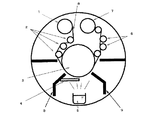
次に、図面に基づいて本発明の金属化プラスティックフィルムを説明する。図1は、本発明のプラスティックフィルム長手方向の金属薄膜表面抵抗(RMD)と幅方向の金属薄膜表面抵抗(RTD)を測定角度で連続的に変化させた金属化プラスティックフィルムを作成する真空蒸着機断面の概略図の例である。
【0013】
図1において、真空蒸着機は、繰り出しロール1から送り出されるプラスティックフィルム8が、プラスティックフィルム8を走行させるために配置された中間ロール2を経て、一部を真空蒸着機の下室にさらされた冷却ロール3上で金属蒸発源5からの蒸発金属がプラスティックフィルム8に蒸着され、巻き取りロール7で巻き取られるようになっている。
【0014】
なお、下室には、必要部分のみプラスティックフィルム8に付着させるために、2枚の隔壁板9が設けられ、さらに必要に応じ、その中で蒸発金属を付着させる範囲制限のための防着板4が配置されており、また上室には金属化プラスティックフィルムを巻き取る前に薄膜金属表面抵抗を測定するために抵抗測定ロール6が設けられている。
【0015】
図1では、蒸発金属の必要部分のみプラスティックフィルム8に付着させるために、防着板4で金属蒸気の選択をしているが、本発明はこれに限定するものでなく、例えば、下室の金属蒸発源5の位置を冷却ロール3の真下からずらし、基材であるプラスティックフィルム8の下室への入り口側、もしくは出口側にずらすことによっても作成可能である。
【0016】
本発明の金属化プラスティックフィルムにおいては、プラスティックフィルムの長手方向の金属膜表面抵抗値(RMD)と該プラスティックフィルムの幅方向の金属膜表面抵抗値(RTD)の比(RMD/RTD)が3/2以上2以下であることが必要である。
【0017】
プラスティックフィルム長手方向の金属膜表面抵抗値(RMD)は、長手方向の長さ500mm、幅25mmの短冊状に金属化プラスティックフィルムを切り出し、また、プラスティックフィルム幅方向の金属膜表面抵抗値(RTD)は、幅方向の長さ500mm、幅25mmの短冊状に金属化プラスティックフィルムを切り出し、それぞれJIS C−2316に準じて長さ500mmの両端間で抵抗値を測定する。蒸着による金属薄膜表面抵抗値制御は難しく、RMDで±20%程度の許容範囲でしか抵抗値制御できないため、RMD/RTDが3/2未満であると、必要な抵抗値を有する金属化プラスティックフィルムを選択することができなくなる。また、RMD/RTDを2より大きくするためには、防着板4により蒸発金属付着を制限する部分の面積を広く取らなくてはならず、生産性の面で効率が悪くなる。
【0018】
長手方向の金属膜表面抵抗値(RMD)は、金属材質によって異なるが、好ましくは0.4Ω/□〜1.5kΩ/□、より好ましくは、2Ω/□〜600Ω/□である。また、幅方向の金属膜表面抵抗値(RTD)は、金属材質によって異なるが、好ましくは0.2Ω/□〜1kΩ/□、より好ましくは、1Ω/□〜400Ω/□である。
【0019】
長手方向と幅方向の金属膜表面抵抗値を上記の比とするためには、冷却ロール3上で蒸発金属をプラスティックフィルム8に付着させるときに、付着させる部分を選択することが必要であり、冷却ロール3上で蒸発金属を付着させる部分の、好ましい範囲は、冷却ロール3の曲率半径、冷却ロール3と金属蒸発源5の位置関係等の真空蒸着機態様によって異なるが、冷却ロール3中心から直下方向を0°で反時計回り方向を正方向とし、円周方向に±20°の部分の内、一部または全部を除く範囲が好ましい。
【0020】
また、本発明の金属化プラスティックフィルムにおいては、プラスティックフィルムの幅方向から角度θ°の向きで切り出した短冊状の金属化プラスティックフィルムの金属膜抵抗値(Rθ)をRTD≦Rθ≦RMDの範囲とすることが好ましい。金属膜抵抗値をこの範囲とすることで、必要な抵抗値選択を容易にすることができる。
【0021】
さらに、本発明の金属化プラスティックフィルムにおいては、プラスティックフィルムの幅方向から角度θ°の向きで切り出した短冊状の金属化プラスティックフィルムの金属膜表面抵抗(Rθ)について、Rθ=RTD+θ°/90×(RMD−RTD)の関係式が成り立っていれば、RMDおよびRTD の値を測定すると、θ°の角度で金属化プラスティックフィルムを切り出すことで、容易に必要な抵抗値を選択することができる。
【0022】
次に、本発明の金属化プラスティックフィルムの製造方法について説明する。
【0023】
基材であるプラスティックフィルムへの導電性金属薄膜の形成方法は、金属蒸発方式として高周波誘導加熱方式や直接加熱方式などを利用した真空蒸着法等がある。
【0024】
本発明の金属化プラスティックフィルムは、電気回路に使用される電気抵抗部品やフィルムコンデンサ等に好適に使用される。
【0025】
【実施例】
以下、本発明の金属化プラスティックフィルムについて実施例により、さらに詳細に説明する。
【0026】
なお、金属膜表面抵抗値の測定に関し、プラスティックフィルム長手方向の金属膜表面抵抗値(RMD)は、長手方向の長さ500mm、幅25mmの短冊状に金属化プラスティックフィルムを切り出し、プラスティックフィルム幅方向の金属膜表面抵抗値(RTD)は、幅方向の長さ500mm、幅25mmの短冊状に金属化プラスティックフィルムを切り出し、JIS C−2316に準じて長さ500mmの両端間で抵抗値を測定した。また、Rθについては、幅方向の角度を0°とし、角度θ方向に長さ500mm、幅25mmの短冊状に金属化プラスティックフィルムを切り出し、同様に測定した。すなわち、Rθ=0°=RTDで、Rθ=90°=RMDである。
【0027】
(実施例1)
冷却ロール3上で蒸着金属(アルミニウム)が付着する面積は2枚の隔壁板9によってプラスティックフィルム8が金属蒸発源5側にさらされる部分(以下、開口部と呼ぶ)によって決まっているが、その面積が約1/2になり、冷却ロール3中心から直下方向を0°で反時計回りを正方向として円周方向に−20°から0°の部分を覆うように防着板4を配置し、厚さ8μmのポリプロピレンフィルム(東レ株式会社製タイプT2372(商品名))に、アルミニウムを抵抗測定ロール6間のアルミニウム金属薄膜抵抗値RMDが約20Ω/□になるように、アルミニウム金属蒸発源の各坩堝1個当たりの投入電力を約8kWにしてフィルム搬送速度を約350m/分で搬送しながら、片面蒸着した。その結果、RMD=20.1Ω/□の金属化プラスティックフィルムが得られた。蒸着中の真空度は、上室で約1Pa、下室で約0.05Pa、高周波誘導加熱坩堝方式の蒸発源を用いて蒸着した。得られた金属化ポリプロピレンフィルムについて、フィルム幅方向から角度をつけて切り出した金属膜抵抗値を表1に示す。
【0028】
(実施例2)
冷却ロール3上で蒸着金属(アルミニウム)が付着する面積が約1/3になり、冷却ロール3中心から直下方向を0°で反時計回りを正方向として円周方向に−20°から20°の部分を覆うように防着板4を配置し、厚さ8μmのポリプロピレンフィルム(東レ株式会社製 タイプT2372(商品名))に、アルミニウムを抵抗測定ロール6間のアルミニウム金属薄膜抵抗値RMDが約20Ω/□になるように、アルミニウム金属蒸発源の各坩堝1個当たりの投入電力を約8kWにしてフィルム搬送速度を約230m/分で搬送しながら、片面蒸着した。蒸着中の真空度は、上室で約1Pa、下室で約0.05Pa、高周波誘導加熱坩堝方式の蒸発源を用いて蒸着した。その結果、RMD=20.0Ω/□の金属化プラスティックフィルムが得られた。得られた金属化ポリプロピレンフィルムについて、フィルム幅方向から角度をつけて切り出した金属膜抵抗値を表1に示す。
【0029】
(実施例3)
冷却ロール3上で蒸着金属(アルミニウム)が付着する面積が約1/3になり、冷却ロール3中心から直下方向を0°で反時計回りを正方向として円周方向に−20°から20°の部分を覆うように防着板4を配置し、厚さ8μmのポリエチレンテレフタレートフィルム(東レ株式会社製 タイプC23(商品名))に、アルミニウムを抵抗測定ロール6間のアルミニウム金属薄膜抵抗値RMDが約20Ω/□になるように、アルミニウム金属蒸発源の各坩堝1個当たりの投入電力を約8kWにしてフィルム搬送速度を約230m/分で搬送しながら、片面蒸着した。蒸着中の真空度は、上室で約1Pa、下室で約0.05Pa、高周波誘導加熱坩堝方式の蒸発源を用いて蒸着した。その結果、RMD=20.0Ω/□の金属化プラスティックフィルムが得られた。得られた金属化ポリエチレンテレフタレートフィルムについて、フィルム幅方向から角度をつけて切り出した金属膜抵抗値を表1に示す。
【0030】
(比較例1)
比較例として、防着板4をはずし、厚さ8μmのポリプロピレンフィルム(東レ株式会社製タイプT2372(商品名))にアルミニウムを抵抗測定ロール6間でアルミニウム金属薄膜抵抗値RMDが約20Ω/□になるように片面蒸着した。その結果、RMD=20.3Ω/□の金属化プラスティックフィルムが得られた。 各々蒸着されたフィルムを、金属化プラスティックフィルムの幅方向を0°とし、時計回りに90°まで、角度15°ごとに、幅25mm、長さ500mmの短冊状にスリットし、薄膜金属抵抗値を測定した。
【0031】
以上の結果を表1に示す。比較例1では角度による金属薄膜表面抵抗の差は1.6Ω/□であったが、実施例1では13.5〜20.1Ω/□、実施例2では10.6〜20.0Ω/□の範囲で抵抗値選択が可能な蒸着フィルムが得られた。また、実施例3では実施例2同様10.7〜20.0Ω/□の範囲で抵抗値選択可能な蒸着フィルムが得られた。
【0032】
上記の結果を表1に示す。
【0033】
【表1】

【発明の効果】
本発明によれば、基材に金属薄膜を形成する真空蒸着法の、表面抵抗値制御問題を解決し、電気回路上必要とされる高精度な金属薄膜表面抵抗を持つ金属化プラスティックフィルムを安定して供給できるようになり、その産業的効果は大である。また、特に、電気・電子部品として使用されるフィルムコンデンサにおいては、本発明の特徴の、プラスティックフィルムの長手方向の金属膜表面抵抗値(RMD)と該プラスティックフィルムの幅方向の金属膜表面抵抗値(RTD)の比(RMD/RTD)が3/2以上2以下であることから、欠陥部破壊時にフィルム長手方向から流れ込む突入電流を制限できると考えられるため、フィルムコンデンサ寿命延命の効果が期待できる。
【図面の簡単な説明】
【図1】図1は、本発明のプラスティックフィルム長手方向の金属薄膜表面抵抗(RMD)と幅方向の金属薄膜表面抵抗(RTD)を測定角度で連続的に変化させた金属化プラスティックフィルムを作成するための真空蒸着機断面の概略図である。
【符号の説明】
1:繰り出しロール
2:中間ロール
3:冷却ロール
4:防着板
5:金属蒸発源
6:抵抗測定ロール
7:巻き取りロール
8:プラスチィックフィルム
9:隔壁板[0001]
TECHNICAL FIELD OF THE INVENTION
The present invention relates to a metallized plastic film suitably used for electric parts, electronic parts and the like, and more particularly to a metallized plastic film suitable for adjusting the resistance value of those electrodes.
[0002]
[Prior art]
2. Description of the Related Art Conventionally, the resistance tolerance of an electric resistance component used in an electric circuit has been required to be very high, such as ± 2% or ± 1%. For example, with respect to electric resistance components, a method of bonding metal foil to a base material to obtain high accuracy and the like are known (see Patent Document 1). Studies have been made to replace these metal foils with vapor-deposited films. However, in the method of forming a metal thin film on a base material by vapor deposition, it is difficult to control the surface resistance of the metal thin film, and the resistance can be controlled only within an allowable range of ± 20% or ± 30%. For this reason, it is difficult to substitute a metal deposition film for an electric resistance component, and it has not been put to practical use.
[0003]
[Patent Document 1]
JP-A-2-88687
[Problems to be solved by the invention]
The problem to be solved by the present invention is to provide a metallized plastic film having extremely high surface resistance required for electric parts and the like.
[0005]
[Means for Solving the Problems]
An object of the present invention is to achieve the above-mentioned object, and a metallized plastic film of the present invention is a metallized plastic film having a conductive metal thin film on both sides or one side of the plastic film; The ratio (R MD / R TD ) of the metal film surface resistance value (R MD ) in the width direction to the metal film surface resistance value (R TD ) in the width direction of the plastic film is 3/2 or more and 2 or less. Metallized plastic film.
[0006]
Further, in the present invention, the metal film surface resistance of the strip-like metallized plastic film cut out in the direction of the angle theta ° from the width direction of the plastic film (R.theta) is, in (a) R TD ≦ Rθ ≦ R MD It is preferable to be a metallized plastic film that can be selected in the range, and (b) a metallized plastic film that satisfies the relational expression of Rθ = R TD + θ ° / 90 × (R MD −R TD ). Included as an embodiment.
[0007]
BEST MODE FOR CARRYING OUT THE INVENTION
Hereinafter, the metallized plastic film of the present invention will be described in detail.
[0008]
The metallized plastic film of the present invention has a basic structure in which a conductive metal thin film is provided on both surfaces or one surface of a plastic film as a base material. Examples of the plastic film preferably used as the substrate in the present invention include films of polyolefin, polyester, polypropylene, polyamide, polyimide, polyphenylene sulfide, polystyrene and the like. Among them, films such as polyethylene terephthalate, polypropylene, and polyphenylene sulfide are particularly preferably used in terms of mechanical properties and electrical properties.
[0009]
The thickness of the plastic film varies depending on the material of the film used, but is preferably 1 to 300 μm, more preferably 1 to 50 μm, and still more preferably 1 to 15 μm.
[0010]
In the metallized plastic film of the present invention, a conductive metal thin film is formed on both surfaces or one surface of the plastic film. Examples of the metal constituting the conductive metal thin film used in the present invention include aluminum, zinc, gold, and silver. It is not particularly limited as long as it has conductivity, such as copper, tin, silicon, magnesium, titanium, nickel, or an alloy thereof, but aluminum, zinc, copper, tin, or an alloy thereof deteriorates. It is particularly preferably used because it is less expensive and less expensive.
[0011]
The thickness of the conductive metal thin film varies depending on the metal material, but is preferably 1 to 100 nm, more preferably 5 to 50 nm.
[0012]
Next, the metallized plastic film of the present invention will be described with reference to the drawings. FIG. 1 shows a vacuum for producing a metallized plastic film in which the metal thin film surface resistance (R MD ) in the longitudinal direction of the plastic film and the metal thin film surface resistance (R TD ) in the width direction of the present invention are continuously changed at a measurement angle. It is an example of the schematic diagram of a vapor deposition machine cross section.
[0013]
In FIG. 1, in the vacuum evaporator, a part of a
[0014]
In the lower chamber, two
[0015]
In FIG. 1, the metal vapor is selected by the deposition-preventing plate 4 so that only the necessary portion of the evaporated metal is adhered to the
[0016]
In the metallized plastic film of the present invention, the ratio (R MD / R TD ) between the metal film surface resistance value (R MD ) in the longitudinal direction of the plastic film and the metal film surface resistance value (R TD ) in the width direction of the plastic film. ) Must be 3/2 or more and 2 or less.
[0017]
The metal film surface resistance value (R MD ) in the longitudinal direction of a plastic film is obtained by cutting a metallized plastic film into a rectangular shape having a length of 500 mm and a width of 25 mm in the longitudinal direction. In TD ), a metallized plastic film is cut into strips having a length of 500 mm in the width direction and a width of 25 mm, and the resistance value is measured between both ends having a length of 500 mm according to JIS C-2316. Deposition difficult metal thin film surface resistivity control by, can not control the resistance value only with a tolerance of about ± 20% in R MD, when R MD / R TD is less than 3/2, the metal having the necessary resistance values It becomes impossible to select a plasticized film. Further, in order to make RMD / RTD larger than 2, it is necessary to increase the area of the portion for restricting the deposition of the evaporated metal by the deposition-preventing plate 4, and the efficiency is lowered in terms of productivity.
[0018]
The surface resistance (R MD ) of the metal film in the longitudinal direction varies depending on the metal material, but is preferably 0.4 Ω / □ to 1.5 kΩ / □, more preferably 2 Ω / □ to 600 Ω / □. Further, the metal film surface resistance value (R TD ) in the width direction varies depending on the metal material, but is preferably from 0.2 Ω / □ to 1 kΩ / □, more preferably from 1 Ω / □ to 400 Ω / □.
[0019]
In order to make the surface resistance value of the metal film in the longitudinal direction and the width direction the above-mentioned ratio, it is necessary to select a portion to be attached when the evaporated metal is attached to the
[0020]
In the metallized plastic films of the present invention, a metal film resistance of the strip-like metallized plastic film cut in a direction from the width direction of the angle theta ° plastic film (R.theta) of R TD ≦ Rθ ≦ R MD It is preferable to set the range. By setting the metal film resistance value in this range, it is possible to easily select a necessary resistance value.
[0021]
Further, in the metallized plastic film of the present invention, the metal film surface resistance (Rθ) of the strip-shaped metallized plastic film cut out at an angle θ ° from the width direction of the plastic film is Rθ = R TD + θ ° / If made up the relational expression 90 × (R MD -R TD) , when measuring the value of R MD and R TD, by cutting the metallized plastic film at an angle of theta °, the easy required resistance You can choose.
[0022]
Next, a method for producing the metallized plastic film of the present invention will be described.
[0023]
As a method for forming a conductive metal thin film on a plastic film as a base material, there is a vacuum evaporation method using a high-frequency induction heating method, a direct heating method, or the like as a metal evaporation method.
[0024]
The metallized plastic film of the present invention is suitably used for electric resistance parts and film capacitors used in electric circuits.
[0025]
【Example】
Hereinafter, the metallized plastic film of the present invention will be described in more detail with reference to examples.
[0026]
Regarding the measurement of the metal film surface resistance value, the metal film surface resistance value (R MD ) in the longitudinal direction of the plastic film is obtained by cutting a metallized plastic film into a strip having a length of 500 mm and a width of 25 mm. The metal film surface resistance (R TD ) in the direction is determined by cutting a metallized plastic film into a rectangular shape having a length of 500 mm and a width of 25 mm in the width direction, and measuring the resistance value between both ends of a length of 500 mm according to JIS C-2316. It was measured. Further, Rθ was measured in the same manner by cutting a metallized plastic film into a rectangular shape having a length of 500 mm and a width of 25 mm in the angle θ direction, with the angle in the width direction being 0 °. That is, in Rθ = 0 ° = R TD, is Rθ = 90 ° = R MD.
[0027]
(Example 1)
The area where the vapor deposition metal (aluminum) adheres on the
[0028]
(Example 2)
The area on the
[0029]
(Example 3)
The area on the
[0030]
(Comparative Example 1)
As a comparative example, remove the deposition preventing plate 4, an aluminum metal film resistance R MD polypropylene film (Toray Co., Ltd. type T2372 (trade name)) of aluminum between the
[0031]
Table 1 shows the above results. In Comparative Example 1, the difference in metal thin film surface resistance depending on the angle was 1.6 Ω / □, but in Example 1 13.5 to 20.1 Ω / □, and in Example 2 10.6 to 20.0 Ω / □. Thus, a vapor-deposited film capable of selecting a resistance value within the range was obtained. Further, in Example 3, as in Example 2, a vapor-deposited film having a selectable resistance value in the range of 10.7 to 20.0 Ω / □ was obtained.
[0032]
Table 1 shows the above results.
[0033]
[Table 1]
【The invention's effect】
According to the present invention, the problem of controlling the surface resistance of the vacuum deposition method of forming a metal thin film on a base material is solved, and a metallized plastic film having a high-precision metal thin film surface resistance required for an electric circuit is stabilized. And the industrial effect is great. Particularly, in a film capacitor used as an electric / electronic component, the metal film surface resistance (R MD ) in the longitudinal direction of the plastic film and the metal film surface resistance in the width direction of the plastic film, which are features of the present invention, are characterized. value since the ratio of (R TD) (R MD / R TD) is 3/2 to 2, it is considered that can limit the inrush current flowing from the longitudinal direction of the film at the time of defect breakdown of the film capacitor life Extension The effect can be expected.
[Brief description of the drawings]
FIG. 1 is a metallized plastic film of the present invention in which the metal thin film surface resistance (R MD ) in the longitudinal direction of the plastic film and the metal thin film surface resistance (R TD ) in the width direction are continuously changed at a measurement angle. FIG. 2 is a schematic view of a cross section of a vacuum deposition machine for producing the slab.
[Explanation of symbols]
1: Feeding roll 2: Intermediate roll 3: Cooling roll 4: Deposition plate 5: Metal evaporation source 6: Resistance measuring roll 7: Winding roll 8: Plastic film 9: Partition plate
Claims (3)
Priority Applications (1)
| Application Number | Priority Date | Filing Date | Title |
|---|---|---|---|
| JP2003027943A JP4304659B2 (en) | 2003-02-05 | 2003-02-05 | Metallized plastic film |
Applications Claiming Priority (1)
| Application Number | Priority Date | Filing Date | Title |
|---|---|---|---|
| JP2003027943A JP4304659B2 (en) | 2003-02-05 | 2003-02-05 | Metallized plastic film |
Publications (2)
| Publication Number | Publication Date |
|---|---|
| JP2004237512A true JP2004237512A (en) | 2004-08-26 |
| JP4304659B2 JP4304659B2 (en) | 2009-07-29 |
Family
ID=32955532
Family Applications (1)
| Application Number | Title | Priority Date | Filing Date |
|---|---|---|---|
| JP2003027943A Expired - Fee Related JP4304659B2 (en) | 2003-02-05 | 2003-02-05 | Metallized plastic film |
Country Status (1)
| Country | Link |
|---|---|
| JP (1) | JP4304659B2 (en) |
Cited By (2)
| Publication number | Priority date | Publication date | Assignee | Title |
|---|---|---|---|---|
| WO2012164903A1 (en) * | 2011-05-30 | 2012-12-06 | パナソニック株式会社 | Metalized film capacitor |
| CN104319095A (en) * | 2014-11-17 | 2015-01-28 | 江苏现代电力科技股份有限公司 | Metallized film for capacitor and manufacturing process thereof |
Families Citing this family (1)
| Publication number | Priority date | Publication date | Assignee | Title |
|---|---|---|---|---|
| JP4818429B2 (en) | 2009-12-28 | 2011-11-16 | 株式会社東芝 | Electronics |
-
2003
- 2003-02-05 JP JP2003027943A patent/JP4304659B2/en not_active Expired - Fee Related
Cited By (3)
| Publication number | Priority date | Publication date | Assignee | Title |
|---|---|---|---|---|
| WO2012164903A1 (en) * | 2011-05-30 | 2012-12-06 | パナソニック株式会社 | Metalized film capacitor |
| US9281123B2 (en) | 2011-05-30 | 2016-03-08 | Panasonic Intellectual Property Management Co., Ltd. | Metalized film capacitor |
| CN104319095A (en) * | 2014-11-17 | 2015-01-28 | 江苏现代电力科技股份有限公司 | Metallized film for capacitor and manufacturing process thereof |
Also Published As
| Publication number | Publication date |
|---|---|
| JP4304659B2 (en) | 2009-07-29 |
Similar Documents
| Publication | Publication Date | Title |
|---|---|---|
| JP5711172B2 (en) | Split sputtering target and manufacturing method thereof | |
| WO2004034412A1 (en) | Metallized film capacitor | |
| JP2005012082A (en) | Metallized film capacitor | |
| JP2004237512A (en) | Metallized plastic film | |
| JP2009000957A (en) | Metal vapor deposition film for capacitor and metallized film capacitor using the same | |
| US10083794B2 (en) | Metallized film capacitor | |
| Wang et al. | Thin film embedded resistors | |
| WO2010044391A1 (en) | Metal foil with electric resistance film and method for manufacturing the metal foil | |
| US10796850B2 (en) | Metalized film and film capacitor | |
| US10640867B2 (en) | Method for manufacturing metallized film | |
| JP2005093373A (en) | Energy device and its manufacturing method | |
| WO1992013352A1 (en) | Chip resistor and chip track bridge | |
| CA1042996A (en) | Windable series-parallel resistance-capacitance network | |
| JP2008263172A (en) | Metallized film and capacitor using the same | |
| JP6600985B2 (en) | Rolled laminated substrate manufacturing method and laminated substrate | |
| JP6281215B2 (en) | Method for forming electric resistance thin film layer and method for producing copper clad laminate | |
| JP2004111192A (en) | Chip type fuse resistor | |
| JP2004158834A (en) | Ceramic laminated body and its manufacture method | |
| JP5373912B2 (en) | Low resistance chip resistor and manufacturing method thereof | |
| JP2015053353A (en) | Deposition method of electric resistance thin film layer and method of manufacturing copper-clad laminate | |
| JP2006019323A (en) | Resistance composition, chip resistor and their manufacturing method | |
| JP6164145B2 (en) | Conductive substrate, method for manufacturing conductive substrate | |
| JP2000012368A (en) | Metallized film capacitor | |
| JP7172334B2 (en) | Apparatus and method for manufacturing resin film substrate with metal film provided with ion beam processing means | |
| JPH0239854B2 (en) |
Legal Events
| Date | Code | Title | Description |
|---|---|---|---|
| A621 | Written request for application examination |
Free format text: JAPANESE INTERMEDIATE CODE: A621 Effective date: 20051215 |
|
| A977 | Report on retrieval |
Effective date: 20080430 Free format text: JAPANESE INTERMEDIATE CODE: A971007 |
|
| A131 | Notification of reasons for refusal |
Effective date: 20080520 Free format text: JAPANESE INTERMEDIATE CODE: A131 |
|
| A131 | Notification of reasons for refusal |
Free format text: JAPANESE INTERMEDIATE CODE: A131 Effective date: 20080902 |
|
| A131 | Notification of reasons for refusal |
Effective date: 20081209 Free format text: JAPANESE INTERMEDIATE CODE: A131 |
|
| TRDD | Decision of grant or rejection written | ||
| A01 | Written decision to grant a patent or to grant a registration (utility model) |
Effective date: 20090414 Free format text: JAPANESE INTERMEDIATE CODE: A01 |
|
| A01 | Written decision to grant a patent or to grant a registration (utility model) |
Free format text: JAPANESE INTERMEDIATE CODE: A01 |
|
| A61 | First payment of annual fees (during grant procedure) |
Free format text: JAPANESE INTERMEDIATE CODE: A61 Effective date: 20090416 |
|
| R150 | Certificate of patent (=grant) or registration of utility model |
Free format text: JAPANESE INTERMEDIATE CODE: R150 |
|
| FPAY | Renewal fee payment (prs date is renewal date of database) |
Free format text: PAYMENT UNTIL: 20120515 Year of fee payment: 3 |
|
| FPAY | Renewal fee payment (prs date is renewal date of database) |
Free format text: PAYMENT UNTIL: 20130515 Year of fee payment: 4 |
|
| LAPS | Cancellation because of no payment of annual fees |