JP2004228281A - Photovoltaic device - Google Patents
Photovoltaic device Download PDFInfo
- Publication number
- JP2004228281A JP2004228281A JP2003013292A JP2003013292A JP2004228281A JP 2004228281 A JP2004228281 A JP 2004228281A JP 2003013292 A JP2003013292 A JP 2003013292A JP 2003013292 A JP2003013292 A JP 2003013292A JP 2004228281 A JP2004228281 A JP 2004228281A
- Authority
- JP
- Japan
- Prior art keywords
- conductive film
- silicon layer
- transparent conductive
- region
- amorphous silicon
- Prior art date
- Legal status (The legal status is an assumption and is not a legal conclusion. Google has not performed a legal analysis and makes no representation as to the accuracy of the status listed.)
- Granted
Links
- 239000000758 substrate Substances 0.000 claims abstract description 65
- 239000004065 semiconductor Substances 0.000 claims description 72
- 229910021417 amorphous silicon Inorganic materials 0.000 abstract description 107
- 229910021421 monocrystalline silicon Inorganic materials 0.000 abstract description 38
- 229910052751 metal Inorganic materials 0.000 description 21
- 239000002184 metal Substances 0.000 description 21
- 238000010248 power generation Methods 0.000 description 19
- 230000015572 biosynthetic process Effects 0.000 description 16
- 238000005215 recombination Methods 0.000 description 12
- 230000006798 recombination Effects 0.000 description 12
- 239000000969 carrier Substances 0.000 description 11
- XUIMIQQOPSSXEZ-UHFFFAOYSA-N Silicon Chemical compound [Si] XUIMIQQOPSSXEZ-UHFFFAOYSA-N 0.000 description 6
- 229910052710 silicon Inorganic materials 0.000 description 6
- 239000010703 silicon Substances 0.000 description 6
- 239000013078 crystal Substances 0.000 description 5
- 229910021419 crystalline silicon Inorganic materials 0.000 description 4
- 238000004519 manufacturing process Methods 0.000 description 4
- BQCADISMDOOEFD-UHFFFAOYSA-N Silver Chemical compound [Ag] BQCADISMDOOEFD-UHFFFAOYSA-N 0.000 description 3
- 230000000694 effects Effects 0.000 description 3
- 238000000034 method Methods 0.000 description 3
- 238000005268 plasma chemical vapour deposition Methods 0.000 description 3
- 229910052709 silver Inorganic materials 0.000 description 3
- 239000004332 silver Substances 0.000 description 3
- 230000007423 decrease Effects 0.000 description 2
- 230000007547 defect Effects 0.000 description 2
- 238000010586 diagram Methods 0.000 description 2
- 239000002019 doping agent Substances 0.000 description 2
- 238000001755 magnetron sputter deposition Methods 0.000 description 2
- 229910021426 porous silicon Inorganic materials 0.000 description 2
- 238000007650 screen-printing Methods 0.000 description 2
- 238000004544 sputter deposition Methods 0.000 description 2
- ZOXJGFHDIHLPTG-UHFFFAOYSA-N Boron Chemical compound [B] ZOXJGFHDIHLPTG-UHFFFAOYSA-N 0.000 description 1
- OAICVXFJPJFONN-UHFFFAOYSA-N Phosphorus Chemical compound [P] OAICVXFJPJFONN-UHFFFAOYSA-N 0.000 description 1
- 229910000577 Silicon-germanium Inorganic materials 0.000 description 1
- 229910052796 boron Inorganic materials 0.000 description 1
- 239000003822 epoxy resin Substances 0.000 description 1
- 238000002474 experimental method Methods 0.000 description 1
- 238000010304 firing Methods 0.000 description 1
- 238000004898 kneading Methods 0.000 description 1
- 239000000463 material Substances 0.000 description 1
- 238000012986 modification Methods 0.000 description 1
- 230000004048 modification Effects 0.000 description 1
- 229910052698 phosphorus Inorganic materials 0.000 description 1
- 239000011574 phosphorus Substances 0.000 description 1
- 229920000647 polyepoxide Polymers 0.000 description 1
- 239000000843 powder Substances 0.000 description 1
Images


Classifications
-
- H01L31/0747—
-
- Y—GENERAL TAGGING OF NEW TECHNOLOGICAL DEVELOPMENTS; GENERAL TAGGING OF CROSS-SECTIONAL TECHNOLOGIES SPANNING OVER SEVERAL SECTIONS OF THE IPC; TECHNICAL SUBJECTS COVERED BY FORMER USPC CROSS-REFERENCE ART COLLECTIONS [XRACs] AND DIGESTS
- Y02—TECHNOLOGIES OR APPLICATIONS FOR MITIGATION OR ADAPTATION AGAINST CLIMATE CHANGE
- Y02E—REDUCTION OF GREENHOUSE GAS [GHG] EMISSIONS, RELATED TO ENERGY GENERATION, TRANSMISSION OR DISTRIBUTION
- Y02E10/00—Energy generation through renewable energy sources
- Y02E10/50—Photovoltaic [PV] energy
Landscapes
- Life Sciences & Earth Sciences (AREA)
- Engineering & Computer Science (AREA)
- Sustainable Energy (AREA)
- Photovoltaic Devices (AREA)
Abstract
Description
【0001】
【発明の属する技術分野】
この発明は、光起電力装置に関し、特に、結晶系半導体基板上に非晶質半導体層が形成された光起電力装置に関する。
【0002】
【従来の技術】
従来、第1導電型の結晶系シリコン基板の表面上に、第2導電型の非晶質シリコン層を形成することによりpn接合が形成される光起電力装置において、第1導電型の結晶系シリコン基板と第2導電型の非晶質シリコン層との間に、実質的に真性な非晶質シリコン層を挿入することにより接合特性を改善したHIT(Heterojunction with intrinsic thin−layer)構造を有する光起電力装置が知られている(たとえば、特許文献1参照)。また、上記のHIT構造を有する光起電力装置において、第1導電型の結晶系シリコン基板の裏面上に、結晶系シリコン基板に近い方から順に、実質的に真性な非晶質シリコン層および第1導電型の非晶質シリコン層がさらに形成された両面HIT構造を有する光起電力装置も知られている。
【0003】
図4は、従来の両面HIT構造を有する光起電力装置の構造を示した断面図である。図5は、図4に示した従来の両面HIT構造を有する光起電力装置の各層の形成領域を示した透視上面図である。図4および図5を参照して、従来の両面HIT構造を有する光起電力装置では、表面側から光が入射されるn型単結晶シリコン基板101の表面上に、実質的に真性なノンドープ非晶質シリコン層102、p型非晶質シリコン層103、ITOからなる透明導電膜104および金属からなる集電極105が順次形成されている。ノンドープ非晶質シリコン層102は、n型単結晶シリコン基板101の表面近傍の結晶欠陥に起因する光誘起キャリアの再結合を抑制する機能を有する。
【0004】
また、n型単結晶シリコン基板101の裏面上には、n型単結晶シリコン基板101に近い方から順に、実質的に真性なノンドープ非晶質シリコン層106、n型非晶質シリコン層107、ITOからなる透明導電膜108および金属からなる集電極109が形成されている。ノンドープ非晶質シリコン層106は、n型単結晶シリコン基板101の裏面近傍の結晶欠陥に起因する光誘起キャリアの再結合を抑制する機能を有する。
【0005】
図4および図5に示した従来の両面HIT構造を有する光起電力装置の製造プロセスとしては、まず、n型単結晶シリコン基板101の表面上に、非晶質シリコン層形成用のメタルマスクを設置する。この後、プラズマCVD法を用いて、n型単結晶シリコン基板101の表面上に、実質的に真性なノンドープ非晶質シリコン層102およびp型非晶質シリコン層103を順次形成する。この後、非晶質シリコン層形成用のメタルマスクを取り外す。次に、p型非晶質シリコン層103上に、透明導電膜形成用のメタルマスクを設置する。この後、スパッタリング法を用いて、p型非晶質シリコン層103上に、ITOからなる透明導電膜104を形成する。この後、透明導電膜形成用のメタルマスクを取り外す。
【0006】
次に、n型単結晶シリコン基板101の裏面上に、非晶質シリコン層形成用のメタルマスクを設置する。この後、プラズマCVD法を用いて、n型単結晶シリコン基板101の裏面上に、n型単結晶シリコン基板101に近い方から順に、実質的に真性なノンドープ非晶質シリコン層106およびn型非晶質シリコン層107を形成する。この後、非晶質シリコン層形成用のメタルマスクを取り外す。次に、n型非晶質シリコン層107上に、透明導電膜形成用のメタルマスクを設置する。この後、スパッタリング法を用いて、n型非晶質シリコン層107上に、ITOからなる透明導電膜108を形成する。この後、透明導電膜形成用のメタルマスクを取り外す。そして、スクリーン印刷法を用いて、透明導電膜104および透明導電膜108上の所定領域に、それぞれ、金属からなる集電極105および集電極109を形成する。
【0007】
ここで、光起電力装置の高出力化のためには、発電領域を規定する表面側の透明導電膜104の形成領域をできる限り大きくすることが望ましい。そのため、表面側の透明導電膜104をノンドープ非晶質シリコン層102およびp型非晶質シリコン層103と実質的に同じ領域にまで拡大して形成することも考えられる。しかしながら、この場合には、表面側の透明導電膜104が、図6に示すように、光起電力装置の側面に回り込みやすくなるので、表面側の透明導電膜104が、裏面側のノンドープ非晶質シリコン層106、n型非晶質シリコン層107および透明導電膜108に接触する場合があるという不都合がある。その結果、リーク電流が発生するとともに、本来意図しない導通経路が形成されるという不都合がある。
【0008】
そこで、図4に示した従来の光起電力装置では、表面側の透明導電膜104が裏面側に回り込むのを抑制するために、表面側の透明導電膜104を、ノンドープ非晶質シリコン層102およびp型非晶質シリコン層103の形成領域よりも小さい領域に形成している。また、表面側の透明導電膜104が裏面側に回り込んだ場合に、表面側の透明導電膜104が裏面側のノンドープ非晶質シリコン層106、n型非晶質シリコン層107および透明導電膜108に接触するのを抑制するために、裏面側のノンドープ非晶質シリコン層106およびn型非晶質シリコン層107を、表面側の透明導電膜104が形成された領域に対応する領域(発電寄与領域)よりも小さい領域に形成するとともに、裏面側の透明導電膜108を、ノンドープ非晶質シリコン層106およびn型非晶質シリコン層107の形成領域よりも小さい領域に形成している。
【0009】
【特許文献1】
特開2001−345463号公報
【0010】
【発明が解決しようとする課題】
しかしながら、図4および図5に示した従来の光起電力装置では、上記したように、表面側の透明導電膜104が裏面側のノンドープ非晶質シリコン層106およびn型非晶質シリコン層107と接触するのを抑制することのみを考慮して、裏面側のノンドープ非晶質シリコン層106およびn型非晶質シリコン層107の形成領域を表面側の透明導電膜104の形成領域よりも小さくしていたため、n型単結晶シリコン基板101の発電寄与領域の裏面側にノンドープ非晶質シリコン層106が形成されていない領域(図4および図5中のAの領域、以下、両面HIT構造未成立領域という)が存在するという不都合があった。その結果、この両面HIT構造未成立領域において光誘起キャリアの再結合が生じるので、光起電力装置の開放電圧および出力が低下するという問題点があった。
【0011】
この発明は、上記のような課題を解決するためになされたものであり、この発明の1つの目的は、高開放電圧および高出力を得ることが可能な光起電力装置を提供することである。
【0012】
この発明のもう1つの目的は、上記の光起電力装置において、リーク電流が発生するのを抑制することである。
【0013】
【課題を解決するための手段および発明の効果】
この発明の一の局面による光起電力装置は、表面および裏面を有し、表面側から光が入射される第1導電型の結晶系半導体基板と、結晶系半導体基板の表面上に形成され、実質的に真性な第1非晶質半導体層と、第1非晶質半導体層上に形成された第2導電型の第2非晶質半導体層と、第2非晶質半導体層上に形成された第1透明導電膜と、結晶系半導体基板の裏面上の、少なくとも第1透明導電膜が形成された領域に対応する領域に形成され、実質的に真性な第3非晶質半導体層とを備えている。なお、本発明における非晶質半導体層は、微結晶半導体層も含む広い概念である。
【0014】
この一の局面による光起電力装置では、上記のように、結晶系半導体基板の裏面上の、少なくとも第1透明導電膜が形成された領域に対応する領域に、実質的に真性な第3非晶質半導体層を設けることによって、少なくとも第1透明導電膜の形成領域に対応する発電寄与領域に第3非晶質半導体層が形成されるので、発電寄与領域での光誘起キャリアの再結合を抑制することができる。その結果、高開放電圧および高出力を得ることができる。
【0015】
上記一の局面による光起電力装置において、好ましくは、実質的に真性な第3非晶質半導体層上に形成された第1導電型の第4非晶質半導体層と、第4非晶質半導体層上に形成された第2透明導電膜とをさらに備えている。このように構成すれば、結晶系半導体基板の表面側および裏面側の両面にHIT構造を有する光起電力装置において、少なくとも第1透明導電膜の形成領域に対応する発電寄与領域に第3非晶質半導体層が形成されるので、発電寄与領域での光誘起キャリアの再結合を抑制することができる。その結果、両面HIT構造を有する光起電力装置において、高開放電圧および高出力を得ることができる。
【0016】
上記一の局面による光起電力装置において、好ましくは、第3非晶質半導体層は、結晶系半導体基板の裏面上の、第1透明導電膜が形成される領域に対応する領域と実質的に同じ領域に形成されている。このように構成すれば、結晶系半導体基板の発電寄与領域での光誘起キャリアの再結合を有効に抑制することが可能な最小限の領域に第3非晶質半導体層が形成されるので、その第3非晶質半導体層によって、発電寄与領域での光誘起キャリアの再結合を抑制しながら、表面側の第1透明導電膜と裏面側の第3非晶質半導体層とが接触するのを抑制することができる。その結果、発電寄与領域での光誘起キャリアの再結合を抑制しながら、表面側の第1透明導電膜から裏面側の第3非晶質半導体層への本来意図しない導通経路が形成されるのを抑制することができる。
【0017】
この場合、好ましくは、第3非晶質半導体層および第4非晶質半導体層は、結晶系半導体基板の裏面上の、第1透明導電膜が形成される領域に対応する領域と実質的に同じ領域に形成されている。このように構成すれば、第3非晶質半導体層の形成時と第4非晶質半導体層の形成時とで、共通のメタルマスクを用いることができるので、製造プロセスを簡略化することができる。
【0018】
上記一の局面による光起電力装置において、好ましくは、第1透明導電膜は、結晶系半導体基板に接触せず、かつ、第1非晶質半導体層が形成された領域よりも小さい領域に形成されており、第2透明導電膜は、結晶系半導体基板に接触せず、かつ、第3非晶質半導体層が形成された領域よりも小さい領域に形成されている。このように構成すれば、表面側の第1透明導電膜の側端部と裏面側の第2透明導電膜の側端部との間の距離を大きくすることができるので、第1透明導電膜および第2透明導電膜の形成時に、表面側の第1透明導電膜と裏面側の第2透明導電膜とが接触するのを抑制することができる。その結果、リーク電流が発生するのを抑制することができる。
【0019】
【発明の実施の形態】
以下、本発明の実施形態を図面に基づいて説明する。
【0020】
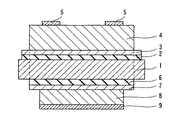
図1は、本発明の一実施形態による光起電力装置の構造を示した断面図である。図2は、図1に示した一実施形態による光起電力装置の各層の形成領域を示した透視上面図である。図1および図2を参照して、本発明の一実施形態による光起電力装置の構造について説明する。
【0021】
本発明の一実施形態による光起電力装置では、図1に示すように、約1Ω・cmの抵抗率と約300μmの厚みとを有するn型(100)単結晶シリコン基板(以下、n型単結晶シリコン基板1という)上に、5nmの厚みを有する実質的に真性なノンドープ非晶質シリコン層2が形成されている。ノンドープ非晶質シリコン層2上には、5nmの厚みを有するp型非晶質シリコン層3が形成されている。ノンドープ非晶質シリコン層2およびp型非晶質シリコン層3は、実質的に同じ領域に形成されているとともに、n型単結晶シリコン基板1の表面領域よりも小さい領域に形成されている。なお、n型単結晶シリコン基板1は、本発明の「結晶系半導体基板」の一例であり、ノンドープ非晶質シリコン層2は、本発明の「第1非晶質半導体層」の一例であり、p型非晶質シリコン層3は、本発明の「第2非晶質半導体層」の一例である。
【0022】
p型非晶質シリコン層3上には、100nmの厚みを有するITO膜からなる透明導電膜4が形成されている。この透明導電膜4は、本発明の「第1透明導電膜」の一例である。透明導電膜4の上面上の所定領域には、図1に示すように、銀(Ag)からなる約10μm〜約30μmの厚みと約100μm〜約500μmの幅とを有する集電極5が形成されている。この集電極5は、所定の間隔を隔てて互いに平行に延びるように形成された複数のフィンガー電極部(図示せず)と、フィンガー電極部に流れる電流を集合させるバスバー電極部(図示せず)とによって構成されている。
【0023】
また、n型単結晶シリコン基板1の裏面上に、5nmの厚みを有する実質的に真性なノンドープ非晶質シリコン層6が形成されている。ノンドープ非晶質シリコン層6上には、5nmの厚みを有するn型非晶質シリコン層7が形成されている。なお、ノンドープ非晶質シリコン層6は、本発明の「第3非晶質半導体層」の一例であり、n型非晶質シリコン層7は、本発明の「第4非晶質半導体層」の一例である。
【0024】
n型非晶質シリコン層7上には、100nmの厚みを有するITO膜からなる透明導電膜8が形成されている。この透明導電膜8は、本発明の「第2透明導電膜」の一例である。透明導電膜8上の所定領域には、約10μm〜約30μmの厚みを有する銀(Ag)からなる集電極9が形成されている。
【0025】
ここで、本実施形態では、図1および図2に示すように、n型単結晶シリコン基板1の裏面上の、透明導電膜4が形成された領域に対応する領域(発電寄与領域)と実質的に同じ領域に、ノンドープ非晶質シリコン層6が形成されている。すなわち、本実施形態では、n型単結晶シリコン基板1の発電寄与領域の裏面側全体が、ノンドープ非晶質シリコン層6によって覆われており、両面HIT構造未成立領域が存在しない構造となっている。また、裏面側のn型非晶質シリコン層7は、ノンドープ非晶質シリコン層6と実質的に同じ領域に形成されている。
【0026】
また、本実施形態では、表面側の透明導電膜4は、n型単結晶シリコン基板1に接触せず、かつ、ノンドープ非晶質シリコン層2およびp型非晶質シリコン層3が形成された領域よりも小さい領域に形成されている。さらに、裏面側の透明導電膜8は、n型単結晶シリコン基板1に接触せず、かつ、ノンドープ非晶質シリコン層6およびn型非晶質シリコン層7が形成された領域よりも小さい領域に形成されている。これにより、表面側の透明導電膜4の側端部と裏面側の透明導電膜8の側端部との間の距離が大きくなるように構成されている。
【0027】
次に、図1を参照して、本発明の一実施形態による光起電力装置の製造プロセスについて説明する。
【0028】
まず、約1Ω・cmの抵抗率と、300μmの厚みとを有するn型単結晶シリコン基板1の表面および裏面を洗浄処理することによって、n型単結晶シリコン基板1の表面および裏面を清浄化する。そして、n型単結晶シリコン基板1の表面上に、非晶質シリコン層形成用のメタルマスクを設置した後、RFプラズマCVD法(13.56MHz)を用いて、n型単結晶シリコン基板1の表面上に、ノンドープ非晶質シリコン層2およびp型非晶質シリコン層3をそれぞれ5nmの厚みで堆積する。この場合の形成条件は、形成温度:約50℃〜約200℃、反応圧力:約5Pa〜約100Pa、RFパワー:約1mW/cm2〜約500mW/cm2である。なお、p型ドーパントとしては、ボロン(B)を用いる。この後、非晶質シリコン層形成用のメタルマスクを取り外す。
【0029】
その後、透明導電膜形成用のメタルマスクをp型非晶質シリコン層3上に設置する。その後、DCマグネトロンスパッタ法を用いて、O2/Ar=約1%、圧力:約0.4Pa〜約1.3Pa、カソードDC電力:約1kWの条件下で、p型非晶質シリコン層3上に、約100nmの厚みを有するITO膜からなる透明導電膜4を形成する。この後、透明導電膜形成用のメタルマスクを取り外す。
【0030】
次に、n型単結晶シリコン基板1の裏面上に非晶質シリコン層形成用のメタルマスクを設置した後、ノンドープ非晶質シリコン層2およびp型非晶質シリコン層3の形成時と同じ形成条件で、RFプラズマCVD法により、n型単結晶シリコン基板1の裏面上に、ノンドープ非晶質シリコン層6およびn型非晶質シリコン層7をそれぞれ5nmの厚みで堆積する。なお、n型ドーパントとしては、燐(P)を用いる。
【0031】
この際、本実施形態では、共通の非晶質シリコン層形成用のメタルマスクを用いて、ノンドープ非晶質シリコン層6およびn型非晶質シリコン層7を、n型単結晶シリコン基板1の裏面上の、表面側の透明導電膜4の形成領域に対応する領域(発電寄与領域)と実質的に同じ領域に形成する。この後、非晶質シリコン層形成用のメタルマスクを取り外す。
【0032】
その後、透明導電膜形成用のメタルマスクをn型非晶質シリコン層7上に設置した後、表面側の透明導電膜4と同じ形成条件で、DCマグネトロンスパッタ法を用いて、n型非晶質シリコン層7上に、約100nmの厚みを有するITO膜からなる裏面側の透明導電膜8を形成する。
【0033】
この後、表面側の透明導電膜4上に、エポキシ樹脂に銀(Ag)微粉末を練り込んだAgペーストをスクリーン印刷法により、約10μm〜約30μmの高さと、約100μm〜約500μmの幅とを有するように形成する。そして、200℃で80分間焼成硬化することによって、所定の間隔を隔てて互いに平行に延びるように形成された複数のフィンガー電極部と、フィンガー電極部に流れる電流を集合させるバスバー電極部とからなる集電極5を形成する。さらに、裏面側の透明導電膜8面上に、Agからなる集電極9を形成する。このようにして、図1に示した本実施形態による光起電力装置が形成される。
【0034】
本実施形態では、上記のように、n型単結晶シリコン基板1の裏面上の、少なくとも表面側の透明導電膜4が形成された領域に対応する領域に、実質的に真性なノンドープ非晶質シリコン層6を設けることによって、少なくとも表面側の透明導電膜4の形成領域に対応する発電寄与領域に裏面側のノンドープ非晶質シリコン層6が形成されるので、発電寄与領域での光誘起キャリアの再結合を抑制することができる。その結果、高開放電圧および高出力を得ることができる。
【0035】
また、本実施形態では、裏面側のノンドープ非晶質シリコン層6を、n型単結晶シリコン基板1の裏面上の、表面側の透明導電膜4が形成される領域に対応する領域と実質的に同じ領域に形成することによって、n型単結晶シリコン基板1の発電寄与領域での光誘起キャリアの再結合を有効に抑制することが可能な最小限の領域にノンドープ非晶質シリコン層6が形成されるので、そのノンドープ非晶質シリコン層6によって、発電寄与領域での光誘起キャリアの再結合を抑制しながら、表面側の透明導電膜4と裏面側のノンドープ非晶質シリコン層6とが接触するのを抑制することができる。その結果、発電寄与領域での光誘起キャリアの再結合を抑制しながら、表面側の透明導電膜4から裏面側のノンドープ非晶質シリコン層6への本来意図しない導通経路が形成されるのを抑制することができる。
【0036】
また、本実施形態では、表面側の透明導電膜4を、n型単結晶シリコン基板1に接触せず、かつ、ノンドープ非晶質シリコン層2が形成された領域よりも小さい領域に形成するとともに、裏面側の透明導電膜8を、n型単結晶シリコン基板1に接触せず、かつ、ノンドープ非晶質シリコン層6が形成された領域よりも小さい領域に形成することによって、表面側の透明導電膜4の側端部と裏面側の透明導電膜8の側端部との間の距離を大きくすることができるので、透明導電膜4および透明導電膜8の形成時に、表面側の透明導電膜4と裏面側の透明導電膜8とが接触するのを抑制することができる。その結果、リーク電流が発生するのを抑制することができる。
【0037】
また、本実施形態では、n型非晶質シリコン層7をノンドープ非晶質シリコン層6と実質的に同じ領域に形成することによって、ノンドープ非晶質シリコン層6の形成時とn型非晶質シリコン層7の形成時とで、共通のメタルマスクを用いることができるので、製造プロセスを簡略化することができる。
【0038】
次に、上記した本実施形態の効果を確認するために行った実験について図3を参照して説明する。図3は、n型単結晶シリコン基板を用いた両面HIT構造を有する光起電力装置における両面HIT構造未成立面積比と規格化出力との関係を示した図である。ここで、両面HIT構造未成立面積比とは、発電面積(表面側の透明導電膜4が形成された面積から表面側の集電極5が形成された面積を差し引いた面積)に対する両面HIT構造未成立領域(図4、図5のA領域参照)の面積比である。また、出力の規格化は、図1および図2に示すような、表面側の透明導電膜4と、裏面側のノンドープ非晶質シリコン層6およびn型非晶質シリコン層7との形成領域が一致している場合(両面HIT構造未成立面積比が0の場合)の光起電力装置の出力により行った。
【0039】
図3から明らかなように、両面HIT構造未成立面積比が増大するのに従って、規格化出力が低下することがわかる。これは、両面HIT構造未成立面積比が増大するのにともなって、開放電圧が低下することに起因すると考えられる。また、図3の結果から、n型単結晶シリコン基板を用いた両面HIT構造を有する光起電力装置において、表面側の透明導電膜の形成領域によって発電寄与領域がほぼ決定される場合に、発電寄与領域の裏面側での光誘起キャリアの再結合防止のためには、発電寄与領域の裏面側にノンドープ非晶質シリコン層が形成されていることが重要であることを確認することができた。
【0040】
なお、今回開示された実施形態は、すべての点で例示であって制限的なものではないと考えられるべきである。本発明の範囲は、上記した実施形態の説明ではなく特許請求の範囲によって示され、さらに特許請求の範囲と均等の意味および範囲内でのすべての変更が含まれる。
【0041】
たとえば、上記実施形態では、表面側および裏面側の両面にHIT構造を有する光起電力装置を例にとって説明したが、本発明はこれに限らず、表面側にのみHIT構造を有する光起電力装置についても本発明は適用可能である。
【0042】
また、上記実施形態では、n型非晶質シリコン層7をノンドープ非晶質シリコン層6の形成領域と実質的に同じ領域となるように形成したが、本発明はこれに限らず、n型非晶質シリコン層をノンドープ非晶質シリコン層の形成領域よりも小さい領域に形成してもよい。
【0043】
また、上記実施形態では、結晶系半導体基板としてn型単結晶シリコン基板を用いたが、本発明はこれに限らず、p型単結晶シリコン基板を用いてもよい。
【0044】
また、上記実施形態では、結晶系半導体基板の上面上および裏面上に形成される非晶質半導体層の一例として、非晶質シリコン層を用いた場合について説明したが、本発明はこれに限らず、非晶質シリコン層に代えて、非晶質SiC層、非晶質SiGe層、非晶質SiOx層、非晶質SiN層などのシリコン系半導体材料からなる非晶質半導体層を用いても同様の効果を得ることができる。
【図面の簡単な説明】
【図1】本発明の一実施形態による光起電力装置の構造を示した断面図である。
【図2】図1に示した一実施形態による光起電力装置の各層の形成領域を示した透視上面図である。
【図3】n型単結晶シリコン基板を用いた両面HIT構造を有する光起電力装置における両面HIT構造未成立面積比と規格化出力との関係を示した図である。
【図4】従来の両面HIT構造を有する光起電力装置の構造を示した断面図である。
【図5】図4に示した従来の両面HIT構造を有する光起電力装置の各層の形成領域を示した透視上面図である。
【図6】図4に示した従来の両面HIT構造を有する光起電力装置において、表面側の透明導電膜の形成領域を大きくした場合の不都合を説明するための断面図である。
【符号の説明】
1 n型単結晶シリコン基板(結晶系半導体基板)
2 ノンドープ非晶質シリコン層(第1非晶質半導体層)
3 p型非晶質シリコン層(第2非晶質半導体層)
4 透明導電膜(第1透明導電膜)
5 集電極
6 ノンドープ非晶質シリコン層(第3非晶質半導体層)
7 n型非晶質シリコン層(第4非晶質半導体層)
8 透明導電膜(第2透明導電膜)
9 集電極[0001]
TECHNICAL FIELD OF THE INVENTION
The present invention relates to a photovoltaic device, and more particularly to a photovoltaic device in which an amorphous semiconductor layer is formed on a crystalline semiconductor substrate.
[0002]
[Prior art]
Conventionally, in a photovoltaic device in which a pn junction is formed by forming a second conductivity type amorphous silicon layer on a surface of a first conductivity type crystal silicon substrate, a first conductivity type crystal silicon substrate is used. A HIT (Heterojunction with intrinsic thin-layer) structure in which a junction property is improved by inserting a substantially intrinsic amorphous silicon layer between the silicon substrate and the second conductivity type amorphous silicon layer. BACKGROUND ART A photovoltaic device is known (for example, see Patent Document 1). Further, in the photovoltaic device having the above-described HIT structure, the substantially intrinsic amorphous silicon layer and the second intrinsic amorphous silicon layer are formed on the back surface of the first conductive type crystalline silicon substrate in order from the one closer to the crystalline silicon substrate. There is also known a photovoltaic device having a double-sided HIT structure in which an amorphous silicon layer of one conductivity type is further formed.
[0003]
FIG. 4 is a sectional view showing the structure of a conventional photovoltaic device having a double-sided HIT structure. FIG. 5 is a transparent top view showing the formation region of each layer of the conventional photovoltaic device having a double-sided HIT structure shown in FIG. Referring to FIGS. 4 and 5, in the conventional photovoltaic device having the double-sided HIT structure, a substantially intrinsic non-doped non-doped layer is formed on the surface of n-type single
[0004]
In addition, on the back surface of the n-type single-
[0005]
As a manufacturing process of the conventional photovoltaic device having the double-sided HIT structure shown in FIGS. 4 and 5, a metal mask for forming an amorphous silicon layer is first formed on the surface of an n-type single
[0006]
Next, a metal mask for forming an amorphous silicon layer is provided on the back surface of the n-type single
[0007]
Here, in order to increase the output of the photovoltaic device, it is desirable to make the formation region of the transparent
[0008]
Therefore, in the conventional photovoltaic device shown in FIG. 4, in order to prevent the transparent
[0009]
[Patent Document 1]
JP 2001-345463 A
[Problems to be solved by the invention]
However, in the conventional photovoltaic device shown in FIGS. 4 and 5, as described above, the transparent
[0011]
SUMMARY OF THE INVENTION The present invention has been made to solve the above problems, and one object of the present invention is to provide a photovoltaic device capable of obtaining a high open-circuit voltage and a high output. .
[0012]
Another object of the present invention is to suppress generation of a leak current in the above-described photovoltaic device.
[0013]
Means for Solving the Problems and Effects of the Invention
A photovoltaic device according to one aspect of the present invention has a front surface and a back surface, a first conductivity type crystalline semiconductor substrate on which light is incident from the front side, and is formed on the surface of the crystalline semiconductor substrate, A substantially intrinsic first amorphous semiconductor layer, a second conductive type second amorphous semiconductor layer formed on the first amorphous semiconductor layer, and a second amorphous semiconductor layer formed on the second amorphous semiconductor layer And a substantially intrinsic third amorphous semiconductor layer formed at least in a region on the back surface of the crystalline semiconductor substrate corresponding to a region where the first transparent conductive film is formed. It has. Note that the amorphous semiconductor layer in the present invention is a broad concept including a microcrystalline semiconductor layer.
[0014]
In the photovoltaic device according to this one aspect, as described above, at least the region corresponding to the region where the first transparent conductive film is formed on the back surface of the crystalline semiconductor substrate is substantially intrinsically non-third. By providing the amorphous semiconductor layer, the third amorphous semiconductor layer is formed at least in the power generation contributing region corresponding to the formation region of the first transparent conductive film. Can be suppressed. As a result, a high open-circuit voltage and a high output can be obtained.
[0015]
In the photovoltaic device according to the one aspect, preferably, the fourth amorphous semiconductor layer of the first conductivity type formed on the substantially intrinsic third amorphous semiconductor layer; A second transparent conductive film formed on the semiconductor layer. According to this structure, in the photovoltaic device having the HIT structure on both the front surface side and the rear surface side of the crystalline semiconductor substrate, at least the third amorphous region is formed in the power generation contributing region corresponding to the formation region of the first transparent conductive film. Since the high quality semiconductor layer is formed, recombination of photoinduced carriers in the power generation contributing region can be suppressed. As a result, a high open-circuit voltage and a high output can be obtained in a photovoltaic device having a double-sided HIT structure.
[0016]
In the photovoltaic device according to the above aspect, the third amorphous semiconductor layer is preferably substantially equal to a region on the back surface of the crystalline semiconductor substrate corresponding to the region where the first transparent conductive film is formed. It is formed in the same area. According to this structure, the third amorphous semiconductor layer is formed in a minimum region where recombination of photoinduced carriers in the power generation contributing region of the crystalline semiconductor substrate can be effectively suppressed. With the third amorphous semiconductor layer, the first transparent conductive film on the front surface and the third amorphous semiconductor layer on the back surface are in contact with each other while suppressing recombination of photoinduced carriers in the power generation contributing region. Can be suppressed. As a result, an unintended conduction path is formed from the first transparent conductive film on the front surface side to the third amorphous semiconductor layer on the rear surface side while suppressing the recombination of photoinduced carriers in the power generation contributing region. Can be suppressed.
[0017]
In this case, preferably, the third amorphous semiconductor layer and the fourth amorphous semiconductor layer substantially correspond to a region on the back surface of the crystalline semiconductor substrate corresponding to the region where the first transparent conductive film is formed. It is formed in the same area. According to this structure, a common metal mask can be used when the third amorphous semiconductor layer is formed and when the fourth amorphous semiconductor layer is formed, so that the manufacturing process can be simplified. it can.
[0018]
In the photovoltaic device according to the one aspect, preferably, the first transparent conductive film is formed in a region not in contact with the crystalline semiconductor substrate and smaller than a region where the first amorphous semiconductor layer is formed. The second transparent conductive film is formed in a region that does not contact the crystalline semiconductor substrate and is smaller than a region where the third amorphous semiconductor layer is formed. According to this structure, the distance between the side end of the first transparent conductive film on the front side and the side end of the second transparent conductive film on the back side can be increased. In addition, when the second transparent conductive film is formed, contact between the first transparent conductive film on the front surface and the second transparent conductive film on the back surface can be suppressed. As a result, generation of a leak current can be suppressed.
[0019]
BEST MODE FOR CARRYING OUT THE INVENTION
Hereinafter, embodiments of the present invention will be described with reference to the drawings.
[0020]
FIG. 1 is a cross-sectional view illustrating a structure of a photovoltaic device according to an embodiment of the present invention. FIG. 2 is a transparent top view showing a formation region of each layer of the photovoltaic device according to the embodiment shown in FIG. The structure of a photovoltaic device according to an embodiment of the present invention will be described with reference to FIGS.
[0021]
In the photovoltaic device according to one embodiment of the present invention, as shown in FIG. 1, an n-type (100) single-crystal silicon substrate (hereinafter, referred to as an n-type single crystal) having a resistivity of about 1 Ω · cm and a thickness of about 300 μm. A substantially intrinsic non-doped
[0022]
On the p-type
[0023]
A substantially intrinsic non-doped
[0024]
On the n-type
[0025]
Here, in the present embodiment, as shown in FIGS. 1 and 2, a region (power generation contributing region) corresponding to the region where the transparent
[0026]
In this embodiment, the transparent
[0027]
Next, a manufacturing process of the photovoltaic device according to one embodiment of the present invention will be described with reference to FIG.
[0028]
First, the front and back surfaces of n-type single-
[0029]
After that, a metal mask for forming a transparent conductive film is provided on the p-type
[0030]
Next, after a metal mask for forming an amorphous silicon layer is provided on the back surface of the n-type single-
[0031]
At this time, in the present embodiment, the non-doped
[0032]
After that, a metal mask for forming a transparent conductive film is provided on the n-type
[0033]
Thereafter, an Ag paste obtained by kneading silver (Ag) fine powder into an epoxy resin is screen-printed on the transparent
[0034]
In the present embodiment, as described above, at least the region corresponding to the region where the transparent
[0035]
Further, in the present embodiment, the non-doped
[0036]
In the present embodiment, the transparent
[0037]
In the present embodiment, the n-type
[0038]
Next, an experiment performed to confirm the effect of the above-described embodiment will be described with reference to FIG. FIG. 3 is a diagram showing the relationship between the ratio of the area where the double-sided HIT structure is not established and the normalized output in a photovoltaic device having a double-sided HIT structure using an n-type single-crystal silicon substrate. Here, the double-sided HIT structure non-established area ratio is defined as the power generation area (the area obtained by subtracting the area in which the front-
[0039]
As is clear from FIG. 3, it is understood that the normalized output decreases as the double-sided HIT structure non-established area ratio increases. This is considered to be due to a decrease in the open-circuit voltage with an increase in the area ratio where the double-sided HIT structure is not established. Also, from the results of FIG. 3, in the photovoltaic device having a double-sided HIT structure using an n-type single crystal silicon substrate, when the power generation contributing region is substantially determined by the formation region of the transparent conductive film on the front surface, It was confirmed that it is important that a non-doped amorphous silicon layer is formed on the back side of the power generation contributing region to prevent recombination of photoinduced carriers on the back side of the contributing region. .
[0040]
It should be noted that the embodiments disclosed this time are illustrative in all aspects and not restrictive. The scope of the present invention is defined by the terms of the claims, rather than the description of the embodiments, and includes all modifications within the scope and meaning equivalent to the terms of the claims.
[0041]
For example, in the above embodiment, the photovoltaic device having the HIT structure on both the front surface side and the rear surface side has been described as an example, but the present invention is not limited to this, and the photovoltaic device having the HIT structure only on the front surface side is described. The present invention is also applicable to
[0042]
In the above embodiment, the n-type
[0043]
In the above embodiment, an n-type single-crystal silicon substrate is used as the crystalline semiconductor substrate. However, the present invention is not limited to this, and a p-type single-crystal silicon substrate may be used.
[0044]
In the above embodiment, the case where the amorphous silicon layer is used as an example of the amorphous semiconductor layer formed on the upper surface and the lower surface of the crystalline semiconductor substrate has been described. However, the present invention is not limited to this. Instead, an amorphous semiconductor layer made of a silicon-based semiconductor material such as an amorphous SiC layer, an amorphous SiGe layer, an amorphous SiO x layer, and an amorphous SiN layer is used instead of the amorphous silicon layer. However, the same effect can be obtained.
[Brief description of the drawings]
FIG. 1 is a cross-sectional view illustrating a structure of a photovoltaic device according to an embodiment of the present invention.
FIG. 2 is a transparent top view showing a formation region of each layer of the photovoltaic device according to the embodiment shown in FIG.
FIG. 3 is a diagram showing a relationship between a double-sided HIT structure non-established area ratio and a normalized output in a photovoltaic device having a double-sided HIT structure using an n-type single-crystal silicon substrate.
FIG. 4 is a cross-sectional view showing the structure of a conventional photovoltaic device having a double-sided HIT structure.
FIG. 5 is a transparent top view showing formation regions of respective layers of the conventional photovoltaic device having a double-sided HIT structure shown in FIG.
FIG. 6 is a cross-sectional view for explaining the inconvenience of a conventional photovoltaic device having a double-sided HIT structure shown in FIG.
[Explanation of symbols]
1 n-type single crystal silicon substrate (crystalline semiconductor substrate)
2 Non-doped amorphous silicon layer (first amorphous semiconductor layer)
3 p-type amorphous silicon layer (second amorphous semiconductor layer)
4 Transparent conductive film (first transparent conductive film)
5
7 n-type amorphous silicon layer (fourth amorphous semiconductor layer)
8 Transparent conductive film (second transparent conductive film)
9 Collector electrode
Claims (5)
前記結晶系半導体基板の表面上に形成され、実質的に真性な第1非晶質半導体層と、
前記第1非晶質半導体層上に形成された第2導電型の第2非晶質半導体層と、
前記第2非晶質半導体層上に形成された第1透明導電膜と、
前記結晶系半導体基板の裏面上の、少なくとも前記第1透明導電膜が形成された領域に対応する領域に形成され、実質的に真性な第3非晶質半導体層とを備えた、光起電力装置。A first-conductivity-type crystalline semiconductor substrate having a front surface and a back surface, to which light is incident from the front surface side;
A substantially intrinsic first amorphous semiconductor layer formed on the surface of the crystalline semiconductor substrate;
A second amorphous semiconductor layer of a second conductivity type formed on the first amorphous semiconductor layer;
A first transparent conductive film formed on the second amorphous semiconductor layer;
A photovoltaic device formed on a back surface of the crystalline semiconductor substrate at least in a region corresponding to a region where the first transparent conductive film is formed, and a substantially intrinsic third amorphous semiconductor layer. apparatus.
前記第4非晶質半導体層上に形成された第2透明導電膜とをさらに備えた、請求項1に記載の光起電力装置。A first conductive type fourth amorphous semiconductor layer formed on the substantially intrinsic third amorphous semiconductor layer;
The photovoltaic device according to claim 1, further comprising a second transparent conductive film formed on the fourth amorphous semiconductor layer.
前記第2透明導電膜は、前記結晶系半導体基板に接触せず、かつ、前記第3非晶質半導体層が形成された領域よりも小さい領域に形成されている、請求項1〜4のいずれか1項に記載の光起電力装置。The first transparent conductive film is formed in a region that does not contact the crystalline semiconductor substrate and is smaller than a region where the first amorphous semiconductor layer is formed;
5. The device according to claim 1, wherein the second transparent conductive film is formed in a region that is not in contact with the crystalline semiconductor substrate and is smaller than a region where the third amorphous semiconductor layer is formed. The photovoltaic device according to claim 1.
Priority Applications (1)
| Application Number | Priority Date | Filing Date | Title |
|---|---|---|---|
| JP2003013292A JP4194379B2 (en) | 2003-01-22 | 2003-01-22 | Photovoltaic device |
Applications Claiming Priority (1)
| Application Number | Priority Date | Filing Date | Title |
|---|---|---|---|
| JP2003013292A JP4194379B2 (en) | 2003-01-22 | 2003-01-22 | Photovoltaic device |
Publications (2)
| Publication Number | Publication Date |
|---|---|
| JP2004228281A true JP2004228281A (en) | 2004-08-12 |
| JP4194379B2 JP4194379B2 (en) | 2008-12-10 |
Family
ID=32901659
Family Applications (1)
| Application Number | Title | Priority Date | Filing Date |
|---|---|---|---|
| JP2003013292A Expired - Fee Related JP4194379B2 (en) | 2003-01-22 | 2003-01-22 | Photovoltaic device |
Country Status (1)
| Country | Link |
|---|---|
| JP (1) | JP4194379B2 (en) |
Cited By (11)
| Publication number | Priority date | Publication date | Assignee | Title |
|---|---|---|---|---|
| EP1696492A1 (en) * | 2005-02-25 | 2006-08-30 | Sanyo Electric Co., Ltd. | Photovoltaic cell |
| JP2006237363A (en) * | 2005-02-25 | 2006-09-07 | Sanyo Electric Co Ltd | Photovoltaic device |
| WO2012105155A1 (en) * | 2011-01-31 | 2012-08-09 | 三洋電機株式会社 | Photoelectric converter and method for producing same |
| EP2549547A1 (en) * | 2010-03-19 | 2013-01-23 | Sanyo Electric Co., Ltd. | Solar cell, solar cell module using solar cell, and manufacturing method for solar cell |
| WO2013171619A1 (en) * | 2012-05-16 | 2013-11-21 | Roth & Rau Ag | Hetero-contact solar cell and method for the production thereof |
| EP2682990A1 (en) * | 2012-07-02 | 2014-01-08 | Roth & Rau AG | Hetero-junction solar cell with edge isolation and method of manufacturing same |
| JP2014041968A (en) * | 2012-08-23 | 2014-03-06 | Mitsubishi Electric Corp | Photovoltaic device and method of manufacturing the same |
| WO2014034677A1 (en) * | 2012-08-29 | 2014-03-06 | 三菱電機株式会社 | Photovoltaic element and method for manufacturing same |
| JP2014093418A (en) * | 2012-11-02 | 2014-05-19 | Mitsubishi Electric Corp | Photovoltaic device and method of manufacturing the same, and photovoltaic module |
| EP3196945A1 (en) * | 2016-01-20 | 2017-07-26 | Lg Electronics Inc. | Solar cell |
| WO2019087590A1 (en) * | 2017-10-30 | 2019-05-09 | 株式会社カネカ | Double-sided electrode type solar cell and solar cell module |
-
2003
- 2003-01-22 JP JP2003013292A patent/JP4194379B2/en not_active Expired - Fee Related
Cited By (26)
| Publication number | Priority date | Publication date | Assignee | Title |
|---|---|---|---|---|
| JP2006237363A (en) * | 2005-02-25 | 2006-09-07 | Sanyo Electric Co Ltd | Photovoltaic device |
| JP4502845B2 (en) * | 2005-02-25 | 2010-07-14 | 三洋電機株式会社 | Photovoltaic element |
| US7781669B2 (en) | 2005-02-25 | 2010-08-24 | Sanyo Electric Co., Ltd. | Photovoltaic cell |
| EP1696492A1 (en) * | 2005-02-25 | 2006-08-30 | Sanyo Electric Co., Ltd. | Photovoltaic cell |
| USRE45872E1 (en) | 2005-02-25 | 2016-01-26 | Panasonic Intellectual Property Management Co., Ltd. | Photovoltaic cell |
| EP2439780A3 (en) * | 2005-02-25 | 2015-05-27 | Sanyo Electric Co., Ltd. | Photovoltaic cell |
| EP2549547A1 (en) * | 2010-03-19 | 2013-01-23 | Sanyo Electric Co., Ltd. | Solar cell, solar cell module using solar cell, and manufacturing method for solar cell |
| EP2549547A4 (en) * | 2010-03-19 | 2014-01-01 | Sanyo Electric Co | Solar cell, solar cell module using solar cell, and manufacturing method for solar cell |
| US9299871B2 (en) | 2010-03-19 | 2016-03-29 | Panasonic Intellectual Property Management Co., Ltd. | Solar cell, solar cell module using solar cell, and manufacturing method for solar cell |
| JPWO2012105155A1 (en) * | 2011-01-31 | 2014-07-03 | 三洋電機株式会社 | Photoelectric conversion device and manufacturing method thereof |
| WO2012105155A1 (en) * | 2011-01-31 | 2012-08-09 | 三洋電機株式会社 | Photoelectric converter and method for producing same |
| WO2013171619A1 (en) * | 2012-05-16 | 2013-11-21 | Roth & Rau Ag | Hetero-contact solar cell and method for the production thereof |
| EP3832737A1 (en) * | 2012-07-02 | 2021-06-09 | Meyer Burger (Germany) GmbH | Hetero-junction solar cell with edge isolation and method of manufacturing same |
| EP2682990A1 (en) * | 2012-07-02 | 2014-01-08 | Roth & Rau AG | Hetero-junction solar cell with edge isolation and method of manufacturing same |
| EP4404282A3 (en) * | 2012-07-02 | 2024-10-23 | Meyer Burger (Germany) GmbH | Method of manufacturing a hetero-junction solar cell |
| JP2014041968A (en) * | 2012-08-23 | 2014-03-06 | Mitsubishi Electric Corp | Photovoltaic device and method of manufacturing the same |
| WO2014034677A1 (en) * | 2012-08-29 | 2014-03-06 | 三菱電機株式会社 | Photovoltaic element and method for manufacturing same |
| JP5908095B2 (en) * | 2012-08-29 | 2016-04-26 | 三菱電機株式会社 | Photovoltaic element and manufacturing method thereof |
| JP2014093418A (en) * | 2012-11-02 | 2014-05-19 | Mitsubishi Electric Corp | Photovoltaic device and method of manufacturing the same, and photovoltaic module |
| CN106997906A (en) * | 2016-01-20 | 2017-08-01 | Lg电子株式会社 | Solar cell |
| CN106997906B (en) * | 2016-01-20 | 2019-08-06 | Lg电子株式会社 | Solar battery |
| EP3544059A1 (en) * | 2016-01-20 | 2019-09-25 | Lg Electronics Inc. | Solar cell |
| EP3196945A1 (en) * | 2016-01-20 | 2017-07-26 | Lg Electronics Inc. | Solar cell |
| JPWO2019087590A1 (en) * | 2017-10-30 | 2020-11-12 | 株式会社カネカ | Double-sided electrode type solar cell and solar cell module |
| WO2019087590A1 (en) * | 2017-10-30 | 2019-05-09 | 株式会社カネカ | Double-sided electrode type solar cell and solar cell module |
| US11404593B2 (en) | 2017-10-30 | 2022-08-02 | Kaneka Corporation | Double-sided electrode type solar cell and solar cell module |
Also Published As
| Publication number | Publication date |
|---|---|
| JP4194379B2 (en) | 2008-12-10 |
Similar Documents
| Publication | Publication Date | Title |
|---|---|---|
| JP5538360B2 (en) | Solar cell manufacturing method and solar cell | |
| EP3170209B1 (en) | Solar cell with interdigitated back contact | |
| JP5461028B2 (en) | Solar cell | |
| JP4502845B2 (en) | Photovoltaic element | |
| JP5518347B2 (en) | Manufacturing method of solar cell | |
| JP2010219527A (en) | Manufacturing method of back contact single heterojunction-type solar battery, and back contact single heterojunction-type solar battery | |
| JP2010518609A (en) | Hybrid silicon solar cell and method of manufacturing the hybrid silicon solar cell | |
| US9761749B2 (en) | Photoelectric conversion device | |
| JP2010087520A (en) | Heterojunction photovoltaic cell with dual doping and method of manufacturing the same | |
| JP2012227281A (en) | Crystalline silicon solar cell | |
| JP4194379B2 (en) | Photovoltaic device | |
| JP7228561B2 (en) | Solar cell manufacturing method | |
| TWI761662B (en) | Manufacturing method of solar cell | |
| JP4169463B2 (en) | Photovoltaic element manufacturing method | |
| JP5645734B2 (en) | Solar cell element | |
| KR20130035876A (en) | Photoelectric conversion device | |
| WO2019181834A1 (en) | Method for producing solar cell, and solar cell | |
| KR101103706B1 (en) | Method for manufacturing of Back junction solar cells | |
| JP4198079B2 (en) | Photovoltaic device manufacturing method | |
| JP7237920B2 (en) | Solar cell manufacturing method | |
| JP7183245B2 (en) | Solar cell manufacturing method | |
| JP2004221142A (en) | Photovoltaic device and its manufacturing method | |
| TWI581447B (en) | Heterojunction solar cell and fabrication method thereof | |
| JP5816800B2 (en) | Manufacturing method of solar cell | |
| JP2005050976A (en) | Photoelectric conversion device |
Legal Events
| Date | Code | Title | Description |
|---|---|---|---|
| A621 | Written request for application examination |
Free format text: JAPANESE INTERMEDIATE CODE: A621 Effective date: 20050107 |
|
| A977 | Report on retrieval |
Free format text: JAPANESE INTERMEDIATE CODE: A971007 Effective date: 20080528 |
|
| A131 | Notification of reasons for refusal |
Free format text: JAPANESE INTERMEDIATE CODE: A131 Effective date: 20080603 |
|
| A521 | Request for written amendment filed |
Free format text: JAPANESE INTERMEDIATE CODE: A523 Effective date: 20080731 |
|
| TRDD | Decision of grant or rejection written | ||
| A01 | Written decision to grant a patent or to grant a registration (utility model) |
Free format text: JAPANESE INTERMEDIATE CODE: A01 Effective date: 20080826 |
|
| A01 | Written decision to grant a patent or to grant a registration (utility model) |
Free format text: JAPANESE INTERMEDIATE CODE: A01 |
|
| A61 | First payment of annual fees (during grant procedure) |
Free format text: JAPANESE INTERMEDIATE CODE: A61 Effective date: 20080922 |
|
| R151 | Written notification of patent or utility model registration |
Ref document number: 4194379 Country of ref document: JP Free format text: JAPANESE INTERMEDIATE CODE: R151 |
|
| FPAY | Renewal fee payment (event date is renewal date of database) |
Free format text: PAYMENT UNTIL: 20111003 Year of fee payment: 3 |
|
| FPAY | Renewal fee payment (event date is renewal date of database) |
Free format text: PAYMENT UNTIL: 20121003 Year of fee payment: 4 |
|
| FPAY | Renewal fee payment (event date is renewal date of database) |
Free format text: PAYMENT UNTIL: 20131003 Year of fee payment: 5 |
|
| LAPS | Cancellation because of no payment of annual fees |