WO2012105155A1 - Photoelectric converter and method for producing same - Google Patents

Photoelectric converter and method for producing same Download PDF

Info

Publication number
WO2012105155A1
WO2012105155A1 PCT/JP2011/080521 JP2011080521W WO2012105155A1 WO 2012105155 A1 WO2012105155 A1 WO 2012105155A1 JP 2011080521 W JP2011080521 W JP 2011080521W WO 2012105155 A1 WO2012105155 A1 WO 2012105155A1
Authority
WO
WIPO (PCT)
Prior art keywords
photoelectric conversion
transparent conductive
film
conductive film
conversion unit
Prior art date
Application number
PCT/JP2011/080521
Other languages
French (fr)
Japanese (ja)
Inventor
知岐 成田
優也 中村
平 茂治
Original Assignee
三洋電機株式会社
Priority date (The priority date is an assumption and is not a legal conclusion. Google has not performed a legal analysis and makes no representation as to the accuracy of the date listed.)
Filing date
Publication date
Application filed by 三洋電機株式会社 filed Critical 三洋電機株式会社
Priority to JP2012555713A priority Critical patent/JPWO2012105155A1/en
Priority to EP11857851.7A priority patent/EP2657978A4/en
Priority to CN2011800664651A priority patent/CN103339734A/en
Publication of WO2012105155A1 publication Critical patent/WO2012105155A1/en
Priority to US13/953,052 priority patent/US20140130857A1/en

Links

Images

Classifications

    • HELECTRICITY
    • H01ELECTRIC ELEMENTS
    • H01LSEMICONDUCTOR DEVICES NOT COVERED BY CLASS H10
    • H01L31/00Semiconductor devices sensitive to infrared radiation, light, electromagnetic radiation of shorter wavelength or corpuscular radiation and specially adapted either for the conversion of the energy of such radiation into electrical energy or for the control of electrical energy by such radiation; Processes or apparatus specially adapted for the manufacture or treatment thereof or of parts thereof; Details thereof
    • H01L31/02Details
    • H01L31/0224Electrodes
    • H01L31/022408Electrodes for devices characterised by at least one potential jump barrier or surface barrier
    • H01L31/022425Electrodes for devices characterised by at least one potential jump barrier or surface barrier for solar cells
    • H01L31/022441Electrode arrangements specially adapted for back-contact solar cells
    • HELECTRICITY
    • H01ELECTRIC ELEMENTS
    • H01LSEMICONDUCTOR DEVICES NOT COVERED BY CLASS H10
    • H01L31/00Semiconductor devices sensitive to infrared radiation, light, electromagnetic radiation of shorter wavelength or corpuscular radiation and specially adapted either for the conversion of the energy of such radiation into electrical energy or for the control of electrical energy by such radiation; Processes or apparatus specially adapted for the manufacture or treatment thereof or of parts thereof; Details thereof
    • H01L31/02Details
    • H01L31/0224Electrodes
    • H01L31/022408Electrodes for devices characterised by at least one potential jump barrier or surface barrier
    • H01L31/022425Electrodes for devices characterised by at least one potential jump barrier or surface barrier for solar cells
    • H01L31/022433Particular geometry of the grid contacts
    • HELECTRICITY
    • H01ELECTRIC ELEMENTS
    • H01LSEMICONDUCTOR DEVICES NOT COVERED BY CLASS H10
    • H01L31/00Semiconductor devices sensitive to infrared radiation, light, electromagnetic radiation of shorter wavelength or corpuscular radiation and specially adapted either for the conversion of the energy of such radiation into electrical energy or for the control of electrical energy by such radiation; Processes or apparatus specially adapted for the manufacture or treatment thereof or of parts thereof; Details thereof
    • H01L31/02Details
    • H01L31/0224Electrodes
    • H01L31/022466Electrodes made of transparent conductive layers, e.g. TCO, ITO layers
    • HELECTRICITY
    • H01ELECTRIC ELEMENTS
    • H01LSEMICONDUCTOR DEVICES NOT COVERED BY CLASS H10
    • H01L31/00Semiconductor devices sensitive to infrared radiation, light, electromagnetic radiation of shorter wavelength or corpuscular radiation and specially adapted either for the conversion of the energy of such radiation into electrical energy or for the control of electrical energy by such radiation; Processes or apparatus specially adapted for the manufacture or treatment thereof or of parts thereof; Details thereof
    • H01L31/04Semiconductor devices sensitive to infrared radiation, light, electromagnetic radiation of shorter wavelength or corpuscular radiation and specially adapted either for the conversion of the energy of such radiation into electrical energy or for the control of electrical energy by such radiation; Processes or apparatus specially adapted for the manufacture or treatment thereof or of parts thereof; Details thereof adapted as photovoltaic [PV] conversion devices
    • H01L31/06Semiconductor devices sensitive to infrared radiation, light, electromagnetic radiation of shorter wavelength or corpuscular radiation and specially adapted either for the conversion of the energy of such radiation into electrical energy or for the control of electrical energy by such radiation; Processes or apparatus specially adapted for the manufacture or treatment thereof or of parts thereof; Details thereof adapted as photovoltaic [PV] conversion devices characterised by at least one potential-jump barrier or surface barrier
    • H01L31/072Semiconductor devices sensitive to infrared radiation, light, electromagnetic radiation of shorter wavelength or corpuscular radiation and specially adapted either for the conversion of the energy of such radiation into electrical energy or for the control of electrical energy by such radiation; Processes or apparatus specially adapted for the manufacture or treatment thereof or of parts thereof; Details thereof adapted as photovoltaic [PV] conversion devices characterised by at least one potential-jump barrier or surface barrier the potential barriers being only of the PN heterojunction type
    • H01L31/0745Semiconductor devices sensitive to infrared radiation, light, electromagnetic radiation of shorter wavelength or corpuscular radiation and specially adapted either for the conversion of the energy of such radiation into electrical energy or for the control of electrical energy by such radiation; Processes or apparatus specially adapted for the manufacture or treatment thereof or of parts thereof; Details thereof adapted as photovoltaic [PV] conversion devices characterised by at least one potential-jump barrier or surface barrier the potential barriers being only of the PN heterojunction type comprising a AIVBIV heterojunction, e.g. Si/Ge, SiGe/Si or Si/SiC solar cells
    • H01L31/0747Semiconductor devices sensitive to infrared radiation, light, electromagnetic radiation of shorter wavelength or corpuscular radiation and specially adapted either for the conversion of the energy of such radiation into electrical energy or for the control of electrical energy by such radiation; Processes or apparatus specially adapted for the manufacture or treatment thereof or of parts thereof; Details thereof adapted as photovoltaic [PV] conversion devices characterised by at least one potential-jump barrier or surface barrier the potential barriers being only of the PN heterojunction type comprising a AIVBIV heterojunction, e.g. Si/Ge, SiGe/Si or Si/SiC solar cells comprising a heterojunction of crystalline and amorphous materials, e.g. heterojunction with intrinsic thin layer or HIT® solar cells; solar cells
    • YGENERAL TAGGING OF NEW TECHNOLOGICAL DEVELOPMENTS; GENERAL TAGGING OF CROSS-SECTIONAL TECHNOLOGIES SPANNING OVER SEVERAL SECTIONS OF THE IPC; TECHNICAL SUBJECTS COVERED BY FORMER USPC CROSS-REFERENCE ART COLLECTIONS [XRACs] AND DIGESTS
    • Y02TECHNOLOGIES OR APPLICATIONS FOR MITIGATION OR ADAPTATION AGAINST CLIMATE CHANGE
    • Y02EREDUCTION OF GREENHOUSE GAS [GHG] EMISSIONS, RELATED TO ENERGY GENERATION, TRANSMISSION OR DISTRIBUTION
    • Y02E10/00Energy generation through renewable energy sources
    • Y02E10/50Photovoltaic [PV] energy

Definitions

  • the present invention relates to a photoelectric conversion device and a manufacturing method thereof.
  • Patent Document 1 discloses a photoelectric conversion device including a photoelectric conversion unit, a light receiving surface electrode provided on a light receiving surface of the photoelectric conversion unit, and a back electrode provided on the back surface of the photoelectric conversion unit.
  • each of the light receiving surface electrode and the back surface electrode includes a plurality of finger electrode portions and a bus bar electrode portion electrically connected to the plurality of finger electrode portions.
  • the metal atoms constituting the metal layer may diffuse into the semiconductor layer of the photoelectric conversion portion and generate a defect level.
  • a defect level may trap carriers generated in the photoelectric conversion unit and cause a decrease in photoelectric conversion efficiency of the photoelectric conversion device.
  • a photoelectric conversion device includes a photoelectric conversion unit, a light receiving surface electrode provided on a light receiving surface of the photoelectric conversion unit, and a back electrode provided on a back surface of the photoelectric conversion unit, and the back electrode is photoelectrically converted.
  • region on a transparent conductive film are characterized by the above-mentioned.
  • a photoelectric conversion unit is prepared, a mask that covers at least a part of an edge region on the photoelectric conversion unit is arranged, and a photoelectric device that excludes the edge region covered by the mask is removed.
  • a transparent conductive film is laminated on a region on the conversion portion, and a metal film is laminated on a region on the transparent conductive film in a state where a mask to which the transparent conductive film is attached is disposed.
  • a photoelectric conversion unit is prepared, a first mask covering at least a part of the edge region on the photoelectric conversion unit is arranged, and the photoelectric conversion unit on the photoelectric conversion unit excluding the edge region covered by the first mask is arranged.
  • a transparent conductive film is laminated on the region, a second mask covering at least a part of the edge region on the transparent conductive film is disposed, and the transparent conductive film excluding the edge region covered with the second mask
  • a metal film may be stacked in the region.
  • the photoelectric conversion device 10 according to the embodiment of the present invention and the manufacturing method thereof will be described in detail with reference to the drawings.
  • the following embodiment is merely an example.
  • the present invention is not limited to the following embodiments.
  • the drawings referred to in the embodiments are schematically described, and the dimensional ratio of an object drawn in the drawings may be different from the dimensional ratio of an actual object.
  • the specific dimensional ratio of the object should be determined in consideration of the following description.
  • FIG. 1 is a view of the photoelectric conversion device 10 as viewed from the light receiving surface side
  • FIG. 2 is a view of the photoelectric conversion device 10 as viewed from the back surface side.
  • the photoelectric conversion device 10 includes a photoelectric conversion unit 20, a light receiving surface electrode 30 provided on the light receiving surface of the photoelectric conversion unit 20, and a back surface provided on the back surface of the photoelectric conversion unit 20.
  • An electrode 40 provided on the back surface of the photoelectric conversion unit 20.
  • the “light receiving surface” means a surface on which light mainly enters from the outside of the apparatus. For example, when a module such as a solar cell is constructed using the photoelectric conversion device 10, more than 50% to 100% of light incident on the device enters from the light receiving surface side.
  • the “back surface” means a surface opposite to the light receiving surface.
  • the photoelectric conversion unit 20 is a member that generates carriers (electrons and holes) by receiving light such as sunlight.
  • carriers generated by the photoelectric conversion unit 20 are collected by the light receiving surface electrode 30 and the back surface electrode 40.
  • the wiring material which is not shown in figure is electrically connected to the light-receiving surface electrode 30 and the back surface electrode 40, and the photoelectric conversion apparatus 10 is modularized, A carrier is taken out as an electrical energy outside.
  • the photoelectric conversion unit 20 includes an n-type single crystal silicon substrate 21 that is a substantially square crystalline semiconductor substrate.
  • the photoelectric conversion unit 20 includes a p-type amorphous silicon film 23 laminated via an i-type amorphous silicon film 22 on the light-receiving surface of an n-type single crystal silicon substrate 21.
  • a transparent conductive film 31 constituting the light receiving surface electrode 30 is laminated on the light receiving surface of the p-type amorphous silicon film 23.
  • a finger electrode part 32 and a bus bar electrode part 33 for collecting electric power generated by the photoelectric conversion part 20 are formed on the transparent conductive film 31.
  • the photoelectric conversion unit 20 includes an n-type amorphous silicon film 25 stacked via an i-type amorphous silicon film 24 on the back surface of the n-type single crystal silicon substrate 21. .
  • a transparent conductive film 41 constituting the back electrode 40 is laminated on the back surface of the n-type amorphous silicon film 25.
  • a metal film 42 for collecting the electric power generated by the photoelectric conversion unit 20 is provided on the transparent conductive film 41.
  • a protruding electrode 43 is provided as a connection portion with the wiring material.
  • the photoelectric conversion unit 20 has a structure in which amorphous semiconductor thin films are stacked on both sides of a crystalline semiconductor substrate.
  • the photoelectric conversion unit 20 includes a p-type amorphous silicon film 23, an i-type other amorphous silicon film 22, an n-type single crystal silicon substrate 21, an i-type amorphous silicon film 24, and an n-type amorphous silicon film.
  • the p-type amorphous silicon film 23 side is the light receiving surface side.
  • the photoelectric conversion unit 20 includes an i-type amorphous silicon film 22 stacked on the entire light-receiving surface of the n-type single crystal silicon substrate 21 and the entire back surface of the n-type single crystal silicon substrate 21. And an i-type amorphous silicon film 24 stacked on each other. Note that the i-type amorphous silicon films 22 and 24 may be stacked leaving the edge regions of the light-receiving surface and the back surface of the n-type single crystal silicon substrate 21.
  • the i-type amorphous silicon films 22 and 24 are intrinsic amorphous silicon thin films and have, for example, the same composition.
  • the photoelectric conversion unit 20 is stacked on the entire back surface of the i-type amorphous silicon film 24 and the p-type amorphous silicon film 23 stacked on the entire light-receiving surface of the i-type amorphous silicon film 22. And an n-type amorphous silicon film 25.
  • Texture structures can be formed on the light receiving surface and the back surface of the photoelectric conversion unit 20 (n-type single crystal silicon substrate 21), respectively.
  • the “texture structure” is an uneven structure that suppresses surface reflection and increases the light absorption amount of the photoelectric conversion unit 20.
  • a pyramid shape (a quadrangular pyramid shape or a quadrangular pyramid shape obtained by performing anisotropic etching on the light receiving surface and the back surface of the n-type single crystal silicon substrate 21 having a (100) plane is used. Can be exemplified.
  • the thickness of the photoelectric conversion unit 20 (the length in the film stacking direction) is, for example, several hundred ⁇ m, and most of the thickness is the thickness of the n-type single crystal silicon substrate 21.
  • the thickness of the amorphous silicon film is, for example, several nm to several tens of nm.
  • the unevenness height of the texture structure is, for example, several ⁇ m. Therefore, the texture structure is also reflected on the light receiving surface and the back surface of the amorphous silicon film.
  • the light-receiving surface electrode 30 includes a transparent conductive film 31, a plurality of finger electrode portions 32, and a plurality of bus bar electrode portions 33.
  • the finger electrode portion 32 and the bus bar electrode portion 33 are electrically connected to each other, and both are formed on the transparent conductive film 31. That is, in the light receiving surface electrode 30, carriers transmitted from the p-type amorphous silicon film 23 through the transparent conductive film 31 are collected by the finger electrode portion 32 and the bus bar electrode portion 33.
  • the wiring material is electrically connected to the bus bar electrode portion 33 and the collected carriers are taken out.
  • the transparent conductive film 31 is made of, for example, a metal oxide such as indium oxide (In 2 O 3 ), zinc oxide (ZnO), tin oxide (SnO 2 ), and titanium oxide (TiO 2 ) having a polycrystalline structure.
  • These metal oxides contain dopants such as tin (Sn), zinc (Zn), tungsten (W), antimony (Sb), titanium (Ti), aluminum (Al), cerium (Ce), and gallium (Ga). It may be doped. The concentration of the dopant can be 0 to 20 wt%.
  • the thickness of the transparent conductive film 31 is, for example, about 50 nm to 200 nm.
  • the transparent conductive film 31 is preferably laminated on the entire light receiving surface of the p-type amorphous silicon film 23 except for the edge region (hereinafter referred to as the edge region A1).
  • the edge region A1 where the transparent conductive film 31 is not laminated is a surface region having a width of about 1 to 2 mm from the end of the light receiving surface of the p-type amorphous silicon film 23, and is provided in an annular shape around the light receiving surface. Is preferred.
  • the finger electrode portion 32 and the bus bar electrode portion 33 are thin wire electrode portions formed of a conductive paste in which conductive particles such as silver (Ag) are dispersed in a binder resin, for example.
  • the finger electrode part 32 and the bus bar electrode part 33 are provided for collecting the electric power generated by the photoelectric conversion part 20 via the transparent conductive film 31.
  • the finger electrode unit 32 is, for example, a band-shaped metal layer formed on the light receiving surface, and is arranged so that power can be collected evenly from the entire photoelectric conversion unit 20.
  • the finger electrode portions 32 are preferably arranged in parallel with each other with a predetermined interval (for example, a width of 100 ⁇ m and an interval of 2 mm).
  • the bus bar electrode portion 33 is provided to further collect and extract the power collected by the finger electrode portion 32.
  • the bus bar electrode portion 33 is, for example, a band-shaped metal layer formed on the light receiving surface, and is disposed so as to cross the finger electrode portion 32 and be electrically connected to the finger electrode portion 32.
  • the bus bar electrode portions 33 can be arranged in parallel with each other with a predetermined interval, for example. At this time, it is preferable that the bus bar electrode portion 33 is set to have a smaller line width than the finger electrode portions 32 and has a larger line width (for example, a width of 1.5 mm, two).
  • the shape of the finger electrode part 32 and the bus-bar electrode part 33 is not limited to what was illustrated here, For example, it can form in various shapes, such as a zigzag shape.
  • the back electrode 40 is composed of a transparent conductive film 41, a metal film 42, and a plurality of protruding electrodes 43.
  • the protruding electrode 43 is a protruding electrode formed on the metal film 42 so as to protrude in the thickness direction of the photoelectric conversion unit 20, and the wiring material is electrically connected when modularized.
  • the protruding electrode 43 can be formed in a band shape on the metal film 42 by, for example, a conductive paste.
  • the protruding electrodes 43 can be arranged in parallel with each other at a predetermined interval, and two protruding electrodes 43 can be arranged along the same direction as the bus bar electrode portion 33.
  • the shape of the protruding electrode 43 is not limited to what was illustrated here, For example, it can form in various shapes, such as a dot shape and a zigzag shape (refer FIG. 7, 8 mentioned later).
  • the transparent conductive film 41 is made of ITO, ZnO, SnO 2 or the like, like the transparent conductive film 31, and functions as a light transmissive electrode portion. Further, as will be described in detail later, the transparent conductive film 41 has a function of preventing direct contact between the photoelectric conversion unit 20 and the metal film 42 and increasing the reflectance by the interaction with the metal film 42.
  • the thickness of the transparent conductive film 31 is preferably about 50 nm to 200 nm, for example, and the texture structure is also reflected on the back surface of the transparent conductive film 31.
  • the transparent conductive film 41 is preferably laminated on the entire back surface area of the n-type amorphous silicon film 25 except the edge area (hereinafter referred to as edge area A2).
  • the edge region A2 where the transparent conductive film 41 is not laminated is a surface region having a width of about 1 to 2 mm from the end of the back surface of the n-type amorphous silicon film 25, and is provided in an annular shape around the back surface. Is preferred.
  • the metal film 42 is a thin film made of a metal material having high light reflectivity and high conductivity.
  • the reflectance of the metal film 42 is preferably high for light in the infrared region.
  • the reflectance of the metal film 42 is preferably higher than the reflectance of the transparent conductive film 41 for at least light in the infrared region.
  • the metal film 42 functions as an electrode part that collects carriers transmitted from the n-type amorphous silicon film 25 through the transparent conductive film 41.
  • the metal film 42 has a function of reflecting the transmitted light that has passed through the photoelectric conversion unit 20 to the light receiving surface side.
  • the thickness of the metal film 42 is preferably so thick that light cannot be transmitted and thin enough to reflect the texture structure on the back surface.
  • the thickness of the metal film 42 is preferably about 0.1 ⁇ m to 5 ⁇ m. If the texture structure is also reflected on the back surface of the metal film 42, an effect of improving the adhesion between the metal film 42 and the protruding electrode 43 can be obtained.
  • Examples of the metal material constituting the metal film 42 include silver (Ag), aluminum (Al), titanium (Ti), rhodium (Rh), copper (Cu), gold (Au), platinum (Pt), nickel ( Examples thereof include metals such as Ni) and chromium (Cr) or alloys containing one or more thereof.
  • the metal material is preferably a material having a high reflectance with respect to light in the infrared region with a wavelength of about 800 nm to 1200 nm, and among the exemplified materials, Ag, Al, Ti, Rh, Cu, Au, or one or more of them are used.
  • An alloy containing Ag, Al, Ti, or an alloy containing one or more thereof is more preferable, and an alloy containing Ag or Ag is particularly preferable.
  • the metal film 42 may be composed of a laminate of a plurality of films made of the above metal materials.
  • a laminate of an Ag film and an Al film can be exemplified, and in this case, the Ag film is preferably disposed on the transparent conductive film 41 side.
  • the metal film 42 is laminated so as to cover substantially the entire area excluding the edge region (hereinafter referred to as edge region A3) on the transparent conductive film 41, and more preferably on the transparent conductive film 41 except the edge region A3. It is laminated to cover the whole.
  • “so as to cover substantially the whole of the transparent conductive film 41 excluding the edge region A3” means a state that can be regarded as covering substantially the whole of the transparent conductive film 41 except for the edge region A3. For example, it includes a state where a part of the metal film 42 laminated on the transparent conductive film 41 is missing. Specifically, a state where 95% or more of the transparent conductive film 41 excluding the edge region A3 is covered with the metal film 42 can be exemplified.
  • the metal film 42 is laminated so as not to cover the n-type amorphous silicon film 25 beyond the transparent conductive film 41 in at least a part of the edge region A3 of the transparent conductive film 41.
  • the metal film 42 may be laminated on a part of the edge region A3.
  • the metal film 42 is laminated so as not to cover the n-type amorphous silicon film 25 beyond the transparent conductive film 41 over the entire periphery of the edge region A3 of the transparent conductive film 41. That is, it is preferable that the metal film 42 is laminated on substantially the entire surface area or the entire surface area except the edge area A3 on the back surface of the transparent conductive film 41.
  • the edge region A3 where the metal film 42 is not laminated is preferably narrow from the viewpoint of reflection of transmitted light and the like.
  • the width of the edge region A3 is preferably 1 nm or more and 5 mm or less from the end of the transparent conductive film 41.
  • the edge region A3 is preferably provided in a ring shape around the back surface of the transparent conductive film 41.
  • the width of the edge region A3 can be confirmed by, for example, cross-sectional observation with a scanning electron microscope (SEM) or a transmission electron microscope (TEM) (an optical microscope or the like can be used when the width is wide). .
  • the metal film 42 When the metal film 42 is in contact with the edge region A2 of the n-type amorphous silicon film 25 beyond at least part of the edge region A3 of the transparent conductive film 41, the metal atoms constituting the metal film 42 in the region are n. There is a problem that a defect level is generated by diffusing into the type amorphous silicon film 25 and carriers are trapped.
  • the metal film 42 is provided so as not to directly touch the back surface of the photoelectric conversion unit 20 via the transparent conductive film 41 between the back surface of the photoelectric conversion unit 20 (n-type amorphous silicon film 25). For this reason, generation
  • the edge region A3 in a ring shape over the entire circumference of the transparent conductive film 41, the metal film 42 and the photoelectric conversion unit 20 (n-type amorphous silicon film 25) are formed on the entire circumference of the photoelectric conversion unit 20. Contact with can be eliminated. Thereby, generation
  • the photoelectric conversion unit 20 has a configuration in which an amorphous silicon film is laminated on a single crystal silicon substrate, the influence of defect levels due to the metal diffused in the amorphous silicon film becomes large. In such a case, the effect by preventing the contact between the photoelectric conversion unit 20 and the metal film 42 becomes remarkable.
  • a metal film 42 is laminated over a wide area on the back side of the photoelectric conversion unit 20 (n-type amorphous silicon film 25). Thereby, the transmitted light that has entered from the light receiving surface and passed through the photoelectric conversion unit 20 can be reflected by the metal film 42 toward the light receiving surface. Therefore, the light absorption rate in the photoelectric conversion unit 20 is improved.
  • the metal film 42 is laminated between the photoelectric conversion unit 20 via the transparent conductive film 41. Thereby, for example, light absorption due to generation of evanescent light is suppressed, and the reflectance of the metal film 42 is increased. A texture structure is also formed on the back surface of the photoelectric conversion unit 20. For this reason, light is scattered on the back surface, and the light is easily confined in the photoelectric conversion unit 20.
  • the transparent conductive film 41 has good adhesion to both the photoelectric conversion unit 20 and the metal film 42. For this reason, the adhesion strength (peeling strength) of the metal film 42 can be improved.
  • the transparent conductive film 41 has a protrusion that covers the side surface of the metal film 42 in the edge region A2.
  • the “side surface” of the metal film 42 means a surface along the thickness direction of the metal film 42.
  • the form which has the said projection part can be obtained by the method shown in below-mentioned FIG.
  • the protrusion has, for example, a width of several nm to several hundred nm and a height (length in the thickness direction) comparable to that of the metal film 42. In such a configuration, the same effect as described above can be obtained.
  • a clean n-type single crystal silicon substrate 21 is placed in a vacuum chamber, and an i-type amorphous silicon film 24 is laminated on the substrate by, for example, plasma CVD (chemical vapor deposition).
  • an n-type amorphous silicon film 25 is stacked on the i-type amorphous silicon film 24.
  • the surface of the n-type single crystal silicon substrate 21 on which the n-type amorphous silicon film 25 is stacked is the back surface.
  • silane gas SiH 4
  • n-type amorphous silicon film 25 for example, silane (SiH 4 ), hydrogen (H 2 ), and phosphine (PH 3 ) are used as source gases.
  • silane (SiH 4 ), hydrogen (H 2 ), and phosphine (PH 3 ) are used as source gases.
  • the i-type amorphous silicon film 24 and the n-type amorphous silicon film 25 are sequentially stacked on the back surface of the n-type single crystal silicon substrate 21.
  • the i-type amorphous silicon film 22 and the p-type amorphous silicon film 23 can also be stacked on the light receiving surface of the n-type single crystal silicon substrate 21 by plasma CVD.
  • diborane B 2 H 6
  • the finger electrode portion 32 and the bus bar electrode portion 33 of the light receiving surface electrode 30 can be formed, for example, by screen-printing a conductive paste on the transparent conductive film 31 in a desired pattern.
  • various sputtering methods, various vapor deposition methods, various plating methods, and the like may be used instead of the screen printing method.
  • the transparent conductive film 31 can be laminated by the same method as the transparent conductive film 41 (described later).
  • the manufacturing process of the back electrode 40 in particular, the lamination process of the transparent conductive film 41 and the metal film 42 will be described in detail.
  • the laminated structure on the light receiving surface side of the n-type single crystal silicon substrate 21 is omitted.
  • the film laminated on the mask 50 is distinguished from the film laminated on the back surface of the n-type amorphous silicon film 25 by attaching “M” to the reference numeral.
  • FIG. 5A shows a state in which a mask 50 is installed on the back surface of the n-type amorphous silicon film 25.
  • the mask 50 is provided so as to cover the edge region A2 on the back surface of the n-type amorphous silicon film 25.
  • a transparent conductive film 41 is laminated on the back surface of the n-type amorphous silicon film 25 provided with the mask 50 by, for example, sputtering.
  • a metal support frame support frame that supports the n-type single crystal silicon substrate 21 from the back surface side can be used.
  • FIG. 5B shows the intermediate body 11 in which the transparent conductive film 41 is laminated on the entire surface region except the edge region A2 on the back surface of the n-type amorphous silicon film 25.
  • the transparent conductive film 41M is also attached to the mask 50.
  • the transparent conductive film 41 ⁇ / b> M is attached not only to the surface 51 of the mask 50 but also to the opening side surface 52.
  • the transparent conductive film 41M attached to the opening side surface 52 has a thickness of, for example, several nm to several hundred nm, and is formed continuously with the transparent conductive film 41.
  • the metal film 42 is laminated
  • FIG. 5 (c) shows the intermediate body 12 in which the metal film 42 is laminated on the entire surface area excluding the edge area A 3 on the back surface of the transparent conductive film 41.
  • the metal film 42M is also stacked on the transparent conductive film 41M attached to the surface 51 and the opening side surface 52. That is, since the transparent conductive film 41M adheres to the side surface 52 of the opening when the metal film 42 is stacked, the metal film 42 is stacked in a surface region smaller than the opening of the mask 50 by the thickness of the transparent conductive film 41M. Is done. That is, the transparent conductive film 41M attached to the opening side surface 52 functions as a mask that covers the edge region A3.
  • the transparent conductive film 41 and the metal film 42 of the back electrode 40 shown in FIG. 3 are obtained.
  • the transparent conductive film 41M and the metal film 42M attached to the mask 50 are removed together with the mask 50.
  • a part of the transparent conductive film 41M adhering to the opening side surface 52 may be left as a protrusion as shown in FIG.
  • the protruding electrode 43 can be formed on the back surface of the metal film 42 by the same method as the bus bar electrode portion 33 (for example, screen printing method, sputtering method, vapor deposition method, plating method, etc.). Alternatively, the protruding electrode 43 may be formed by laminating a plurality of films made of metal or alloy.
  • the lamination process (a, b) of the transparent conductive film 41 is the same as the example shown in FIG. 5, but the lamination process (c, d) of the metal film 42 is different from the example shown in FIG. ing. That is, in the step of laminating the transparent conductive film 41, as shown in FIGS. 6A and 6B, the transparent conductive film 41 is laminated over the entire surface area except for the edge area A2, using a mask 50. On the other hand, in the stacking process of the metal film 42, as shown in FIG. 6C, a second mask 53 covering the edge region A3 on the back surface of the transparent conductive film 41 is used instead of the mask 50.
  • a metal film 42 is laminated on the back surface of the transparent conductive film 41 provided with the second mask 53.
  • the metal film 42 can be laminated on the entire surface area excluding the edge area A3 of the transparent conductive film 41.
  • the width of the edge region A ⁇ b> 3 can be arbitrarily adjusted by changing the size of the opening of the second mask 53.
  • the design of this embodiment can be changed within a range that does not impair the object of the present invention.
  • the photoelectric conversion unit 20 having a structure in which amorphous silicon thin films are stacked on both surfaces of the n-type single crystal silicon substrate 21 is illustrated, but the structure of the photoelectric conversion unit is not limited thereto.
  • the photoelectric conversion unit may have a structure without the i-type amorphous silicon film 24 and the n-type amorphous silicon film 25 or a structure using a semiconductor other than silicon (for example, gallium arsenide).
  • the p-type amorphous silicon film 23 side is described as the light-receiving surface side.
  • the light-receiving surface electrode 30 is provided on the n-type amorphous silicon film 25 to provide an n-type amorphous silicon film.
  • the 25 side may be the light receiving surface side.
  • the light receiving surface electrode 30 includes the bus bar electrode portion 33 and the back surface electrode 40 includes the protruding electrode 43.
  • the light receiving surface electrode 30 or the back surface electrode 40 includes the bus bar electrode portion 33 or the protruding surface. A so-called bus bar-less electrode without the electrode 43 may be used.
  • each protruding electrode 43 has a rectangular shape extending in a direction intersecting the column, but the shape of each electrode is not limited to this.
  • Each protruding electrode 43 may have, for example, a dot shape or a shape having pleated irregularities.
  • the protruding electrodes 43 may be formed in a zigzag shape.
  • various shapes are exemplified for the protruding electrode 43, but the bus bar electrode portion 33 can also have various shapes similarly to the protruding electrode 43.

Abstract

A photoelectric converter (10) is provided with a photoelectric conversion unit (20), a light-receiving-surface electrode (30) provided on the light-receiving surface of the photoelectric conversion unit (20), and a rear-surface electrode (40) provided on the rear surface of the photoelectric conversion unit (20). The rear-surface electrode (40) includes a transparent conductive film (41) layered on the rear surface of the photoelectric conversion unit (20), and a metallic film (42) layered on substantially the entire surface of the transparent conductive film (41) with the exception of an end edge region (A3).

Description

光電変換装置及びその製造方法Photoelectric conversion device and manufacturing method thereof
 本発明は、光電変換装置及びその製造方法に関する。 The present invention relates to a photoelectric conversion device and a manufacturing method thereof.
 特許文献1には、光電変換部と、光電変換部の受光面に設けられた受光面電極と、光電変換部の裏面に設けられた裏面電極とを備える光電変換装置が開示されている。この光電変換装置では、受光面電極及び裏面電極のそれぞれが、複数のフィンガー電極部と、複数のフィンガー電極部に電気的に接続されたバスバー電極部とを備えている。 Patent Document 1 discloses a photoelectric conversion device including a photoelectric conversion unit, a light receiving surface electrode provided on a light receiving surface of the photoelectric conversion unit, and a back electrode provided on the back surface of the photoelectric conversion unit. In this photoelectric conversion device, each of the light receiving surface electrode and the back surface electrode includes a plurality of finger electrode portions and a bus bar electrode portion electrically connected to the plurality of finger electrode portions.
特開2009‐290234号公報JP 2009-290234 A
 太陽電池等の光電変換装置では、赤外領域の光の透過が問題となる。加えて、光電変換部の薄膜化が進むにつれて、他の領域の光の透過も問題となってきた。 In photoelectric conversion devices such as solar cells, transmission of light in the infrared region becomes a problem. In addition, transmission of light in other regions has also become a problem as the photoelectric conversion portion becomes thinner.
 一方、光電変換装置の裏面にバスバー電極部等の金属層を形成すると、金属層を構成する金属原子が光電変換部の半導体層に拡散して欠陥準位を発生させるおそれがある。このような欠陥準位は光電変換部において生成されたキャリアをトラップし、光電変換装置の光電変換効率を低下させる原因となる可能性がある。 On the other hand, when a metal layer such as a bus bar electrode portion is formed on the back surface of the photoelectric conversion device, the metal atoms constituting the metal layer may diffuse into the semiconductor layer of the photoelectric conversion portion and generate a defect level. Such a defect level may trap carriers generated in the photoelectric conversion unit and cause a decrease in photoelectric conversion efficiency of the photoelectric conversion device.
 本発明に係る光電変換装置は、光電変換部と、光電変換部の受光面に設けられた受光面電極と、光電変換部の裏面に設けられた裏面電極とを備え、裏面電極は、光電変換部の裏面に積層された透明導電膜と、透明導電膜上の端縁領域を除いた略全面に積層された金属膜とを含むことを特徴とする。 A photoelectric conversion device according to the present invention includes a photoelectric conversion unit, a light receiving surface electrode provided on a light receiving surface of the photoelectric conversion unit, and a back electrode provided on a back surface of the photoelectric conversion unit, and the back electrode is photoelectrically converted. The transparent conductive film laminated | stacked on the back surface of the part and the metal film laminated | stacked on the substantially whole surface except the edge area | region on a transparent conductive film are characterized by the above-mentioned.
 本発明に係る光電変換装置の製造方法は、光電変換部を用意し、光電変換部上の端縁領域の少なくとも一部を覆うマスクを配置して、マスクによって覆われた端縁領域を除く光電変換部上の領域に透明導電膜を積層し、透明導電膜が付着したマスクを配置した状態で、透明導電膜上の領域に金属膜を積層することを特徴とする。或いは、光電変換部を用意し、光電変換部上の端縁領域の少なくとも一部を覆う第1のマスクを配置して、第1のマスクによって覆われた端縁領域を除く光電変換部上の領域に透明導電膜を積層し、透明導電膜上の端縁領域の少なくとも一部を覆う第2のマスクを配置して、第2のマスクによって覆われた端縁領域を除く透明導電膜上の領域に金属膜を積層してもよい。 In the method for manufacturing a photoelectric conversion device according to the present invention, a photoelectric conversion unit is prepared, a mask that covers at least a part of an edge region on the photoelectric conversion unit is arranged, and a photoelectric device that excludes the edge region covered by the mask is removed. A transparent conductive film is laminated on a region on the conversion portion, and a metal film is laminated on a region on the transparent conductive film in a state where a mask to which the transparent conductive film is attached is disposed. Alternatively, a photoelectric conversion unit is prepared, a first mask covering at least a part of the edge region on the photoelectric conversion unit is arranged, and the photoelectric conversion unit on the photoelectric conversion unit excluding the edge region covered by the first mask is arranged. A transparent conductive film is laminated on the region, a second mask covering at least a part of the edge region on the transparent conductive film is disposed, and the transparent conductive film excluding the edge region covered with the second mask A metal film may be stacked in the region.
 本発明によれば、改善された光電変換効率を有する光電変換装置及びその製造方法を提供することができる。 According to the present invention, it is possible to provide a photoelectric conversion device having improved photoelectric conversion efficiency and a manufacturing method thereof.
本発明の実施形態である光電変換装置を受光面側から見た図である。It is the figure which looked at the photoelectric conversion apparatus which is embodiment of this invention from the light-receiving surface side. 本発明の実施形態である光電変換装置を裏面側から見た図である。It is the figure which looked at the photoelectric conversion apparatus which is embodiment of this invention from the back surface side. 図1,2のB‐B線断面を模式的に示す図である。It is a figure which shows typically the BB line cross section of FIG. 裏面電極の変形例を示す図である。It is a figure which shows the modification of a back surface electrode. 本発明の実施形態である光電変換装置の製造工程の一部を模式的に示す図である。It is a figure which shows typically a part of manufacturing process of the photoelectric conversion apparatus which is embodiment of this invention. 本発明の実施形態である光電変換装置の製造工程の変形例を示す図である。It is a figure which shows the modification of the manufacturing process of the photoelectric conversion apparatus which is embodiment of this invention. 突起電極の変形例を示す図である。It is a figure which shows the modification of a protruding electrode. 突起電極の他の変形例を示す図である。It is a figure which shows the other modification of a protruding electrode.
 以下、図面を用いて、本発明の実施形態である光電変換装置10及びその製造方法を詳細に説明する。なお、以下の実施形態は、単なる例示である。本発明は、以下の実施形態に限定されない。また、実施形態において参照する図面は、模式的に記載されたものであり、図面に描画された物体の寸法比率などは、現実の物体の寸法比率などとは異なる場合がある。具体的な物体の寸法比率等は、以下の説明を参酌して判断されるべきである。 Hereinafter, the photoelectric conversion device 10 according to the embodiment of the present invention and the manufacturing method thereof will be described in detail with reference to the drawings. The following embodiment is merely an example. The present invention is not limited to the following embodiments. The drawings referred to in the embodiments are schematically described, and the dimensional ratio of an object drawn in the drawings may be different from the dimensional ratio of an actual object. The specific dimensional ratio of the object should be determined in consideration of the following description.
 まず初めに、図1~図4を参照して、光電変換装置10の構成を説明する。 First, the configuration of the photoelectric conversion device 10 will be described with reference to FIGS.
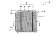
 図1は、光電変換装置10を受光面側から見た図であり、図2は、光電変換装置10を裏面側から見た図である。図1及び図2に示すように、光電変換装置10は、光電変換部20と、光電変換部20の受光面に設けられた受光面電極30と、光電変換部20の裏面に設けられた裏面電極40とを備える。ここで、「受光面」とは、装置の外部から光が主に入射する面を意味する。例えば、光電変換装置10を用いて太陽電池等のモジュールを構築したときに、装置に入射する光のうち50%超過~100%が受光面側から入射する。また、「裏面」とは、受光面と反対側の面を意味する。 FIG. 1 is a view of the photoelectric conversion device 10 as viewed from the light receiving surface side, and FIG. 2 is a view of the photoelectric conversion device 10 as viewed from the back surface side. As shown in FIGS. 1 and 2, the photoelectric conversion device 10 includes a photoelectric conversion unit 20, a light receiving surface electrode 30 provided on the light receiving surface of the photoelectric conversion unit 20, and a back surface provided on the back surface of the photoelectric conversion unit 20. An electrode 40. Here, the “light receiving surface” means a surface on which light mainly enters from the outside of the apparatus. For example, when a module such as a solar cell is constructed using the photoelectric conversion device 10, more than 50% to 100% of light incident on the device enters from the light receiving surface side. The “back surface” means a surface opposite to the light receiving surface.
 光電変換部20は、太陽光等の光を受光することでキャリア(電子及び正孔)を生成する部材である。光電変換装置10では、光電変換部20で生成されたキャリアが受光面電極30及び裏面電極40により収集される。そして、受光面電極30及び裏面電極40に図示しない配線材を電気的に接続して、光電変換装置10をモジュール化することで、キャリアが電気エネルギーとして外部に取り出される。光電変換部20は、略正方形状の結晶系半導体基板であるn型単結晶シリコン基板21を備える。 The photoelectric conversion unit 20 is a member that generates carriers (electrons and holes) by receiving light such as sunlight. In the photoelectric conversion device 10, carriers generated by the photoelectric conversion unit 20 are collected by the light receiving surface electrode 30 and the back surface electrode 40. And the wiring material which is not shown in figure is electrically connected to the light-receiving surface electrode 30 and the back surface electrode 40, and the photoelectric conversion apparatus 10 is modularized, A carrier is taken out as an electrical energy outside. The photoelectric conversion unit 20 includes an n-type single crystal silicon substrate 21 that is a substantially square crystalline semiconductor substrate.
 図1に示すように、n型単結晶シリコン基板21の受光面に、光電変換部20は、i型非晶質シリコン膜22を介して積層されたp型非晶質シリコン膜23を備える。そして、p型非晶質シリコン膜23の受光面に、受光面電極30を構成する透明導電膜31が積層される。さらに、透明導電膜31上には、光電変換部20で発電された電力を集電するためのフィンガー電極部32とバスバー電極部33とが形成される。 As shown in FIG. 1, the photoelectric conversion unit 20 includes a p-type amorphous silicon film 23 laminated via an i-type amorphous silicon film 22 on the light-receiving surface of an n-type single crystal silicon substrate 21. A transparent conductive film 31 constituting the light receiving surface electrode 30 is laminated on the light receiving surface of the p-type amorphous silicon film 23. Furthermore, on the transparent conductive film 31, a finger electrode part 32 and a bus bar electrode part 33 for collecting electric power generated by the photoelectric conversion part 20 are formed.
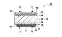
 また、図2に示すように、n型単結晶シリコン基板21の裏面に、光電変換部20は、i型非晶質シリコン膜24を介して積層されたn型非晶質シリコン膜25を備える。そして、n型非晶質シリコン膜25の裏面に、裏面電極40を構成する透明導電膜41が積層される。さらに、透明導電膜41上には、光電変換部20で発電された電力を集電するための金属膜42が設けられる。金属膜42上には、上記配線材との接続部として突起状の突起電極43が設けられる。 In addition, as shown in FIG. 2, the photoelectric conversion unit 20 includes an n-type amorphous silicon film 25 stacked via an i-type amorphous silicon film 24 on the back surface of the n-type single crystal silicon substrate 21. . A transparent conductive film 41 constituting the back electrode 40 is laminated on the back surface of the n-type amorphous silicon film 25. Furthermore, a metal film 42 for collecting the electric power generated by the photoelectric conversion unit 20 is provided on the transparent conductive film 41. On the metal film 42, a protruding electrode 43 is provided as a connection portion with the wiring material.
 つまり、光電変換部20は、結晶系半導体基板の両面に非晶質半導体薄膜が積層された構造を有する。具体的に、光電変換部20は、p型非晶質シリコン膜23,i型他非晶質シリコン膜22,n型単結晶シリコン基板21,i型非晶質シリコン膜24及びn型非晶質シリコン膜25が順に積層された積層構造である。当該積層構造において、p型非晶質シリコン膜23側が受光面側となる。 That is, the photoelectric conversion unit 20 has a structure in which amorphous semiconductor thin films are stacked on both sides of a crystalline semiconductor substrate. Specifically, the photoelectric conversion unit 20 includes a p-type amorphous silicon film 23, an i-type other amorphous silicon film 22, an n-type single crystal silicon substrate 21, an i-type amorphous silicon film 24, and an n-type amorphous silicon film. This is a laminated structure in which quality silicon films 25 are sequentially laminated. In the laminated structure, the p-type amorphous silicon film 23 side is the light receiving surface side.
 以下、図1及び図2に加えて、図3(図1,2のB‐B線断面図)を適宜参照し、光電変換装置10の構成をさらに詳説する。 Hereinafter, in addition to FIG. 1 and FIG. 2, the configuration of the photoelectric conversion device 10 will be described in further detail with reference to FIG.
 図3に示すように、光電変換部20は、n型単結晶シリコン基板21の受光面の全体に積層されたi型非晶質シリコン膜22と、n型単結晶シリコン基板21の裏面の全体に積層されたi型非晶質シリコン膜24とを備える。なお、i型非晶質シリコン膜22,24は、n型単結晶シリコン基板21の受光面、裏面の端縁領域を残して積層されてもよい。i型非晶質シリコン膜22,24は、真性非晶質シリコン薄膜であり、例えば、それぞれ同一の組成を有する。また、光電変換部20は、i型非晶質シリコン膜22の受光面の全体に積層されたp型非晶質シリコン膜23と、i型非晶質シリコン膜24の裏面の全体に積層されたn型非晶質シリコン膜25とを備える。 As shown in FIG. 3, the photoelectric conversion unit 20 includes an i-type amorphous silicon film 22 stacked on the entire light-receiving surface of the n-type single crystal silicon substrate 21 and the entire back surface of the n-type single crystal silicon substrate 21. And an i-type amorphous silicon film 24 stacked on each other. Note that the i-type amorphous silicon films 22 and 24 may be stacked leaving the edge regions of the light-receiving surface and the back surface of the n-type single crystal silicon substrate 21. The i-type amorphous silicon films 22 and 24 are intrinsic amorphous silicon thin films and have, for example, the same composition. In addition, the photoelectric conversion unit 20 is stacked on the entire back surface of the i-type amorphous silicon film 24 and the p-type amorphous silicon film 23 stacked on the entire light-receiving surface of the i-type amorphous silicon film 22. And an n-type amorphous silicon film 25.
 光電変換部20(n型単結晶シリコン基板21)の受光面及び裏面には、それぞれテクスチャ構造(図示せず)を形成することができる。ここで、「テクスチャ構造」とは、表面反射を抑制し、光電変換部20の光吸収量を増大させる凹凸構造である。テクスチャ構造の具体例としては、(100)面を有するn型単結晶シリコン基板21の受光面及び裏面に、異方性エッチングを施すことによって得られるピラミッド状(四角錐状や、四角錐台状)の凹凸構造が例示できる。なお、光電変換部20の厚み(膜の積層方向の長さ)は、例えば、数百μmであり、その大部分がn型単結晶シリコン基板21の厚みである。非晶質シリコン膜の厚みは、例えば、数nm~数十nmである。テクスチャ構造の凹凸高さは、例えば、数μmである。ゆえに、テクスチャ構造は、非晶質シリコン膜の受光面及び裏面にも反映される。 Texture structures (not shown) can be formed on the light receiving surface and the back surface of the photoelectric conversion unit 20 (n-type single crystal silicon substrate 21), respectively. Here, the “texture structure” is an uneven structure that suppresses surface reflection and increases the light absorption amount of the photoelectric conversion unit 20. As a specific example of the texture structure, a pyramid shape (a quadrangular pyramid shape or a quadrangular pyramid shape obtained by performing anisotropic etching on the light receiving surface and the back surface of the n-type single crystal silicon substrate 21 having a (100) plane is used. Can be exemplified. The thickness of the photoelectric conversion unit 20 (the length in the film stacking direction) is, for example, several hundred μm, and most of the thickness is the thickness of the n-type single crystal silicon substrate 21. The thickness of the amorphous silicon film is, for example, several nm to several tens of nm. The unevenness height of the texture structure is, for example, several μm. Therefore, the texture structure is also reflected on the light receiving surface and the back surface of the amorphous silicon film.
 図1及び図3に示すように、受光面電極30は、透明導電膜31と、複数のフィンガー電極部32と、複数のバスバー電極部33とで構成されている。フィンガー電極部32及びバスバー電極部33は、互いに電気的に接続され、いずれも透明導電膜31上に形成されている。即ち、受光面電極30では、p型非晶質シリコン膜23から透明導電膜31を介して伝達されるキャリアがフィンガー電極部32及びバスバー電極部33によって収集される。そして、モジュール化されるときには、上記配線材がバスバー電極部33に電気的に接続されて収集されたキャリアが外部に取り出される。 As shown in FIGS. 1 and 3, the light-receiving surface electrode 30 includes a transparent conductive film 31, a plurality of finger electrode portions 32, and a plurality of bus bar electrode portions 33. The finger electrode portion 32 and the bus bar electrode portion 33 are electrically connected to each other, and both are formed on the transparent conductive film 31. That is, in the light receiving surface electrode 30, carriers transmitted from the p-type amorphous silicon film 23 through the transparent conductive film 31 are collected by the finger electrode portion 32 and the bus bar electrode portion 33. When modularized, the wiring material is electrically connected to the bus bar electrode portion 33 and the collected carriers are taken out.
 透明導電膜31は、例えば、多結晶構造を有する酸化インジウム(In23)、酸化亜鉛(ZnO)、酸化錫(SnO2)、及び酸化チタン(TiO2)等の金属酸化物のうちの少なくとも1つを含む薄膜(TCO膜)であって、光透過性の電極部として機能する。これらの金属酸化物に、錫(Sn)、亜鉛(Zn)、タングステン(W)、アンチモン(Sb)、チタン(Ti)、アルミニウム(Al)、セリウム(Ce)、ガリウム(Ga)などのドーパントがドープされていてもよい。ドーパントの濃度は、0~20wt%とすることができる。透明導電膜31の厚みは、例えば、50nm~200nm程度である。透明導電膜31は、p型非晶質シリコン膜23の受光面において、その端縁領域(以下、端縁領域A1とする)を除く面領域の全体に積層することが好適である。透明導電膜31が積層されない端縁領域A1は、例えば、p型非晶質シリコン膜23の受光面の端から幅1~2mm程度の面領域であって、当該受光面の周囲に環状に設けることが好適である。 The transparent conductive film 31 is made of, for example, a metal oxide such as indium oxide (In 2 O 3 ), zinc oxide (ZnO), tin oxide (SnO 2 ), and titanium oxide (TiO 2 ) having a polycrystalline structure. A thin film (TCO film) including at least one, and functions as a light-transmitting electrode portion. These metal oxides contain dopants such as tin (Sn), zinc (Zn), tungsten (W), antimony (Sb), titanium (Ti), aluminum (Al), cerium (Ce), and gallium (Ga). It may be doped. The concentration of the dopant can be 0 to 20 wt%. The thickness of the transparent conductive film 31 is, for example, about 50 nm to 200 nm. The transparent conductive film 31 is preferably laminated on the entire light receiving surface of the p-type amorphous silicon film 23 except for the edge region (hereinafter referred to as the edge region A1). The edge region A1 where the transparent conductive film 31 is not laminated is a surface region having a width of about 1 to 2 mm from the end of the light receiving surface of the p-type amorphous silicon film 23, and is provided in an annular shape around the light receiving surface. Is preferred.
 フィンガー電極部32及びバスバー電極部33は、例えば、バインダー樹脂中に銀(Ag)等の導電性粒子が分散した導電性ペーストにより形成される細線状の電極部である。フィンガー電極部32及びバスバー電極部33は、透明導電膜31を介して光電変換部20で発電された電力を集電するために設けられる。フィンガー電極部32は、例えば、受光面上に形成された帯状の金属層であり、光電変換部20の全体からまんべんなく電力を集電できるように配置される。フィンガー電極部32は、例えば、所定の間隔をあけて互いに平行に配置することが好適である(例えば、幅100μm、間隔2mm)。 The finger electrode portion 32 and the bus bar electrode portion 33 are thin wire electrode portions formed of a conductive paste in which conductive particles such as silver (Ag) are dispersed in a binder resin, for example. The finger electrode part 32 and the bus bar electrode part 33 are provided for collecting the electric power generated by the photoelectric conversion part 20 via the transparent conductive film 31. The finger electrode unit 32 is, for example, a band-shaped metal layer formed on the light receiving surface, and is arranged so that power can be collected evenly from the entire photoelectric conversion unit 20. For example, the finger electrode portions 32 are preferably arranged in parallel with each other with a predetermined interval (for example, a width of 100 μm and an interval of 2 mm).
 バスバー電極部33は、フィンガー電極部32により集電された電力をさらに集電して取り出すために設けられる。バスバー電極部33は、例えば、受光面上に形成された帯状の金属層であり、フィンガー電極部32と交差してフィンガー電極部32と電気的に接続されるように配置される。バスバー電極部33は、例えば、所定の間隔をあけて互いに平行に配置できる。このとき、バスバー電極部33は、フィンガー電極部32よりも少数で線幅が太く設定されることが好ましい(例えば、幅1.5mm、2本)。なお、フィンガー電極部32及びバスバー電極部33の形状は、ここで例示したものに限定されず、例えば、ジグザグ形状など種々の形状に形成できる。 The bus bar electrode portion 33 is provided to further collect and extract the power collected by the finger electrode portion 32. The bus bar electrode portion 33 is, for example, a band-shaped metal layer formed on the light receiving surface, and is disposed so as to cross the finger electrode portion 32 and be electrically connected to the finger electrode portion 32. The bus bar electrode portions 33 can be arranged in parallel with each other with a predetermined interval, for example. At this time, it is preferable that the bus bar electrode portion 33 is set to have a smaller line width than the finger electrode portions 32 and has a larger line width (for example, a width of 1.5 mm, two). In addition, the shape of the finger electrode part 32 and the bus-bar electrode part 33 is not limited to what was illustrated here, For example, it can form in various shapes, such as a zigzag shape.
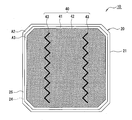
 図2及び図3に示すように、裏面電極40は、透明導電膜41と、金属膜42と、複数の突起電極43とで構成されている。突起電極43は、金属膜42上で光電変換部20の厚み方向に突出して形成された突起状の電極であり、モジュール化されるときに、上記配線材が電気的に接続される。突起電極43は、例えば、導電性ペーストにより、金属膜42上に帯状に形成できる。突起電極43は、例えば、所定の間隔をあけて互いに平行に配置でき、バスバー電極部33と同じ方向に沿って2本配置できる。なお、突起電極43の形状は、ここで例示したものに限定されず、例えば、ドット形状やジグザグ形状など種々の形状に形成できる(後述の図7,8参照)。 2 and 3, the back electrode 40 is composed of a transparent conductive film 41, a metal film 42, and a plurality of protruding electrodes 43. The protruding electrode 43 is a protruding electrode formed on the metal film 42 so as to protrude in the thickness direction of the photoelectric conversion unit 20, and the wiring material is electrically connected when modularized. The protruding electrode 43 can be formed in a band shape on the metal film 42 by, for example, a conductive paste. For example, the protruding electrodes 43 can be arranged in parallel with each other at a predetermined interval, and two protruding electrodes 43 can be arranged along the same direction as the bus bar electrode portion 33. In addition, the shape of the protruding electrode 43 is not limited to what was illustrated here, For example, it can form in various shapes, such as a dot shape and a zigzag shape (refer FIG. 7, 8 mentioned later).
 透明導電膜41は、透明導電膜31と同様に、ITOやZnO、SnO2等からなり、光透過性の電極部として機能する。さらに、透明導電膜41は、詳しくは後述するように、光電変換部20と金属膜42との直接の接触を防止し、金属膜42との相互作用によって反射率を高める機能を有する。透明導電膜31の厚みは、例えば、50nm~200nm程度であることが好ましく、透明導電膜31の裏面にも上記テクスチャ構造が反映される。 The transparent conductive film 41 is made of ITO, ZnO, SnO 2 or the like, like the transparent conductive film 31, and functions as a light transmissive electrode portion. Further, as will be described in detail later, the transparent conductive film 41 has a function of preventing direct contact between the photoelectric conversion unit 20 and the metal film 42 and increasing the reflectance by the interaction with the metal film 42. The thickness of the transparent conductive film 31 is preferably about 50 nm to 200 nm, for example, and the texture structure is also reflected on the back surface of the transparent conductive film 31.
 透明導電膜41は、n型非晶質シリコン膜25の裏面において、その端縁領域(以下、端縁領域A2とする)を除く面領域の全体に積層することが好適である。透明導電膜41が積層されない端縁領域A2は、例えば、n型非晶質シリコン膜25の裏面の端から幅1~2mm程度の面領域であって、当該裏面の周囲に環状に設けることが好適である。 The transparent conductive film 41 is preferably laminated on the entire back surface area of the n-type amorphous silicon film 25 except the edge area (hereinafter referred to as edge area A2). The edge region A2 where the transparent conductive film 41 is not laminated is a surface region having a width of about 1 to 2 mm from the end of the back surface of the n-type amorphous silicon film 25, and is provided in an annular shape around the back surface. Is preferred.
 金属膜42は、光の反射率が高く、且つ高い導電性を有する金属材料からなる薄膜である。金属膜42の反射率は、赤外領域の光に対して高いことが好ましい。金属膜42の反射率は、少なくとも赤外領域の光について、透明導電膜41の反射率よりも高いことが好ましい。金属膜42は、n型非晶質シリコン膜25から透明導電膜41を介して伝達されるキャリアを収集する電極部として機能する。さらに、金属膜42は、光電変換部20を通り抜けた透過光を受光面側に反射する機能を有する。金属膜42の厚みは、光が透過しない程度に厚く、且つ裏面に上記テクスチャ構造が反映可能な程度に薄いことが好ましい。例えば、金属膜42の厚みは、0.1μm~5μm程度であることが好ましい。金属膜42の裏面にもテクスチャ構造が反映されるようにすれば、金属膜42と突起電極43との密着性が良好となる効果も得られる。 The metal film 42 is a thin film made of a metal material having high light reflectivity and high conductivity. The reflectance of the metal film 42 is preferably high for light in the infrared region. The reflectance of the metal film 42 is preferably higher than the reflectance of the transparent conductive film 41 for at least light in the infrared region. The metal film 42 functions as an electrode part that collects carriers transmitted from the n-type amorphous silicon film 25 through the transparent conductive film 41. Furthermore, the metal film 42 has a function of reflecting the transmitted light that has passed through the photoelectric conversion unit 20 to the light receiving surface side. The thickness of the metal film 42 is preferably so thick that light cannot be transmitted and thin enough to reflect the texture structure on the back surface. For example, the thickness of the metal film 42 is preferably about 0.1 μm to 5 μm. If the texture structure is also reflected on the back surface of the metal film 42, an effect of improving the adhesion between the metal film 42 and the protruding electrode 43 can be obtained.
 金属膜42を構成する金属材料としては、例えば、銀(Ag)、アルミニウム(Al)、チタン(Ti)、ロジウム(Rh)、銅(Cu)、金(Au)、白金(Pt)、ニッケル(Ni)、クロム(Cr)などの金属又はそれらの1種以上を含む合金が例示できる。金属材料は、特に波長800nm~1200nm程度の赤外領域の光に対する反射率の高い材料が好ましく、例示した材料の中では、Ag、Al、Ti、Rh、Cu、Au又はそれらの1種以上を含む合金が好ましく、Ag、Al、Ti又はそれらの1種以上を含む合金がより好ましく、Ag又はAgを含む合金が特に好ましい。 Examples of the metal material constituting the metal film 42 include silver (Ag), aluminum (Al), titanium (Ti), rhodium (Rh), copper (Cu), gold (Au), platinum (Pt), nickel ( Examples thereof include metals such as Ni) and chromium (Cr) or alloys containing one or more thereof. The metal material is preferably a material having a high reflectance with respect to light in the infrared region with a wavelength of about 800 nm to 1200 nm, and among the exemplified materials, Ag, Al, Ti, Rh, Cu, Au, or one or more of them are used. An alloy containing Ag, Al, Ti, or an alloy containing one or more thereof is more preferable, and an alloy containing Ag or Ag is particularly preferable.
 金属膜42は、上記金属材料からなる複数の膜の積層体により構成されていてもよい。例えば、Ag膜とAl膜との積層体が例示でき、この場合、Ag膜が透明導電膜41側に配置されることが好ましい。また、Al膜の両面にAg膜が積層されたAg,Al及びAgの積層体、或いはAl膜の代わりに他の金属膜(例えば、Cu膜)を設けたAg,Cu及びAgの積層体であってもよい。 The metal film 42 may be composed of a laminate of a plurality of films made of the above metal materials. For example, a laminate of an Ag film and an Al film can be exemplified, and in this case, the Ag film is preferably disposed on the transparent conductive film 41 side. Also, an Ag, Al, and Ag laminate in which an Ag film is laminated on both sides of an Al film, or an Ag, Cu, and Ag laminate in which another metal film (for example, a Cu film) is provided instead of the Al film. There may be.
 金属膜42は、透明導電膜41上の端縁領域(以下、端縁領域A3とする)を除く略全体を覆うように積層され、より好ましくは、端縁領域A3を除く透明導電膜41上の全体を覆って積層される。ここで、「端縁領域A3を除く透明導電膜41上の略全体を覆うように」とは、端縁領域A3を除く透明導電膜41上の実質的に全体を覆っているとみなせる状態を意味し、例えば、透明導電膜41上に積層された金属膜42の一部が欠けている状態も含む。具体的には、端縁領域A3を除く透明導電膜41上の95%以上を金属膜42が覆っている状態が例示できる。 The metal film 42 is laminated so as to cover substantially the entire area excluding the edge region (hereinafter referred to as edge region A3) on the transparent conductive film 41, and more preferably on the transparent conductive film 41 except the edge region A3. It is laminated to cover the whole. Here, “so as to cover substantially the whole of the transparent conductive film 41 excluding the edge region A3” means a state that can be regarded as covering substantially the whole of the transparent conductive film 41 except for the edge region A3. For example, it includes a state where a part of the metal film 42 laminated on the transparent conductive film 41 is missing. Specifically, a state where 95% or more of the transparent conductive film 41 excluding the edge region A3 is covered with the metal film 42 can be exemplified.
 金属膜42は、透明導電膜41の端縁領域A3の少なくとも一部において、透明導電膜41を超えてn型非晶質シリコン膜25を覆わないように積層される。換言すると、端縁領域A3の一部に金属膜42が積層されてもよい。ただし、好ましくは、透明導電膜41の端縁領域A3の全周に亘って透明導電膜41を超えてn型非晶質シリコン膜25を覆わないように、金属膜42が積層される。即ち、金属膜42は、透明導電膜41の裏面において、その端縁領域A3を除く面領域の略全体又は全体に積層されることが好ましい。 The metal film 42 is laminated so as not to cover the n-type amorphous silicon film 25 beyond the transparent conductive film 41 in at least a part of the edge region A3 of the transparent conductive film 41. In other words, the metal film 42 may be laminated on a part of the edge region A3. However, preferably, the metal film 42 is laminated so as not to cover the n-type amorphous silicon film 25 beyond the transparent conductive film 41 over the entire periphery of the edge region A3 of the transparent conductive film 41. That is, it is preferable that the metal film 42 is laminated on substantially the entire surface area or the entire surface area except the edge area A3 on the back surface of the transparent conductive film 41.
 金属膜42が積層されない端縁領域A3は、透過光の反射等の観点から狭い方が好ましい。例えば、端縁領域A3の幅は、透明導電膜41の端から1nm以上5mm以下とすることが好適である。端縁領域A3は、透明導電膜41の裏面の周囲に環状に設けることが好適である。なお、端縁領域A3の幅は、例えば、走査型電子顕微鏡(SEM)や透過型電子顕微鏡(TEM)による断面観察(幅が広い場合には光学顕微鏡等も使用可能)によって確認することができる。 The edge region A3 where the metal film 42 is not laminated is preferably narrow from the viewpoint of reflection of transmitted light and the like. For example, the width of the edge region A3 is preferably 1 nm or more and 5 mm or less from the end of the transparent conductive film 41. The edge region A3 is preferably provided in a ring shape around the back surface of the transparent conductive film 41. The width of the edge region A3 can be confirmed by, for example, cross-sectional observation with a scanning electron microscope (SEM) or a transmission electron microscope (TEM) (an optical microscope or the like can be used when the width is wide). .
 透明導電膜41の端縁領域A3の少なくとも一部を超えてn型非晶質シリコン膜25の端縁領域A2に金属膜42が接すると、その領域において金属膜42を構成する金属原子がn型非晶質シリコン膜25に拡散して欠陥準位を発生させ、キャリアがトラップされるという問題が生じうる。しかし、金属膜42は、光電変換部20(n型非晶質シリコン膜25)の裏面との間に透明導電膜41を介して、光電変換部20の裏面に直接触れないように設けられる。このため、欠陥順位の発生を抑制できる。好ましくは、端縁領域A3を透明導電膜41の全周に亘って環状に設けることによって、光電変換部20の全周において金属膜42と光電変換部20(n型非晶質シリコン膜25)との接触を無くすことができる。これにより、欠陥準位の発生をより抑制することができる。 When the metal film 42 is in contact with the edge region A2 of the n-type amorphous silicon film 25 beyond at least part of the edge region A3 of the transparent conductive film 41, the metal atoms constituting the metal film 42 in the region are n. There is a problem that a defect level is generated by diffusing into the type amorphous silicon film 25 and carriers are trapped. However, the metal film 42 is provided so as not to directly touch the back surface of the photoelectric conversion unit 20 via the transparent conductive film 41 between the back surface of the photoelectric conversion unit 20 (n-type amorphous silicon film 25). For this reason, generation | occurrence | production of a defect order | rank can be suppressed. Preferably, by providing the edge region A3 in a ring shape over the entire circumference of the transparent conductive film 41, the metal film 42 and the photoelectric conversion unit 20 (n-type amorphous silicon film 25) are formed on the entire circumference of the photoelectric conversion unit 20. Contact with can be eliminated. Thereby, generation | occurrence | production of a defect level can be suppressed more.
 光電変換部20が単結晶シリコン基板上に非晶質シリコン膜を積層した構成を有する場合、非晶質シリコン膜に拡散した金属による欠陥準位の影響が大きくなる。このような場合、光電変換部20と金属膜42との接触を防ぐことによる効果が顕著となる。 When the photoelectric conversion unit 20 has a configuration in which an amorphous silicon film is laminated on a single crystal silicon substrate, the influence of defect levels due to the metal diffused in the amorphous silicon film becomes large. In such a case, the effect by preventing the contact between the photoelectric conversion unit 20 and the metal film 42 becomes remarkable.
 光電変換部20(n型非晶質シリコン膜25)の裏面側の広範囲に金属膜42が積層されている。これにより、受光面から入射して光電変換部20を通り抜けた透過光を金属膜42により受光面側に反射させることができる。ゆえに、光電変換部20における光吸収率が向上する。 A metal film 42 is laminated over a wide area on the back side of the photoelectric conversion unit 20 (n-type amorphous silicon film 25). Thereby, the transmitted light that has entered from the light receiving surface and passed through the photoelectric conversion unit 20 can be reflected by the metal film 42 toward the light receiving surface. Therefore, the light absorption rate in the photoelectric conversion unit 20 is improved.
 金属膜42は、光電変換部20との間に透明導電膜41を介して積層されている。これにより、例えば、エバネッセント光の発生による光の吸収が抑制されて金属膜42の反射率が高まる。なお、光電変換部20の裏面にもテクスチャ構造が形成されている。このため、裏面で光が散乱して光電変換部20内に光が閉じ込められ易くなる。 The metal film 42 is laminated between the photoelectric conversion unit 20 via the transparent conductive film 41. Thereby, for example, light absorption due to generation of evanescent light is suppressed, and the reflectance of the metal film 42 is increased. A texture structure is also formed on the back surface of the photoelectric conversion unit 20. For this reason, light is scattered on the back surface, and the light is easily confined in the photoelectric conversion unit 20.
 透明導電膜41は光電変換部20及び金属膜42のいずれに対しても良好な密着性を有する。このため、金属膜42の密着強度(剥離強度)を向上させることができる。 The transparent conductive film 41 has good adhesion to both the photoelectric conversion unit 20 and the metal film 42. For this reason, the adhesion strength (peeling strength) of the metal film 42 can be improved.
 これらの作用によって、本実施の形態における光電変換装置10では、光電変換効率を向上させることができる。 These actions can improve the photoelectric conversion efficiency in the photoelectric conversion device 10 according to the present embodiment.
 図4に示すように、金属膜42は、その側面の少なくとも一部が透明導電膜41に囲まれていてもよい。即ち、透明導電膜41は、端縁領域A2に、金属膜42の側面を覆う突起部を有している。ここで、金属膜42の「側面」とは、金属膜42の厚み方向に沿った面を意味する。当該突起部を有する形態は、例えば、後述の図5に示す方法により得ることができる。突起部は、例えば、数nm~数百nmの幅と、金属膜42と同程度の高さ(厚み方向の長さ)とを有する。このような構成において、上記と同様の効果を得ることができる。 As shown in FIG. 4, at least a part of the side surface of the metal film 42 may be surrounded by the transparent conductive film 41. That is, the transparent conductive film 41 has a protrusion that covers the side surface of the metal film 42 in the edge region A2. Here, the “side surface” of the metal film 42 means a surface along the thickness direction of the metal film 42. The form which has the said projection part can be obtained by the method shown in below-mentioned FIG. The protrusion has, for example, a width of several nm to several hundred nm and a height (length in the thickness direction) comparable to that of the metal film 42. In such a configuration, the same effect as described above can be obtained.
 次に、上記構成を備える光電変換装置10の製造方法を例示する。 Next, a method for manufacturing the photoelectric conversion device 10 having the above configuration will be exemplified.
 まず、清浄なn型単結晶シリコン基板21を真空チャンバ内に設置し、例えば、プラズマCVD(化学気相成長法)法により、当該基板上にi型非晶質シリコン膜24を積層する。続いて、i型非晶質シリコン膜24上にn型非晶質シリコン膜25を積層する。なお、本実施形態では、n型非晶質シリコン膜25が積層されるn型単結晶シリコン基板21の面が裏面となる。i型非晶質シリコン膜24の積層工程では、例えば、シランガス(SiH4)が原料ガスとして使用される。また、n型非晶質シリコン膜25の積層工程では、例えば、シラン(SiH4)、水素(H2)、及びホスフィン(PH3)が原料ガスとして使用される。このようにして、n型単結晶シリコン基板21の裏面に、i型非晶質シリコン膜24及びn型非晶質シリコン膜25が順に積層される。 First, a clean n-type single crystal silicon substrate 21 is placed in a vacuum chamber, and an i-type amorphous silicon film 24 is laminated on the substrate by, for example, plasma CVD (chemical vapor deposition). Subsequently, an n-type amorphous silicon film 25 is stacked on the i-type amorphous silicon film 24. In the present embodiment, the surface of the n-type single crystal silicon substrate 21 on which the n-type amorphous silicon film 25 is stacked is the back surface. In the lamination process of the i-type amorphous silicon film 24, for example, silane gas (SiH 4 ) is used as a source gas. In the step of laminating the n-type amorphous silicon film 25, for example, silane (SiH 4 ), hydrogen (H 2 ), and phosphine (PH 3 ) are used as source gases. In this way, the i-type amorphous silicon film 24 and the n-type amorphous silicon film 25 are sequentially stacked on the back surface of the n-type single crystal silicon substrate 21.
 i型非晶質シリコン膜22及びp型非晶質シリコン膜23についても、プラズマCVD法により、n型単結晶シリコン基板21の受光面に積層できる。p型非晶質シリコン膜23の積層工程では、例えば、PH3の代わりに、ジボラン(B26)が原料ガスとして使用される。受光面電極30のフィンガー電極部32及びバスバー電極部33は、例えば、導電性ペーストを透明導電膜31上に所望のパターンでスクリーン印刷することにより形成できる。或いは、スクリーン印刷法の代わりに、各種スパッタ法、各種蒸着法、各種メッキ法等を用いてもよい。なお、透明導電膜31は、透明導電膜41と同じ方法で積層できる(後述)。 The i-type amorphous silicon film 22 and the p-type amorphous silicon film 23 can also be stacked on the light receiving surface of the n-type single crystal silicon substrate 21 by plasma CVD. In the stacking process of the p-type amorphous silicon film 23, for example, diborane (B 2 H 6 ) is used as a source gas instead of PH 3 . The finger electrode portion 32 and the bus bar electrode portion 33 of the light receiving surface electrode 30 can be formed, for example, by screen-printing a conductive paste on the transparent conductive film 31 in a desired pattern. Alternatively, various sputtering methods, various vapor deposition methods, various plating methods, and the like may be used instead of the screen printing method. The transparent conductive film 31 can be laminated by the same method as the transparent conductive film 41 (described later).
 ここで、図5を参照し、裏面電極40の製造工程、特に透明導電膜41及び金属膜42の積層工程について詳説する。なお、図5では、n型単結晶シリコン基板21の受光面側の積層構造については省略する。また、マスク50に積層される膜には、符号に「M」を付してn型非晶質シリコン膜25の裏面上に積層される膜と区別する。 Here, with reference to FIG. 5, the manufacturing process of the back electrode 40, in particular, the lamination process of the transparent conductive film 41 and the metal film 42 will be described in detail. In FIG. 5, the laminated structure on the light receiving surface side of the n-type single crystal silicon substrate 21 is omitted. Further, the film laminated on the mask 50 is distinguished from the film laminated on the back surface of the n-type amorphous silicon film 25 by attaching “M” to the reference numeral.
 図5(a)は、n型非晶質シリコン膜25の裏面にマスク50が設置された状態を示している。マスク50は、n型非晶質シリコン膜25の裏面の端縁領域A2を覆って設置される。そして、マスク50を設置したn型非晶質シリコン膜25の裏面に、例えば、スパッタ法によって透明導電膜41を積層する。マスク50としては、例えば、n型単結晶シリコン基板21を裏面側から支持する金属製の支持フレーム(支持枠)を用いることができる。 FIG. 5A shows a state in which a mask 50 is installed on the back surface of the n-type amorphous silicon film 25. The mask 50 is provided so as to cover the edge region A2 on the back surface of the n-type amorphous silicon film 25. Then, a transparent conductive film 41 is laminated on the back surface of the n-type amorphous silicon film 25 provided with the mask 50 by, for example, sputtering. As the mask 50, for example, a metal support frame (support frame) that supports the n-type single crystal silicon substrate 21 from the back surface side can be used.
 図5(b)は、n型非晶質シリコン膜25の裏面の端縁領域A2を除く面領域の全体に透明導電膜41が積層された中間体11を示している。透明導電膜41の積層後には、マスク50にも透明導電膜41Mが付着している。具体的には、マスク50の表面51だけでなく、開口部側面52にも透明導電膜41Mが付着している。開口部側面52に付着する透明導電膜41Mは、例えば、数nm~数百nmの厚みとなり、透明導電膜41と連続して形成されている。そして、透明導電膜41が付着したマスク50を設置した状態で、透明導電膜41の裏面に、例えば、スパッタ法によって金属膜42を積層する。 FIG. 5B shows the intermediate body 11 in which the transparent conductive film 41 is laminated on the entire surface region except the edge region A2 on the back surface of the n-type amorphous silicon film 25. After the transparent conductive film 41 is laminated, the transparent conductive film 41M is also attached to the mask 50. Specifically, the transparent conductive film 41 </ b> M is attached not only to the surface 51 of the mask 50 but also to the opening side surface 52. The transparent conductive film 41M attached to the opening side surface 52 has a thickness of, for example, several nm to several hundred nm, and is formed continuously with the transparent conductive film 41. And the metal film 42 is laminated | stacked on the back surface of the transparent conductive film 41, for example by a sputtering method in the state which installed the mask 50 to which the transparent conductive film 41 adhered.
 図5(c)は、透明導電膜41の裏面の端縁領域A3を除く面領域の全体に金属膜42積層された中間体12を示している。金属膜42の積層後には、表面51及び開口部側面52に付着した透明導電膜41M上にも金属膜42Mが積層されている。即ち、金属膜42の積層時には開口部側面52に透明導電膜41Mが付着しているので、金属膜42は、マスク50の開口部よりも当該透明導電膜41Mの厚み分だけ小さな面領域に積層される。つまり、開口部側面52に付着した透明導電膜41Mが端縁領域A3を覆うマスクとして機能する。 FIG. 5 (c) shows the intermediate body 12 in which the metal film 42 is laminated on the entire surface area excluding the edge area A 3 on the back surface of the transparent conductive film 41. After the metal film 42 is stacked, the metal film 42M is also stacked on the transparent conductive film 41M attached to the surface 51 and the opening side surface 52. That is, since the transparent conductive film 41M adheres to the side surface 52 of the opening when the metal film 42 is stacked, the metal film 42 is stacked in a surface region smaller than the opening of the mask 50 by the thickness of the transparent conductive film 41M. Is done. That is, the transparent conductive film 41M attached to the opening side surface 52 functions as a mask that covers the edge region A3.
 金属膜42の積層後、マスク50を取り外すと、図3に示す裏面電極40の透明導電膜41及び金属膜42が得られる。マスク50に付着した透明導電膜41M及び金属膜42Mは、マスク50と共に除去される。開口部側面52に付着した透明導電膜41Mの一部は、図4に示すように、突起部として残してもよい。 When the mask 50 is removed after the metal film 42 is laminated, the transparent conductive film 41 and the metal film 42 of the back electrode 40 shown in FIG. 3 are obtained. The transparent conductive film 41M and the metal film 42M attached to the mask 50 are removed together with the mask 50. A part of the transparent conductive film 41M adhering to the opening side surface 52 may be left as a protrusion as shown in FIG.
 突起電極43は、バスバー電極部33と同様の方法(例えば、スクリーン印刷法、スパッタ法、蒸着法、メッキ法等)によって、金属膜42の裏面に形成することができる。或いは、突起電極43は、金属や合金からなる複数の膜を積層して形成されてもよい。 The protruding electrode 43 can be formed on the back surface of the metal film 42 by the same method as the bus bar electrode portion 33 (for example, screen printing method, sputtering method, vapor deposition method, plating method, etc.). Alternatively, the protruding electrode 43 may be formed by laminating a plurality of films made of metal or alloy.
 ここで、図6を参照して、光電変換装置10の製造工程の他の例を説明する。 Here, another example of the manufacturing process of the photoelectric conversion device 10 will be described with reference to FIG.
 図6に示す例では、透明導電膜41の積層工程(a,b)は図5に示す例と同じであるが、金属膜42の積層工程(c,d)が図5に示す例と異なっている。即ち、透明導電膜41の積層工程では、図6(a,b)に示すように、マスク50を用いて端縁領域A2を除く面領域の全体に透明導電膜41を積層する。一方、金属膜42の積層工程では、図6(c)に示すように、マスク50に代えて、透明導電膜41の裏面の端縁領域A3を覆う第2マスク53を用いる。 In the example shown in FIG. 6, the lamination process (a, b) of the transparent conductive film 41 is the same as the example shown in FIG. 5, but the lamination process (c, d) of the metal film 42 is different from the example shown in FIG. ing. That is, in the step of laminating the transparent conductive film 41, as shown in FIGS. 6A and 6B, the transparent conductive film 41 is laminated over the entire surface area except for the edge area A2, using a mask 50. On the other hand, in the stacking process of the metal film 42, as shown in FIG. 6C, a second mask 53 covering the edge region A3 on the back surface of the transparent conductive film 41 is used instead of the mask 50.
 図6(d)に示すように、第2マスク53を設置した透明導電膜41の裏面に金属膜42を積層する。このようにして、透明導電膜41の端縁領域A3を除く面領域の全体に金属膜42を積層することができる。図6に例示する方法によれば、第2マスク53の開口部の大きさを変更することで端縁領域A3の幅を任意に調整することができる。 As shown in FIG. 6D, a metal film 42 is laminated on the back surface of the transparent conductive film 41 provided with the second mask 53. In this way, the metal film 42 can be laminated on the entire surface area excluding the edge area A3 of the transparent conductive film 41. According to the method illustrated in FIG. 6, the width of the edge region A <b> 3 can be arbitrarily adjusted by changing the size of the opening of the second mask 53.
 本実施形態は、本発明の目的を損なわない範囲で設計変更することができる。例えば、本実施形態では、n型単結晶シリコン基板21の両面に非晶質シリコン薄膜が積層された構造の光電変換部20を例示したが、光電変換部の構造はこれに限定されない。光電変換部は、例えば、i型非晶質シリコン膜24やn型非晶質シリコン膜25を有さない構造、シリコン以外の半導体(例えば、ガリウムヒ素)を用いた構造とすることもできる。また、本実施形態では、p型非晶質シリコン膜23側を受光面側として説明したが、n型非晶質シリコン膜25上に受光面電極30を設けて、n型非晶質シリコン膜25側を受光面側としてもよい。また、本実施形態では、受光面電極30がバスバー電極部33を含み、裏面電極40が突起電極43を含むものとして説明したが、受光面電極30又は裏面電極40は、バスバー電極部33又は突起電極43を有さない所謂バスバーレス電極であってもよい。 The design of this embodiment can be changed within a range that does not impair the object of the present invention. For example, in the present embodiment, the photoelectric conversion unit 20 having a structure in which amorphous silicon thin films are stacked on both surfaces of the n-type single crystal silicon substrate 21 is illustrated, but the structure of the photoelectric conversion unit is not limited thereto. For example, the photoelectric conversion unit may have a structure without the i-type amorphous silicon film 24 and the n-type amorphous silicon film 25 or a structure using a semiconductor other than silicon (for example, gallium arsenide). In the present embodiment, the p-type amorphous silicon film 23 side is described as the light-receiving surface side. However, the light-receiving surface electrode 30 is provided on the n-type amorphous silicon film 25 to provide an n-type amorphous silicon film. The 25 side may be the light receiving surface side. In the present embodiment, the light receiving surface electrode 30 includes the bus bar electrode portion 33 and the back surface electrode 40 includes the protruding electrode 43. However, the light receiving surface electrode 30 or the back surface electrode 40 includes the bus bar electrode portion 33 or the protruding surface. A so-called bus bar-less electrode without the electrode 43 may be used.
 本実施形態では、直線状に形成された突起電極43を例示したが、図7に示すように、複数の突起電極43が間隔をあけて列状に配置されてもよい。図7に示す例では、各突起電極43は、その列に対して交差する方向に延びた矩形形状を有するが、各電極の形状はこれに限定されない。各突起電極43は、例えば、ドット形状やひだ状の凹凸を有する形状でもよい。また、図8に示すように、突起電極43はジグザグ状に形成されてもよい。ここでは、突起電極43について種々の形状を例示したが、バスバー電極部33も突起電極43と同様に種々の形状をとり得る。 In the present embodiment, the protruding electrodes 43 formed in a straight line are illustrated, but a plurality of protruding electrodes 43 may be arranged in rows at intervals as shown in FIG. In the example shown in FIG. 7, each protruding electrode 43 has a rectangular shape extending in a direction intersecting the column, but the shape of each electrode is not limited to this. Each protruding electrode 43 may have, for example, a dot shape or a shape having pleated irregularities. Further, as shown in FIG. 8, the protruding electrodes 43 may be formed in a zigzag shape. Here, various shapes are exemplified for the protruding electrode 43, but the bus bar electrode portion 33 can also have various shapes similarly to the protruding electrode 43.
 10 光電変換装置、11,12 中間体、20 光電変換部、21 n型単結晶シリコン基板、22,24 i型非晶質シリコン膜、23 p型非晶質シリコン膜、25 n型非晶質シリコン膜、30 受光面電極、31,41 透明導電膜、32 フィンガー電極部、33 バスバー電極部、40 裏面電極、42 金属膜、43 突起電極、50 マスク、51 表面、52 開口部側面、53 第2マスク。 10 photoelectric conversion device, 11, 12 intermediate, 20 photoelectric conversion unit, 21 n-type single crystal silicon substrate, 22, 24 i-type amorphous silicon film, 23 p-type amorphous silicon film, 25 n-type amorphous Silicon film, 30 light-receiving surface electrode, 31, 41 transparent conductive film, 32 finger electrode portion, 33 bus bar electrode portion, 40 back electrode, 42 metal film, 43 protruding electrode, 50 mask, 51 surface, 52 opening side surface, 53 th 2 masks.

Claims (8)

  1.  光電変換部と、
     前記光電変換部の受光面に設けられた受光面電極と、
     前記光電変換部の裏面に設けられた裏面電極と、
     を備え、
     前記裏面電極は、
     前記光電変換部の裏面に積層された透明導電膜と、
     前記透明導電膜上の端縁領域を除いた略全面に積層された金属膜と、
     を含む光電変換装置。
    A photoelectric conversion unit;
    A light-receiving surface electrode provided on the light-receiving surface of the photoelectric conversion unit;
    A back electrode provided on the back surface of the photoelectric conversion unit;
    With
    The back electrode is
    A transparent conductive film laminated on the back surface of the photoelectric conversion unit;
    A metal film laminated on substantially the entire surface excluding the edge region on the transparent conductive film;
    A photoelectric conversion device including:
  2.  請求項1に記載の光電変換装置であって、
     前記金属膜は、前記透明導電膜上の前記端縁領域を除いた全面に積層された光電変換装置。
    The photoelectric conversion device according to claim 1,
    The said metal film is a photoelectric conversion apparatus laminated | stacked on the whole surface except the said edge area | region on the said transparent conductive film.
  3.  請求項1又は2に記載の光電変換装置であって、
     前記透明導電膜上の前記端縁領域の全周に亘って前記金属膜が形成されていない光電変換装置。
    The photoelectric conversion device according to claim 1, wherein
    A photoelectric conversion device in which the metal film is not formed over the entire periphery of the edge region on the transparent conductive film.
  4.  請求項1~3のいずれか1に記載の光電変換装置であって、
     前記金属膜の反射率は、少なくとも赤外領域の光について、前記透明導電膜の反射率よりも高い光電変換装置。
    The photoelectric conversion device according to any one of claims 1 to 3,
    The reflectance of the said metal film is a photoelectric conversion apparatus higher than the reflectance of the said transparent conductive film at least about the light of an infrared region.
  5.  請求項1~3のいずれか1に記載の光電変換装置であって、
     前記金属膜は、少なくともAgを含む膜である光電変換装置。
    The photoelectric conversion device according to any one of claims 1 to 3,
    The photoelectric conversion device, wherein the metal film is a film containing at least Ag.
  6.  請求項1~5のいずれか1に記載の光電変換装置であって、
     前記光電変換部は、
     結晶系半導体基板と、
     前記結晶系半導体基板の裏面に積層された非晶質半導体膜と、
     を含み、
     前記透明導電膜は、前記非晶質半導体膜の裏面に積層されている光電変換装置。
    A photoelectric conversion device according to any one of claims 1 to 5,
    The photoelectric converter is
    A crystalline semiconductor substrate;
    An amorphous semiconductor film laminated on the back surface of the crystalline semiconductor substrate;
    Including
    The transparent conductive film is a photoelectric conversion device laminated on a back surface of the amorphous semiconductor film.
  7.  光電変換部を用意し、
     前記光電変換部上の端縁領域の少なくとも一部を覆うマスクを配置して、前記マスクによって覆われた端縁領域を除く前記光電変換部上の領域に透明導電膜を積層し、
     前記透明導電膜が付着した前記マスクを配置した状態で、前記透明導電膜上の領域に金属膜を積層する光電変換装置の製造方法。
    Prepare a photoelectric converter,
    Arranging a mask covering at least a part of the edge region on the photoelectric conversion unit, and laminating a transparent conductive film on the region on the photoelectric conversion unit excluding the edge region covered by the mask,
    The manufacturing method of the photoelectric conversion apparatus which laminates | stacks a metal film on the area | region on the said transparent conductive film in the state which has arrange | positioned the said mask to which the said transparent conductive film adhered.
  8.  光電変換部を用意し、
     前記光電変換部上の端縁領域の少なくとも一部を覆う第1のマスクを配置して、前記第1のマスクによって覆われた端縁領域を除く前記光電変換部上の領域に透明導電膜を積層し、
     前記透明導電膜上の端縁領域の少なくとも一部を覆う第2のマスクを配置して、前記第2のマスクによって覆われた端縁領域を除く前記透明導電膜上の領域に金属膜を積層する光電変換装置の製造方法。
    Prepare a photoelectric converter,
    A first mask covering at least a part of the edge region on the photoelectric conversion unit is disposed, and a transparent conductive film is formed on the region on the photoelectric conversion unit excluding the edge region covered by the first mask. Laminated,
    A second mask covering at least a part of the edge region on the transparent conductive film is disposed, and a metal film is laminated on the region on the transparent conductive film except for the edge region covered by the second mask. A method for manufacturing a photoelectric conversion device.
PCT/JP2011/080521 2011-01-31 2011-12-28 Photoelectric converter and method for producing same WO2012105155A1 (en)

Priority Applications (4)

Application Number Priority Date Filing Date Title
JP2012555713A JPWO2012105155A1 (en) 2011-01-31 2011-12-28 Photoelectric conversion device and manufacturing method thereof
EP11857851.7A EP2657978A4 (en) 2011-01-31 2011-12-28 Photoelectric converter and method for producing same
CN2011800664651A CN103339734A (en) 2011-01-31 2011-12-28 Photoelectric converter and method for producing same
US13/953,052 US20140130857A1 (en) 2011-01-31 2013-07-29 Photoelectric converter and method for producing same

Applications Claiming Priority (2)

Application Number Priority Date Filing Date Title
JP2011-018320 2011-01-31
JP2011018320 2011-01-31

Related Child Applications (1)

Application Number Title Priority Date Filing Date
US13/953,052 Continuation US20140130857A1 (en) 2011-01-31 2013-07-29 Photoelectric converter and method for producing same

Publications (1)

Publication Number Publication Date
WO2012105155A1 true WO2012105155A1 (en) 2012-08-09

Family

ID=46602385

Family Applications (1)

Application Number Title Priority Date Filing Date
PCT/JP2011/080521 WO2012105155A1 (en) 2011-01-31 2011-12-28 Photoelectric converter and method for producing same

Country Status (5)

Country Link
US (1) US20140130857A1 (en)
EP (1) EP2657978A4 (en)
JP (1) JPWO2012105155A1 (en)
CN (1) CN103339734A (en)
WO (1) WO2012105155A1 (en)

Cited By (7)

* Cited by examiner, † Cited by third party
Publication number Priority date Publication date Assignee Title
JP2014053544A (en) * 2012-09-10 2014-03-20 Mitsubishi Electric Corp Photoelectric conversion element and manufacturing method of the same
WO2015045263A1 (en) * 2013-09-26 2015-04-02 パナソニックIpマネジメント株式会社 Solar cell and solar cell module
JP2015095648A (en) * 2013-11-08 2015-05-18 財團法人工業技術研究院Industrial Technology Research Institute Hetero-junction type solar battery structure
WO2015145944A1 (en) * 2014-03-25 2015-10-01 パナソニックIpマネジメント株式会社 Photoelectric conversion element and photoelectric conversion element manufacturing method
WO2016059884A1 (en) * 2014-10-15 2016-04-21 長州産業株式会社 Photovoltaic element, solar cell module, photovoltaic power generation system, and photovoltaic element manufacturing method
JPWO2016052046A1 (en) * 2014-09-30 2017-07-20 株式会社カネカ SOLAR CELL AND ITS MANUFACTURING METHOD, SOLAR CELL MODULE AND ITS MANUFACTURING METHOD
JP7454357B2 (en) 2019-11-01 2024-03-22 株式会社カネカ Mask tray and solar cell manufacturing method

Families Citing this family (2)

* Cited by examiner, † Cited by third party
Publication number Priority date Publication date Assignee Title
WO2016157979A1 (en) * 2015-03-31 2016-10-06 株式会社カネカ Photoelectric conversion device and photoelectric conversion module
KR101778128B1 (en) * 2016-01-20 2017-09-13 엘지전자 주식회사 Solar cell

Citations (11)

* Cited by examiner, † Cited by third party
Publication number Priority date Publication date Assignee Title
JPS55108780A (en) * 1979-02-14 1980-08-21 Sharp Corp Thin film solar cell
JPS5854678A (en) * 1981-09-28 1983-03-31 Hitachi Ltd Solar battery element
JPH07142753A (en) * 1993-11-19 1995-06-02 Sanyo Electric Co Ltd Heterojunction photovoltaic apparatus
JPH09129904A (en) * 1995-10-26 1997-05-16 Sanyo Electric Co Ltd Photovoltaic element and its manufacture
JPH10135497A (en) * 1996-10-31 1998-05-22 Sanyo Electric Co Ltd Solar cell element and solar cell module
WO1998043304A1 (en) * 1997-03-21 1998-10-01 Sanyo Electric Co., Ltd. Photovoltaic element and method for manufacture thereof
JP2000150934A (en) * 1998-11-16 2000-05-30 Sanyo Electric Co Ltd Photovoltaic element and manufacture thereof
JP2004228281A (en) * 2003-01-22 2004-08-12 Sanyo Electric Co Ltd Photovoltaic device
JP2004296550A (en) * 2003-03-25 2004-10-21 Sanyo Electric Co Ltd Photovoltaic element and its fabricating process
JP2005229089A (en) * 2004-01-13 2005-08-25 Sanyo Electric Co Ltd Photovoltaic device
JP2009290234A (en) 2009-09-07 2009-12-10 Sanyo Electric Co Ltd Photovoltaic element

Family Cites Families (4)

* Cited by examiner, † Cited by third party
Publication number Priority date Publication date Assignee Title
CN1096119C (en) * 1994-10-06 2002-12-11 钟渊化学工业株式会社 Thin film solar cell
NL1010635C2 (en) * 1998-11-23 2000-05-24 Stichting Energie A method of manufacturing a metallization pattern on a photovoltaic cell.
JP2002141534A (en) * 2000-11-02 2002-05-17 Sharp Corp Electrode of semiconductor substrate and manufacturing method thereof
US7199395B2 (en) * 2003-09-24 2007-04-03 Sanyo Electric Co., Ltd. Photovoltaic cell and method of fabricating the same

Patent Citations (11)

* Cited by examiner, † Cited by third party
Publication number Priority date Publication date Assignee Title
JPS55108780A (en) * 1979-02-14 1980-08-21 Sharp Corp Thin film solar cell
JPS5854678A (en) * 1981-09-28 1983-03-31 Hitachi Ltd Solar battery element
JPH07142753A (en) * 1993-11-19 1995-06-02 Sanyo Electric Co Ltd Heterojunction photovoltaic apparatus
JPH09129904A (en) * 1995-10-26 1997-05-16 Sanyo Electric Co Ltd Photovoltaic element and its manufacture
JPH10135497A (en) * 1996-10-31 1998-05-22 Sanyo Electric Co Ltd Solar cell element and solar cell module
WO1998043304A1 (en) * 1997-03-21 1998-10-01 Sanyo Electric Co., Ltd. Photovoltaic element and method for manufacture thereof
JP2000150934A (en) * 1998-11-16 2000-05-30 Sanyo Electric Co Ltd Photovoltaic element and manufacture thereof
JP2004228281A (en) * 2003-01-22 2004-08-12 Sanyo Electric Co Ltd Photovoltaic device
JP2004296550A (en) * 2003-03-25 2004-10-21 Sanyo Electric Co Ltd Photovoltaic element and its fabricating process
JP2005229089A (en) * 2004-01-13 2005-08-25 Sanyo Electric Co Ltd Photovoltaic device
JP2009290234A (en) 2009-09-07 2009-12-10 Sanyo Electric Co Ltd Photovoltaic element

Cited By (9)

* Cited by examiner, † Cited by third party
Publication number Priority date Publication date Assignee Title
JP2014053544A (en) * 2012-09-10 2014-03-20 Mitsubishi Electric Corp Photoelectric conversion element and manufacturing method of the same
WO2015045263A1 (en) * 2013-09-26 2015-04-02 パナソニックIpマネジメント株式会社 Solar cell and solar cell module
JPWO2015045263A1 (en) * 2013-09-26 2017-03-09 パナソニックIpマネジメント株式会社 Solar cell and solar cell module
JP2015095648A (en) * 2013-11-08 2015-05-18 財團法人工業技術研究院Industrial Technology Research Institute Hetero-junction type solar battery structure
WO2015145944A1 (en) * 2014-03-25 2015-10-01 パナソニックIpマネジメント株式会社 Photoelectric conversion element and photoelectric conversion element manufacturing method
JPWO2016052046A1 (en) * 2014-09-30 2017-07-20 株式会社カネカ SOLAR CELL AND ITS MANUFACTURING METHOD, SOLAR CELL MODULE AND ITS MANUFACTURING METHOD
WO2016059884A1 (en) * 2014-10-15 2016-04-21 長州産業株式会社 Photovoltaic element, solar cell module, photovoltaic power generation system, and photovoltaic element manufacturing method
JP2016082025A (en) * 2014-10-15 2016-05-16 長州産業株式会社 Photovoltaic element, solar cell module, photovoltaic power generation system, and method of manufacturing photovoltaic element
JP7454357B2 (en) 2019-11-01 2024-03-22 株式会社カネカ Mask tray and solar cell manufacturing method

Also Published As

Publication number Publication date
JPWO2012105155A1 (en) 2014-07-03
EP2657978A4 (en) 2014-03-19
EP2657978A1 (en) 2013-10-30
CN103339734A (en) 2013-10-02
US20140130857A1 (en) 2014-05-15

Similar Documents

Publication Publication Date Title
WO2012105155A1 (en) Photoelectric converter and method for producing same
JP5705968B2 (en) Photoelectric conversion device and manufacturing method thereof
US20150090317A1 (en) Solar cell, solar cell module, and method for producing solar cell
US20140238476A1 (en) Photoelectric conversion device and manufacturing method thereof, and photoelectric conversion module
WO2012105146A1 (en) Photoelectric converter and photoelectric conversion module
JP6568518B2 (en) Crystalline silicon solar cell manufacturing method and crystalline silicon solar cell module manufacturing method
JP6677801B2 (en) Crystalline silicon-based solar cell, method of manufacturing the same, and solar cell module
WO2012105148A1 (en) Photoelectric conversion element
US9184320B2 (en) Photoelectric conversion device
WO2013001861A1 (en) Solar cell and method for manufacturing same
JP2011114153A (en) Photoelectric conversion device, and method of manufacturing the same
WO2019111491A1 (en) Solar cell and electronic device provided with said solar cell
JP2012244065A (en) Thin film photoelectric conversion device, manufacturing method thereof, and thin film photoelectric conversion module
JP2011124474A (en) Multi-junction solar cell, solar cell module equipped with multi-junction solar cell, and method of manufacturing multi-junction solar cell
WO2012105153A1 (en) Photoelectric conversion element
JP5266375B2 (en) Thin film solar cell and manufacturing method thereof
JP6143520B2 (en) Crystalline silicon solar cell and manufacturing method thereof
WO2019008955A1 (en) Solar cell and solar cell module
JP5935047B2 (en) SOLAR CELL, SOLAR CELL MODULE, AND SOLAR CELL MANUFACTURING METHOD
JP2019133985A (en) Photovoltaic cell and method for manufacturing the same
US20190305151A1 (en) Solar cell and manufacturing method of the same
JP2016086154A (en) Solar battery module
WO2015045263A1 (en) Solar cell and solar cell module
JP2013098390A (en) Photoelectric transducer, manufacturing method thereof, and photoelectric conversion module
KR20120096340A (en) Solar cell and method of manufacturing the same

Legal Events

Date Code Title Description
121 Ep: the epo has been informed by wipo that ep was designated in this application

Ref document number: 11857851

Country of ref document: EP

Kind code of ref document: A1

ENP Entry into the national phase

Ref document number: 2012555713

Country of ref document: JP

Kind code of ref document: A

REEP Request for entry into the european phase

Ref document number: 2011857851

Country of ref document: EP

WWE Wipo information: entry into national phase

Ref document number: 2011857851

Country of ref document: EP

NENP Non-entry into the national phase

Ref country code: DE