JP2004207239A - Field emission device and its manufacturing method - Google Patents
Field emission device and its manufacturing method Download PDFInfo
- Publication number
- JP2004207239A JP2004207239A JP2003423929A JP2003423929A JP2004207239A JP 2004207239 A JP2004207239 A JP 2004207239A JP 2003423929 A JP2003423929 A JP 2003423929A JP 2003423929 A JP2003423929 A JP 2003423929A JP 2004207239 A JP2004207239 A JP 2004207239A
- Authority
- JP
- Japan
- Prior art keywords
- material layer
- layer
- hole
- electron
- emitter
- Prior art date
- Legal status (The legal status is an assumption and is not a legal conclusion. Google has not performed a legal analysis and makes no representation as to the accuracy of the status listed.)
- Pending
Links
Images


Classifications
-
- H—ELECTRICITY
- H01—ELECTRIC ELEMENTS
- H01J—ELECTRIC DISCHARGE TUBES OR DISCHARGE LAMPS
- H01J9/00—Apparatus or processes specially adapted for the manufacture, installation, removal, maintenance of electric discharge tubes, discharge lamps, or parts thereof; Recovery of material from discharge tubes or lamps
- H01J9/02—Manufacture of electrodes or electrode systems
- H01J9/022—Manufacture of electrodes or electrode systems of cold cathodes
- H01J9/025—Manufacture of electrodes or electrode systems of cold cathodes of field emission cathodes
-
- B—PERFORMING OPERATIONS; TRANSPORTING
- B82—NANOTECHNOLOGY
- B82Y—SPECIFIC USES OR APPLICATIONS OF NANOSTRUCTURES; MEASUREMENT OR ANALYSIS OF NANOSTRUCTURES; MANUFACTURE OR TREATMENT OF NANOSTRUCTURES
- B82Y10/00—Nanotechnology for information processing, storage or transmission, e.g. quantum computing or single electron logic
-
- H—ELECTRICITY
- H01—ELECTRIC ELEMENTS
- H01J—ELECTRIC DISCHARGE TUBES OR DISCHARGE LAMPS
- H01J1/00—Details of electrodes, of magnetic control means, of screens, or of the mounting or spacing thereof, common to two or more basic types of discharge tubes or lamps
- H01J1/02—Main electrodes
- H01J1/30—Cold cathodes, e.g. field-emissive cathode
- H01J1/304—Field-emissive cathodes
- H01J1/3042—Field-emissive cathodes microengineered, e.g. Spindt-type
- H01J1/3044—Point emitters
-
- H—ELECTRICITY
- H01—ELECTRIC ELEMENTS
- H01J—ELECTRIC DISCHARGE TUBES OR DISCHARGE LAMPS
- H01J2201/00—Electrodes common to discharge tubes
- H01J2201/30—Cold cathodes
- H01J2201/304—Field emission cathodes
- H01J2201/30446—Field emission cathodes characterised by the emitter material
- H01J2201/30453—Carbon types
- H01J2201/30469—Carbon nanotubes (CNTs)
-
- H—ELECTRICITY
- H01—ELECTRIC ELEMENTS
- H01J—ELECTRIC DISCHARGE TUBES OR DISCHARGE LAMPS
- H01J2209/00—Apparatus and processes for manufacture of discharge tubes
- H01J2209/02—Manufacture of cathodes
- H01J2209/022—Cold cathodes
- H01J2209/0223—Field emission cathodes
Landscapes
- Engineering & Computer Science (AREA)
- Chemical & Material Sciences (AREA)
- Nanotechnology (AREA)
- Manufacturing & Machinery (AREA)
- Physics & Mathematics (AREA)
- Mathematical Physics (AREA)
- Theoretical Computer Science (AREA)
- Crystallography & Structural Chemistry (AREA)
- Cold Cathode And The Manufacture (AREA)
Abstract
Description
本発明は電界放出素子およびその製造方法に係り、電子放出の安定性および均一性が改善された電界放出素子およびその製造方法に関する。 The present invention relates to a field emission device and a method of manufacturing the same, and more particularly, to a field emission device having improved electron emission stability and uniformity and a method of manufacturing the same.
カーボンナノチューブ(CNT)は、小径と鋭利な端部とを有するため、かなり低い電圧でも電界放出を行う材料であり、C60(フラーレン)と物性が似ているもののチューブ状で優秀な電子放出特性、化学的および機械的な耐久性を有しており、その物性および応用が研究されつつある。スピント(Spindt)タイプの電界放出素子は、電子が放出されるエミッタとしてマイクロチップを利用する。このような電界放出素子は、電界放出時に雰囲気ガスおよび不均一な電界などの影響で寿命が短縮する、という問題点を抱えている。また、電界放出のための駆動電圧を下げるためには仕事関数が下がらねばならないが、既存の金属の電界放出素子には限界がある。これを克服するために、アスペクト比がきわめて大きく、C60と類似の構造を有するため耐久性に優れ、電子導電性が優秀なCNTを電子放出源に使用する電界放出アレイ(FEA)が開発されている。 Carbon nanotubes (CNTs) have a small diameter and a sharp end, and therefore are materials that emit electric fields even at a very low voltage. Although they have similar physical properties to C60 (fullerene), they have excellent electron emission characteristics in a tubular shape. It has chemical and mechanical durability, and its properties and applications are being studied. Spindt-type field emission devices use a microtip as an emitter from which electrons are emitted. Such a field emission device has a problem that its life is shortened due to the influence of an atmospheric gas and a non-uniform electric field during field emission. Also, in order to lower the driving voltage for field emission, the work function must be reduced, but there are limitations to existing metal field emission devices. In order to overcome this, a field emission array (FEA) using CNTs having an extremely large aspect ratio and having a structure similar to that of C60 and having excellent durability and excellent electron conductivity as an electron emission source has been developed. I have.
特許文献1は、電子放出物質の混合ペーストを利用したFEAおよびその製造方法について開示し、特許文献2は、成長法により得られたCNTをエミッタに利用するFEAおよびその製造方法を開示する。一般的に、エミッタを成長法により形成することよりペーストを利用して形成する方が容易なため、前者の方法が一般に好まれる。
このような従来方法により得られたCNTエミッタは、カソードまたはカソード上に形成される高導電性物質層の上に形成される。図1は、3極型の従来CNT FEAの典型的な例を示す。 The CNT emitter obtained by such a conventional method is formed on a cathode or a highly conductive material layer formed on the cathode. FIG. 1 shows a typical example of a three-pole type conventional CNT FEA.
図1を参照すれば、基板1の上にカソード電極2が形成され、そのカソード電極2の上にゲート絶縁層3が形成される。ゲート絶縁層3には貫通孔3aが形成されており、その貫通孔3aの底部に、多数のCNTからなるCNTエミッタ5が設けられている。CNTエミッタ5は、貫通孔3aの底に露出されたカソード電極2の上に形成される。前記ゲート絶縁層3の上には、前記CNTエミッタ5から電子を抽出するゲートホール4aを有するゲート電極4が形成される。
Referring to FIG. 1, a
このようなCNT FEAの長所は、マイクロチップを利用するスピントタイプエミッタとは異なり、エミッタ全体から電子放出が可能であるため多量の電子放出が可能であるということである。しかし、実際には、電子放出は、CNTエミッタの全体で起きるのではなく、一つのCNTエミッタ内の一部のCNTでだけ電子放出が集中的に起きる。このような一部のCNTによる集中的電子放出によって、結局、電子放出の均一性と電流密度が低下する。電子放出の均一性および電流密度は、画像表示での画面の明るさの程度および均一性に影響を及ぼす。前記CNTエミッタは、CNTおよび感光性樹脂を含むペーストにより形成される。ペーストには抵抗性物質と導電性物質とが共に混合されており、図1に示されたように、CNT5aの先端から電子が放出される。このときの問題は、CNTに供給される電流の経路がいくつかの導電性が良い経路に限定され、実際の電子放出が一部のCNTでだけ制限的に起きるということである。このような制限されたCNTからの電子放出は、CNTエミッタ内に局部的な過電流を発生させ、結局は電子放出が起きるCNTの急激な消耗損傷などを誘発する。このようなCNTの損傷は、画像品質の格下げ、FEAの寿命短縮を招く。
本発明の目的は、CNTエミッタから全般的に均一な分布の電子放出が可能で、良質な画像を具現できるFEAに用いられる電界放出素子およびその製造方法を提供することにある。 SUMMARY OF THE INVENTION It is an object of the present invention to provide a field emission device for use in an FEA capable of emitting electrons with a uniform distribution from a CNT emitter and realizing a high quality image, and a method of manufacturing the same.
上記の目的を達成するために、本発明によれば、基板と、前記基板上に形成されるカソード電極と、前記カソード電極上に形成され、前記カソード電極の一部に対応する貫通孔を有するゲート絶縁層と、前記貫通孔に対応するゲートホールを有し、前記ゲート絶縁層上に形成されるゲート電極と、前記貫通孔の下部に露出された前記ゲート電極上に形成されるエミッタとを備え、前記エミッタは、抵抗性物質からなる抵抗物質層と抵抗物質層の上に形成される微細電子放出源を含有する電子放出物質層とによる積層構造を有することを特徴とする電界放出素子が提供される。 To achieve the above object, according to the present invention, a substrate, a cathode electrode formed on the substrate, and a through-hole formed on the cathode electrode and corresponding to a part of the cathode electrode are provided. A gate insulating layer, having a gate hole corresponding to the through hole, a gate electrode formed on the gate insulating layer, and an emitter formed on the gate electrode exposed below the through hole. Wherein the emitter has a stacked structure of a resistive material layer made of a resistive material and an electron emitting material layer containing a fine electron emitting source formed on the resistive material layer. Provided.
前記本発明の電界放出素子において、前記電子放出物質層はCNTおよびナノパーティクルのうちいずれか一つを含み、前記電子放出物質層は導電性物質を含む。 In the field emission device according to the present invention, the electron emission material layer includes one of CNT and nanoparticles, and the electron emission material layer includes a conductive material.
本発明の望ましい実施形態によれば、前記導電性物質は銀を含む。 According to a preferred embodiment of the present invention, the conductive material includes silver.
前記目的を達成するために、本発明によれば、a)基板にカソード電極が形成され、カソード電極の上に、カソード電極を一部露出させる貫通孔を有するゲート絶縁層と、および前記貫通孔に対応するゲートホールを有するゲート電極とが順次積層されている基板構造物を設ける段階と、b)前記貫通孔の下部に露出されたカソード電極を除いて、前記基板構造物の表面および前記貫通孔の内壁に犠牲層を形成する段階と、c)前記基板構造物の表面に抵抗物質を所定厚さに塗布して前記貫通孔に前記抵抗物質を埋め込み、電子放出物質層をその抵抗物質層の上部に形成する段階と、d)ゲート電極の表面と前記貫通孔の内壁とに形成された前記犠牲層を除去するためエッチング液を用いるリフトオフ法によって、前記貫通孔の内側領域に、前記抵抗物質層と、その抵抗物質層の上部の電子放出物質層とで構成されるエミッタを形成する段階と、e)前記エミッタを焼成する段階とを含むことを特徴とする電界放出素子の製造方法が提供される。 In order to achieve the above object, according to the present invention, a) a cathode electrode is formed on a substrate, and a gate insulating layer having a through hole partially exposing the cathode electrode on the cathode electrode; Providing a substrate structure in which a gate electrode having a gate hole corresponding to (a) is sequentially stacked; and b) excluding a cathode electrode exposed below the through hole, the surface of the substrate structure and the through hole. Forming a sacrificial layer on the inner wall of the hole; c) applying a resistive material to the surface of the substrate structure to a predetermined thickness, filling the resistive material in the through hole, and replacing the electron emission material layer with the resistive material layer And d) a lift-off method using an etchant to remove the sacrificial layer formed on the surface of the gate electrode and the inner wall of the through-hole. Forming an emitter comprising the resistive material layer and the electron-emitting material layer on the resistive material layer; and e) firing the emitter. A method is provided.
前記本発明の電界放出素子の製造方法において、前記抵抗物質層は、ペースト、ゾル−ゲルおよびスラリ溶液のうちいずれか一つより形成され、前記電子放出物質層は、導電性物質を含み、ペースト、ゾル−ゲルおよびスラリのうちいずれか一つより形成される。前記導電性物質は銀を含むことが望ましい。 In the method of manufacturing a field emission device according to the present invention, the resistance material layer is formed of any one of a paste, a sol-gel, and a slurry solution, and the electron emission material layer includes a conductive material. , Sol-gel and slurry. Preferably, the conductive material includes silver.
また、本発明の望ましい実施形態によれば、前記電子放出物質層および抵抗物質層にフォトレジスト樹脂が含まれる。 According to a preferred embodiment of the present invention, the electron emission material layer and the resistance material layer include a photoresist resin.
また、前記目的を達成するために、本発明の電界放出素子の製造方法の他の類型によれば、a)基板にカソード電極が形成され、カソード電極の上に、カソード電極を一部露出させる貫通孔を有するゲート絶縁層と、前記貫通孔に対応するゲートホールを有するゲート電極とが順次積層されている基板構造物を設ける段階と、b)前記貫通孔の下部に露出されたカソード電極を除いて、基板構造物の表面および前記貫通孔の内壁の全体に犠牲層を形成する段階と、c)前記犠牲層の上に、前記ゲート電極の上にエミッタを形成するための電子放出物質と前記犠牲層との接触を防止する隔離層を形成する段階と、d)前記犠牲層が形成された基板構造物の表面に電子放出物質を所定厚さに塗布し、前記貫通孔に前記電子放出物質を埋め込み、電子放出物質層を形成する段階と、e)ゲート電極の表面と前記貫通孔の内壁とに形成された前記犠牲層を除去するためにエッチング液によるリフトオフを実施して、犠牲層上に形成される隔離層および電子放出物質を除去し、前記貫通孔の内側領域に前記電子放出物質層によるエミッタを形成する段階と、f)前記エミッタを焼成する段階とを含むことを特徴とする電界放出素子の製造方法が提供される。 According to another aspect of the present invention, there is provided a method of manufacturing a field emission device, comprising the steps of: a) forming a cathode electrode on a substrate and partially exposing the cathode electrode on the cathode electrode; Providing a substrate structure in which a gate insulating layer having a through hole and a gate electrode having a gate hole corresponding to the through hole are sequentially provided; b) forming a cathode electrode exposed below the through hole; Excluding a sacrifice layer on the entire surface of the substrate structure and the inner wall of the through hole; c) an electron emission material for forming an emitter on the gate electrode on the sacrifice layer; Forming an isolation layer for preventing contact with the sacrificial layer; and d) applying an electron emitting material to a predetermined thickness on a surface of the substrate structure on which the sacrificial layer is formed, and applying the electron emission to the through hole. Embedding substance, electricity Forming an emissive material layer; and e) performing lift-off with an etchant to remove the sacrificial layer formed on the surface of the gate electrode and the inner wall of the through hole, thereby forming the emissive material layer. Removing the isolation layer and the electron emitting material to form an emitter of the electron emitting material layer in an inner region of the through hole; and f) firing the emitter. A manufacturing method is provided.
前記本発明の製造方法において、前記電子放出物質層は、導電性物質を含み、ペースト、ゾル−ゲルおよびスラリのうちいずれか一つより形成される。前記導電性物質は銀を含むことが望ましい。 In the method of the present invention, the electron emission material layer includes a conductive material, and is formed of one of a paste, a sol-gel, and a slurry. Preferably, the conductive material includes silver.
また、前記電子放出物質は、CNTおよびナノパーティクルのうちいずれか一つを含むことが望ましい。前記導電性物質は銀であり、前記隔離層が抵抗性物質を含むことがより望ましい。 In addition, the electron emission material may include one of CNT and nanoparticles. More preferably, the conductive material is silver, and the isolation layer includes a resistive material.
一方、前記隔離層は、ペースト、ゾル−ゲルおよびスラリ溶液のうちいずれか一つより形成されることが望ましい。また、前記電子放出物質は、導電性物質を含み、ペースト、ゾル−ゲルおよびスラリのうちいずれか一つより形成されることが望ましい。 Meanwhile, the isolation layer is preferably formed of one of a paste, a sol-gel, and a slurry solution. The electron emission material may include a conductive material, and may be formed of any one of paste, sol-gel, and slurry.
また、本発明の望ましい実施形態によれば、前記電子放出物質層および抵抗物質層にフォトレジスト(Photoimageable resin)を含む。そして、好ましくは、前記犠牲層は、フォトレジストで形成され、前記抵抗物質層は、IPA希釈液(IPA/H2O)にPVA(PolyVinyl Alcohol)が添加された溶液を用いて形成され、また、抵抗物質層は、SiO2、MgO、a−Si、p−Siのうち少なくともいずれか一つが含まれることが望ましい。 Also, according to a preferred embodiment of the present invention, the electron emission material layer and the resistance material layer include a photoresist (Photoimageable resin). Preferably, the sacrificial layer is formed of a photoresist, and the resistive material layer is formed using a solution obtained by adding PVA (PolyVinyl Alcohol) to an IPA diluent (IPA / H 2 O); Preferably, the resistance material layer includes at least one of SiO 2 , MgO, a-Si, and p-Si.
本発明の電界放出素子は、電子放出物質層の下部に抵抗物質層が形成されることにより導電性の高い電子放出物質層に均一に分布しているCNTまたはナノパーティクルの放出点まで電流が均一に供給される。従って、全面にわたって均一な分布で電子を放出できるようになるため、局部的な過電流が防止され、結果的には寿命が大きく延びる。 According to the field emission device of the present invention, the resistance is formed under the electron emitting material layer, so that the current is uniform to the emission points of CNTs or nanoparticles uniformly distributed in the highly conductive electron emitting material layer. Supplied to Therefore, since electrons can be emitted with a uniform distribution over the entire surface, local overcurrent is prevented, and as a result, the life is greatly extended.
また、本発明によれば、非反応性物質による抵抗物質層を設けることによって、高い電流の電子放出により高輝度の電界放出素子が得られる。また、非反応性物質によりリフトオフが効果的になされることにより、全体的にゲート電極とエミッタの間の電気的ショートがなく、従って欠陥のない電界放出素子が得られる。 Further, according to the present invention, by providing a resistive material layer made of a non-reactive substance, a field emission device with high luminance can be obtained by emitting electrons at a high current. In addition, the lift-off is effectively performed by the non-reactive material, so that there is no electric short circuit between the gate electrode and the emitter as a whole, so that a field emission device free from defects can be obtained.
以下、添付図面を参照しつつ本発明の実施形態を詳細に説明する。
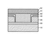
図2に示すように、基板10の上にカソード電極20が形成されており、そのカソード電極20の上にゲート絶縁層30が形成されている。前記ゲート絶縁層30には、後述するCNTエミッタが収容される貫通孔30aが形成されており、貫通孔30aの底部に電子放出のためのエミッタ50が設けられている。エミッタ50は、貫通孔30aの底に露出されたカソード電極20上に形成される。ここで、エミッタ50は、下部の抵抗物質層51とその上部の電子放出物質層52とが連続的に形成された積層構造を有する。一方、前記ゲート絶縁層30の上には、前記エミッタ50の電子放出物質層52から電子を抽出するゲートホール40aを有するゲート電極40が形成されている。
Hereinafter, embodiments of the present invention will be described in detail with reference to the accompanying drawings.
As shown in FIG. 2, a
前記電子放出物質層52は、所定の電界により電子放出が可能なCNTまたはナノサイズのパーティクルすなわちナノパーティクルを含む。また、さらに効果的な電流供給のために、前記電子放出物質層52には、高導電性の金属パーティクル、例えば銀が含まれることが望ましい。
The electron
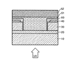
以上のような構造を有する本発明による電界放出素子によれば、図2に示されたように、電子放出物質層52の下部に抵抗物質層51が形成されているため、銀などの導電性粒子により高い導電性を有する電子放出物質層52に均一に分布しているCNTまたはナノパーティクルの放出点(端)まで電流が均一に供給され、エミッタの全面に亘って均一に電子(e-)が放出される。
According to the field emission device of the present invention having the above structure, as shown in FIG. 2, since the
以下、本発明による電界放出素子の製造方法の第1実施形態を説明する。
図3Aに示されたように、ソーダライムガラスからなる基板10にカソード電極20を形成する。カソード電極20はITO(Indium Tin Oxide)により形成され、これをフォトリソグラフィ法などによりパターニングする。
Hereinafter, a first embodiment of a method for manufacturing a field emission device according to the present invention will be described.
As shown in FIG. 3A, a
図3Bに示されたように、前記基板10の上にゲート絶縁層30を形成する。ゲート絶縁層30は、カソード電極20が部分的に露出される貫通孔30aを有する。このようなゲート絶縁層30は、スクリーン印刷法またはその他の公知の方法により形成することができる。
As shown in FIG. 3B, a
図3Cに示されたように、前記ゲート絶縁層30の上にゲート電極40を形成する。ゲート電極40は、前記貫通孔30aに対応するゲートホール40aを有し、薄膜形成工程または厚膜形成工程などにより金属物質の蒸着およびパターニングまたは金属ペーストのスクリーン印刷などにより形成される。
As shown in FIG. 3C, a
図3Cに示されたような基板構造物を得るための図3Aないし図3Cに示されたような工程は、公知のものであり、この基板構造物は、前述の方法以外の方法によっても形成することができる。以下の過程は前記過程に続くものであり、本発明を特徴づける次の段階を含む。図4Aないし図4Fは、理解を助けるために、一つのエミッタおよびゲートホールに対応する構造を抜粋して図示する。 The steps shown in FIGS. 3A to 3C for obtaining the substrate structure as shown in FIG. 3C are known, and this substrate structure may be formed by a method other than the method described above. can do. The following process follows the above process and includes the following steps that characterize the invention. FIGS. 4A to 4F illustrate a structure corresponding to one emitter and a gate hole for ease of understanding.
図4Aに示されたように、前記貫通孔30aの底を除いて、ゲート電極40の表面および貫通孔30aの内壁に、リフトオフ法のための犠牲層60がフォトレジストで形成される。
As shown in FIG. 4A, a
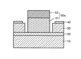
図4Bに示されたように、ペーストを用いるスクリーン印刷またはゾル−ゲルもしくはスラリを用いるスピンコーティングなどのコーティング工程によって、前記犠牲層60の上にフォトレジストを含む抵抗物質層51が形成される。抵抗物質層51は、コーティング工程の間、前記貫通孔30aの内部を覆っている。
As shown in FIG. 4B, a
図4Cに示されたように、前記抵抗物質層51の上に、フォトレジストおよび電子放出が可能な物質、例えばCNTまたはナノパーティクルを含むペースト状態の電子放出物質層52を形成する。このペーストには、効果的な電流供給のための導電性粒子、例えば銀が含まれる。
Referring to FIG. 4C, a paste and an electron
図4Dに示されたように、加熱または紫外線(UV)により抵抗物質層51と電子放出物質層52とを硬化させる。
As shown in FIG. 4D, the
図4Eに示されたように、エッチング液を利用して前記犠牲層60を除去するリフトオフを実施し、前記貫通孔30aの底部中央にだけ抵抗物質層51および電子放出物質層52による初期形態のエミッタ50を形成する。
As shown in FIG. 4E, lift-off is performed to remove the
図4Fに示されたように、所定温度下で焼成して前記エミッタ50を完全に硬化させつつ収縮させることにより、電子放出物質層52をゲートホール40aの下部に下げることにより目的とする電界放出素子が得られる。
As shown in FIG. 4F, by firing at a predetermined temperature, the
前記の通り、本発明の特徴は、エミッタが、電流を制限する抵抗物質層と電子放出が起きる電子放出物質層とによる積層構造を有することにある。このような構造によって、すなわち、本発明による電界放出素子は、導電性物質と抵抗性物質の特性を利用するエミッタを備える。このような構造によれば、電子放出物質層の放出点までの電流の供給がいくつかの限定された経路で供給される従来の電界放出素子とは異なり、抵抗物質層を電子放出物質層の下部の電流経路上に設けることにより、抵抗物質層を通過した電子によって導電性の高い電子放出物質層に電流が均一に供給されて多数の放出点まで電流が円滑に供給される。 As described above, the feature of the present invention resides in that the emitter has a laminated structure including a resistive material layer for limiting a current and an electron emitting material layer for emitting electrons. Due to such a structure, that is, the field emission device according to the present invention includes an emitter using characteristics of a conductive material and a resistive material. According to such a structure, unlike the conventional field emission device in which the current supply to the emission point of the electron emission material layer is supplied through some limited paths, the resistance material layer is replaced with the electron emission material layer. By providing it on the lower current path, the electrons that have passed through the resistive material layer uniformly supply the current to the highly conductive electron emitting material layer, and the current is smoothly supplied to many emission points.
一方、前記電子放出物質層52とその下部の抵抗物質層51とをリフトオフしてエミッタ50を形成した後にも電子放出物質の一部がゲートホール40aの周囲に残留する可能性がある。このような不必要な電子放出物質は、エミッタ50とゲート電極40とを電気的にショートさせる可能性があるため除去せねばならない。
On the other hand, even after the
このような電子放出物質の残留は、使われる抵抗物質層と犠牲層間の化学的結合に起因する。すなわち、電界放出素子の製造時に生じる犠牲層と電子放出物質間の接触によって、それら両者間の反応が誘発される可能性が非常に高い。これは、2物質がいずれも感光性物質を含む樹脂からなるためであると見られる。犠牲層の材料として用いられる樹脂はノボラック系の感光性樹脂である。この成分の樹脂に対して強い溶解性を有する溶媒、例えばテキサノール(商品名、2,2,4-Trimethyl-1,3-pentandiolmonoisobutyrat)が電子放出物質に添加されている場合、犠牲層に対する溶媒の攻撃が避けられない。すなわち、2層の接触によって、溶解性の強いテキサノールが、犠牲層のノボラックマトリックスを溶かし、溶解されたノボラックマトリックス成分が電子放出物質に存在するアクリリックマトリックスと混合されて、2マトリックス間の強い結合が誘導される。このような状態になった場合には、現像液またはリフトオフ用溶媒を利用したエミッタのパターニングが不可能である。従って、本発明の第2実施形態による電界放出素子の製造方法においては、基本的にリフトオフ時に、犠牲層として使われる物質と、エミッタ形成のための電子放出物質との間の工程中での接触を防止するための隔離層として前述した抵抗物質層を利用し、この抵抗物質層に後述する非反応性物質が含まれる。 Such a residue of the electron emitting material is caused by a chemical bond between the used resistive material layer and the sacrificial layer. That is, there is a very high possibility that the contact between the sacrificial layer and the electron-emitting substance generated during the manufacture of the field emission device will induce a reaction between them. This is considered to be because the two substances are both made of a resin containing a photosensitive substance. The resin used as the material of the sacrificial layer is a novolak-based photosensitive resin. When a solvent having strong solubility in the resin of this component, for example, Texanol (trade name, 2,2,4-Trimethyl-1,3-pentandiolmonoisobutyrat) is added to the electron-emitting substance, Attacks are inevitable. That is, due to the contact between the two layers, the highly soluble texanol dissolves the novolak matrix of the sacrificial layer, and the dissolved novolak matrix component is mixed with the acrylic matrix present in the electron-emitting substance, and a strong bond between the two matrices is formed. Be guided. In such a state, it is impossible to pattern the emitter using a developer or a lift-off solvent. Accordingly, in the method of manufacturing the field emission device according to the second embodiment of the present invention, the contact between the material used as the sacrificial layer and the electron emission material for forming the emitter during the lift-off process is basically made. The above-described resistive material layer is used as an isolation layer for preventing the occurrence of a non-reactive material, which will be described later.
以下の実施形態では、このような電子放出物質の残留を効果的に防止するための他の方法が説明される。本発明の第2実施形態でも、やはり前述した図3Aないし図3Cに示されたような工程を通じて基板構造物をまず準備した後、次のような後続工程を行う。 In the following embodiments, other methods for effectively preventing such a residual electron-emitting substance will be described. In the second embodiment of the present invention, a substrate structure is first prepared through the processes shown in FIGS. 3A to 3C, and then the following processes are performed.
図5Aに示されたように、前記貫通孔30aの底を除いて、ゲート電極40の表面および貫通孔30aの内壁に、リフトオフのための犠牲層60が、フォトレジストによって形成される。犠牲層60は、ペーストを利用するスクリーン印刷、ゾル−ゲルまたはスラリ溶液を利用するスピンコーティングにより形成してソフトベークされる。
As shown in FIG. 5A, a
図5Bに示されたように、前記犠牲層60の上に、犠牲層60およびその犠牲層60の上に形成される電子放出物質層のうち少なくとも一つと反応しない抵抗物質層51aが形成される。抵抗物質層51aは、犠牲層60と同様に、ペーストを利用するスクリーン印刷、ゾル−ゲルまたはスラリ溶液を利用するスピンコーティングにより形成した後でソフトベークされる。ここで、前記抵抗物質層51aを形成するための物質は、前記犠牲層60と反応性がないか、工程上で妨害にならないほどのきわめて弱い反応性を有することが必要である。このような非反応性は、前記抵抗物質層51aの上に形成される電子放出物質に対しても保持されることが望ましい。そして、前記抵抗物質層51aには、前述のようにエミッタの下部に抵抗物質層を形成するために抵抗性物質が含まれていることが好ましく、また感光性フォトレジストも含まれうる。ここで用いることができる抵抗性物質としては、SiO2、MgO、a−Si、p−Siがあり、これらのうち少なくとも一つを用いることができる。
As shown in FIG. 5B, a
図5Cに示されたように、フォトレジストおよび電子放出が可能な物質、例えばCNTまたはナノパーティクルを含む電子放出物質層52が、抵抗物質層51aの上に形成される。このペーストには、効果的な電流供給のための導電性粒子、例えば銀が含まれることが望ましい。このような電子放出物質層52は、ペーストを利用するスクリーン印刷、ゾル−ゲルまたはスラリ溶液を利用するスピンコーティングなどにより形成することができる。
As shown in FIG. 5C, an electron
図5Dに示されたように、加熱またはUVによって、犠牲層60、抵抗物質層51aおよび電子放出物質層52を硬化させる。
As shown in FIG. 5D, the
図5Eに示されたように、エッチング液を用いて前記犠牲層60を除去するリフトオフを実施し、前記貫通孔30aの底部中央にだけ抵抗物質層51aおよび電子放出物質層52で構成される初期形態のエミッタ50aが形成される。
As shown in FIG. 5E, lift-off is performed to remove the
図5Fに示されたように、所定温度で焼成して前記エミッタ50aを完全に硬化させつつ収縮させることにより、エミッタ50aの上端部をゲートホール40aの下部まで下げる。焼成によって基板構造物の上に形成された積層物から熱分解性成分が全て除去される。
As shown in FIG. 5F, the upper end of the
前記のとおり、本発明の製造方法の第2実施形態の特徴は、犠牲層と電子放出物質層の間に非反応性の抵抗物質層を介在させることにより、フォトレジストを含む犠牲層と電子放出物質層との間の反応を防止し、従って、それらの間の強い結合を防止することにより、エミッタ形成のためのリフトオフが効果的に行うことができるということである。また、抵抗物質層によって、導電性の高い電子放出物質層に電流が均一に供給され、エミッタの全面に均一な電子放出が可能になる。 As described above, the feature of the second embodiment of the manufacturing method of the present invention is that the non-reactive resistive material layer is interposed between the sacrificial layer and the electron-emitting material layer, so that the sacrificial layer including the photoresist and the electron-emitting By preventing the reaction with the material layers and thus the strong coupling between them, the lift-off for the emitter formation can be effected effectively. In addition, the resistance material layer uniformly supplies a current to the highly conductive electron emission material layer, thereby enabling uniform emission of electrons over the entire surface of the emitter.
前記第2実施形態において、抵抗性物質は、犠牲層および電子放出物質層と反応しないが、次の第3実施形態および第4実施形態においては、相互に反応してはならない犠牲層と電子放出物質層の間に形成される積層物に別途の隔離層を挿入することにより、リフトオフ後においても、不要な電子放出物質の残留を防止できる。 In the second embodiment, the resistive material does not react with the sacrifice layer and the electron emission material layer. However, in the following third and fourth embodiments, the sacrifice layer and the electron emission layer which must not react with each other. By inserting a separate isolation layer into the stack formed between the material layers, unnecessary electron emission materials can be prevented from remaining even after lift-off.
以下、本発明の第3実施形態による電界放出素子の製造方法について段階的に説明する。本実施形態においても、前述した図3Aないし図3Cに示された工程を通じて基板構造物をまず準備した後、次のような後続の工程を行う。 Hereinafter, the method of manufacturing the field emission device according to the third embodiment of the present invention will be described step by step. In the present embodiment, a substrate structure is first prepared through the processes shown in FIGS. 3A to 3C, and then the following processes are performed.
図6Aに示されたように、前記貫通孔30aの底を除いて、ゲート電極40の表面および貫通孔30aの内壁に、リフトオフのための犠牲層60を形成する。犠牲層60は、ペーストを利用するスクリーン印刷、ゾル−ゲルまたはスラリ溶液を利用するスピンコーティングにより形成した後にソフトベークされる。
As shown in FIG. 6A, a
図6Bに示されたように、前記犠牲層60の上に、犠牲層60およびその犠牲層60の上に形成される抵抗物質層51のうち少なくとも一つと反応しない隔離層80が形成される。この隔離層80は、ペーストを利用するスクリーン印刷、ゾル−ゲルまたはスラリ溶液を利用するスピンコーティングにより形成した後、ソフトベークされる。
As shown in FIG. 6B, on the
図6Cに示されたように、前記隔離層80の上に、抵抗物質層51が形成される。抵抗物質層51もやはりペーストを利用したスクリーン印刷、ゾル−ゲルまたはスラリ溶液を利用するスピンコーティングにより形成した後、ソフトベークされる。ここで、前記抵抗物質層51は、感光性樹脂を含んでいてもよい。ここで、抵抗性物質として、SiO2、MgO、a−Siおよびp−Siのうち少なくとも一つを用いることができる。
As shown in FIG. 6C, a
図6Dに示されたように、感光性樹脂および電子放出の可能な物質、例えばCNTまたはナノパーティクルを含む電子放出物質層52が、抵抗物質層51の上に形成される。この電子放出物質層52は、効果的な電流供給のための導電性粒子、例えば銀が含まれることが望ましい。このような電子放出物質層52は、ペーストを利用するスクリーン印刷、ゾル−ゲルまたはスラリ溶液を利用するスピンコーティング等により形成することができる。
As shown in FIG. 6D, an electron
図6Eに示されたように、加熱またはUVによって、犠牲層60、隔離層80、抵抗物質層51および電子放出物質層52を硬化させる。
As shown in FIG. 6E, the
図6Fに示されたように、エッチング液を用いて前記犠牲層60を除去するリフトオフを実施し、前記貫通孔30aの底部中央に、隔離層80と、この隔離層80の上部に形成される抵抗物質層51と、電子放出物質層52とによる初期形態のエミッタ50aが形成される。
As shown in FIG. 6F, lift-off is performed to remove the
図6Gに示されたように、所定温度で焼成して前記エミッタ50aを完全に硬化させつつ収縮させることにより、エミッタ50aの上端部をゲートホール40aの下部にまで下げる。焼成によって、基板構造物の上に形成された積層物から熱分解性成分、特に隔離層80が除去される。
As shown in FIG. 6G, the upper end of the
以下、本発明の電界放出素子の製造方法に係る第4実施形態を段階的に説明する。本実施形態でもやはり前述した図3Aないし図3Cに示されたような工程を通じて基板構造物をまず準備した後、次のような後続の工程を行う。 Hereinafter, a fourth embodiment of the method for manufacturing a field emission device according to the present invention will be described step by step. In this embodiment, the substrate structure is first prepared through the processes shown in FIGS. 3A to 3C, and then the following processes are performed.
図7Aに示されたように、前記貫通孔30aの底部を除いて、ゲート電極40の表面および貫通孔30aの内壁に、リフトオフのための犠牲層60がフォトレジストで形成される。犠牲層60は、ペーストを利用するスクリーン印刷、ゾル−ゲルまたはスラリ溶液を利用するスピンコーティングなどにより形成した後、ソフトベークされる。
As shown in FIG. 7A, a
図7Bに示されたように、前記犠牲層60の上に抵抗物質層51を形成する。抵抗物質層51もやはりペーストを利用するスクリーン印刷、ゾル−ゲルまたはスラリ溶液を利用するスピンコーティングなどにより形成した後、ソフトベークされる。ここで、前記抵抗物質層51は、感光性樹脂を含んでいてもよい。ここで、抵抗性物質としては、SiO2、MgO、a−Si、およびp−Siのうち少なくとも一つを用いることができる。
7B, a
図7Cに示されたように、前記犠牲層60の上に、犠牲層60およびその犠牲層60の上に形成される抵抗物質層51のうち少なくとも一つと反応しない隔離層80aが形成される。この隔離層80aは、ペーストを利用するスクリーン印刷、ゾル−ゲルまたはスラリ溶液を利用するスピンコーティングなどにより形成した後、ソフトベークされる。
As shown in FIG. 7C, an
図7Dに示されたように、感光性樹脂および電子放出の可能な物質、例えばCNTまたはナノパーティクルを含む電子放出物質層52が、前記隔離層80aの上に形成される。この電子放出物質層52には、効果的な電流供給のための導電性粒子、例えば銀が含まれることが望ましい。このような電子放出物質層52は、ペーストを利用するスクリーン印刷、ゾル−ゲルまたはスラリ溶液を利用するスピンコーティングなどにより形成できる。
As shown in FIG. 7D, an electron
図7Eに示されたように、加熱またはUVによって、犠牲層60、隔離層80a、抵抗物質層51aおよび電子放出物質層52を硬化させる。
As shown in FIG. 7E, the
図7Fに示されたように、エッチング液を利用して前記犠牲層60を除去するリフトオフを実施し、前記貫通孔30aの底部中央に、隔離層80と、この隔離層80の上部に形成される抵抗物質層51と、電子放出物質層52とによって初期形態のエミッタ50aが形成される。
As shown in FIG. 7F, lift-off is performed to remove the
図7Gに示されたように、所定温度で焼成して前記エミッタ50aを完全に硬化させつつ収縮させることにより、エミッタ50aの上端部をゲートホール40aの下部にまで下げる。焼成によって基板構造物の上に形成された積層物から熱分解性成分、特に隔離層80aが除去される。
As shown in FIG. 7G, the upper end of the
本発明は、図面に示された実施形態を参考として説明されたが、これは例示に過ぎず、当技術分野の当業者ならば、これらの実施形態から多様な変形および均等な他の実施形態が想到可能であるという点が理解できるであろう。従って、本発明の真の技術的保護範囲は、特許請求の範囲に限って決められるべきである。 Although the present invention has been described with reference to the embodiments illustrated in the drawings, this is by way of example only, and those skilled in the art will appreciate that various modifications and equivalents of these embodiments may occur. It can be understood that is possible. Therefore, the true technical scope of the present invention should be determined only by the appended claims.
本発明は、電子放出源として平板型ディスプレイ装置に適用され、さらに電子ソースを要求するいかなる装置にも適用可能である。 INDUSTRIAL APPLICABILITY The present invention is applied to a flat panel display device as an electron emission source, and is applicable to any device requiring an electron source.
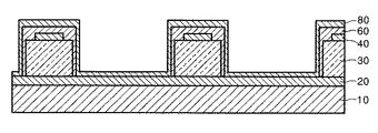
10 基板
20 カソード電極
30 ゲート絶縁層
30a 貫通孔
40 ゲート電極
40a ゲートホール
50a エミッタ
51 抵抗物質層
52 電子放出物質層
e- 電子
DESCRIPTION OF
Claims (43)
前記基板上に形成されるカソード電極と、
前記カソード電極上に形成され、前記カソード電極の一部に対応する貫通孔を有するゲート絶縁層と、
前記貫通孔に対応するゲートホールを有し、前記ゲート絶縁層上に形成されるゲート電極と、
前記貫通孔の下部に露出された前記ゲート電極上に形成される電子エミッタとを備え、
前記電子エミッタは、抵抗物質層と、前記抵抗物質層上に形成される微細電子放出源を含有する電子放出物質層とによる積層構造を有することを特徴とする電界放出素子。 Board and
A cathode electrode formed on the substrate;
A gate insulating layer formed on the cathode electrode and having a through hole corresponding to a part of the cathode electrode;
Having a gate hole corresponding to the through hole, a gate electrode formed on the gate insulating layer,
An electron emitter formed on the gate electrode exposed below the through hole,
The field emission device according to claim 1, wherein the electron emitter has a laminated structure including a resistance material layer and an electron emission material layer containing a fine electron emission source formed on the resistance material layer.
b)前記貫通孔の下部に露出されたカソード電極を除いて、基板構造物の表面および前記貫通孔の内壁に犠牲層を形成する段階と、
c)前記基板構造物の表面に抵抗物質を所定厚さに塗布して前記貫通孔を前記抵抗物質を埋め込み、電子放出物質層をその上部に積層形成する段階と、
d)前記ゲート電極の表面と前記貫通孔の内壁とに形成された前記犠牲層を除去するためエッチング液によるリフトオフ法によって、前記貫通孔の内側領域に、前記抵抗物質層と、その抵抗物質層の上部の電子放出物質層とで構成されるエミッタを形成する段階と、
e)前記エミッタを焼成する段階とを含むことを特徴とする電界放出素子の製造方法。 a) A cathode electrode is formed on a substrate, and a gate insulating layer having a through hole partially exposing the cathode electrode and a gate electrode having a gate hole corresponding to the through hole are sequentially laminated on the cathode electrode. Providing a substrate structure that has been
b) forming a sacrificial layer on the surface of the substrate structure and on the inner wall of the through hole except for the cathode electrode exposed below the through hole;
c) applying a resistive material to the surface of the substrate structure to a predetermined thickness, filling the through-hole with the resistive material, and forming an electron emission material layer on the upper surface thereof;
d) removing the sacrificial layer formed on the surface of the gate electrode and the inner wall of the through hole by a lift-off method using an etchant in the inner region of the through hole; Forming an emitter consisting of an electron emitting material layer on top of
e) firing the emitter.
b)前記貫通孔の下部に露出されたカソード電極を除いて、基板構造物の表面および前記貫通孔の内壁の全体に犠牲層を形成する段階と、
c)前記犠牲層の上に、前記ゲート電極の上にエミッタを形成するための電子放出物質層と前記犠牲層との接触を防止して前記犠牲層と前記電子放出物質層のうち少なくとも一つと反応しない抵抗物質層を形成する段階と、
d)前記犠牲層が形成された基板構造物の表面に電子放出物質を所定厚さに塗布し、前記貫通孔に前記電子放出物質を埋め込み、電子放出物質層を形成する段階と、
e)ゲート電極の表面と前記貫通孔の内壁とに形成された前記犠牲層を除去するためにエッチング液によるリフトオフを実施し、前記犠牲層の上に形成された抵抗物質層および電子放出物質層を除去して前記貫通孔の内側領域に前記抵抗物質層および電子放出物質層によるエミッタを形成する段階と、
f)前記エミッタを焼成する段階とを含むことを特徴とする電界放出素子の製造方法。 a) A cathode electrode is formed on a substrate, and a gate insulating layer having a through hole partially exposing the cathode electrode and a gate electrode having a gate hole corresponding to the through hole are sequentially laminated on the cathode electrode. Providing a substrate structure,
b) forming a sacrificial layer on the surface of the substrate structure and on the entire inner wall of the through hole except for the cathode electrode exposed below the through hole;
c) on the sacrificial layer, preventing contact between the electron-emitting material layer for forming an emitter on the gate electrode and the sacrificial layer to form at least one of the sacrificial layer and the electron-emitting material layer; Forming a non-reactive resistance material layer;
d) applying an electron emitting material to a predetermined thickness on a surface of the substrate structure on which the sacrificial layer is formed, filling the through hole with the electron emitting material, and forming an electron emitting material layer;
e) performing a lift-off with an etchant to remove the sacrificial layer formed on the surface of the gate electrode and the inner wall of the through hole, and forming a resistive material layer and an electron emitting material layer formed on the sacrificial layer Forming an emitter of the resistive material layer and the electron-emitting material layer in the inner region of the through-hole,
f) firing the emitter.
b)前記貫通孔の下部に露出されたカソード電極を除いて、基板構造物の表面および前記貫通孔の内壁の全体に犠牲層を形成する段階と、
c)前記犠牲層とその上に形成される抵抗物質層とを相互隔離してそれらのうち少なくともいずれか一つと非反応性を有する隔離層を形成する段階と、
d)前記隔離層の上に電気的抵抗性を有する抵抗物質層を形成する段階と、
e)前記隔離層が形成された基板構造物の表面に電子放出物質を所定厚さに塗布し、前記貫通孔に前記電子放出物質を埋め込み、電子放出物質層を形成する段階と、
f)前記ゲート電極の表面と前記貫通孔の内壁とに形成された前記犠牲層を除去するためにエッチング液によるリフトオフを実施し、前記犠牲層の上に形成された隔離層、抵抗物質層および電子放出物質層を除去して前記貫通孔の内側領域に前記抵抗物質層および前記電子放出物質層によるエミッタを形成する段階と、
g)前記エミッタを焼成する段階とを含むことを特徴とする電界放出素子の製造方法。 a) A cathode electrode is formed on a substrate, and a gate insulating layer having a through hole partially exposing the cathode electrode and a gate electrode having a gate hole corresponding to the through hole are sequentially laminated on the cathode electrode. Providing a substrate structure,
b) forming a sacrificial layer on the surface of the substrate structure and on the entire inner wall of the through hole except for the cathode electrode exposed below the through hole;
c) isolating the sacrificial layer and the resistive material layer formed thereon from each other to form an isolation layer that is non-reactive with at least one of them.
d) forming a resistive material layer having electrical resistance on the isolation layer;
e) applying an electron emitting material to a predetermined thickness on the surface of the substrate structure on which the isolation layer is formed, filling the through hole with the electron emitting material, and forming an electron emitting material layer;
f) performing lift-off with an etchant to remove the sacrificial layer formed on the surface of the gate electrode and the inner wall of the through hole, and forming an isolation layer, a resistive material layer, and a resistive material layer formed on the sacrificial layer; Removing the electron emitting material layer to form an emitter using the resistive material layer and the electron emitting material layer in an area inside the through hole;
g) firing the emitter.
b)前記貫通孔の下部に露出されたカソード電極を除いて、基板構造物の表面および前記貫通孔の内壁の全体に犠牲層を形成する段階と、
c)前記犠牲層の上に電気的抵抗性を有する抵抗物質層を形成する段階と、
d)前記抵抗物質層とその上に形成される電子放出物質層とを相互隔離し、それらのうち少なくともいずれか一つと非反応性を有する隔離層を形成する段階と、
e)前記隔離層が形成された基板構造物の表面に電子放出物質を所定厚さに塗布し、前記貫通孔に前記電子放出物質を埋め込み、電子放出物質層を形成する段階と、
f)前記ゲート電極の表面と前記貫通孔の内壁とに形成された前記犠牲層を除去するためにエッチング液によるリフトオフを実施し、前記犠牲層の上に形成された抵抗物質層、前記隔離層および電子放出物質を除去して前記貫通孔の内側領域に前記抵抗物質層および電子放出物質層を含むエミッタを形成する段階と、
g)前記エミッタを焼成する段階とを含むことを特徴とする電界放出素子の製造方法。 a) A cathode electrode is formed on a substrate, and a gate insulating layer having a through hole partially exposing the cathode electrode and a gate electrode having a gate hole corresponding to the through hole are sequentially laminated on the cathode electrode. Providing a substrate structure,
b) forming a sacrificial layer on the surface of the substrate structure and on the entire inner wall of the through hole except for the cathode electrode exposed below the through hole;
c) forming a resistive material layer having electrical resistance on the sacrificial layer;
d) isolating the resistive material layer and the electron emitting material layer formed thereon from each other, and forming an isolating layer that is non-reactive with at least one of them.
e) applying an electron emitting material to a predetermined thickness on the surface of the substrate structure on which the isolation layer is formed, filling the through hole with the electron emitting material, and forming an electron emitting material layer;
f) performing a lift-off using an etchant to remove the sacrificial layer formed on the surface of the gate electrode and the inner wall of the through hole, and forming a resistive material layer formed on the sacrificial layer and the isolation layer; Removing the electron emitting material and forming an emitter including the resistive material layer and the electron emitting material layer in an inner region of the through hole;
g) firing the emitter.
Applications Claiming Priority (2)
| Application Number | Priority Date | Filing Date | Title |
|---|---|---|---|
| KR20020081865 | 2002-12-20 | ||
| KR10-2003-0015360A KR100519762B1 (en) | 2002-12-20 | 2003-03-12 | Manufacturing methode of field emission device |
Publications (1)
| Publication Number | Publication Date |
|---|---|
| JP2004207239A true JP2004207239A (en) | 2004-07-22 |
Family
ID=32658663
Family Applications (1)
| Application Number | Title | Priority Date | Filing Date |
|---|---|---|---|
| JP2003423929A Pending JP2004207239A (en) | 2002-12-20 | 2003-12-22 | Field emission device and its manufacturing method |
Country Status (2)
| Country | Link |
|---|---|
| US (1) | US7044822B2 (en) |
| JP (1) | JP2004207239A (en) |
Cited By (1)
| Publication number | Priority date | Publication date | Assignee | Title |
|---|---|---|---|---|
| JP2006040863A (en) * | 2004-07-26 | 2006-02-09 | Samsung Sdi Co Ltd | Field emission display equipped with carbon nanotube emitter, and its manufacturing method |
Families Citing this family (6)
| Publication number | Priority date | Publication date | Assignee | Title |
|---|---|---|---|---|
| JP4252546B2 (en) * | 2004-03-24 | 2009-04-08 | 三菱電機株式会社 | Method for manufacturing field emission display device |
| US7834530B2 (en) * | 2004-05-27 | 2010-11-16 | California Institute Of Technology | Carbon nanotube high-current-density field emitters |
| KR20050115057A (en) * | 2004-06-03 | 2005-12-07 | 삼성에스디아이 주식회사 | A long life-time field emitter for a field emission device and a method for fabricating the same |
| JP5102968B2 (en) * | 2006-04-14 | 2012-12-19 | 株式会社日立ハイテクノロジーズ | Conductive needle and method of manufacturing the same |
| CN101777473B (en) * | 2010-03-10 | 2012-01-04 | 彩虹集团公司 | Dense material thin-layer sizing agent of carbon nanotube field emission device and method for manufacturing structure |
| CN102509679B (en) * | 2011-11-08 | 2014-10-01 | 福州大学 | Electronic emission source of nanometer material-medium-nanometer material structure |
Citations (12)
| Publication number | Priority date | Publication date | Assignee | Title |
|---|---|---|---|---|
| JPH08321253A (en) * | 1995-05-24 | 1996-12-03 | Fujitsu Ltd | Electric field emitting cathode and its manufacture |
| JPH09161659A (en) * | 1995-12-13 | 1997-06-20 | Dainippon Printing Co Ltd | Electron emitting element and manufacture thereof |
| JPH1031954A (en) * | 1996-07-12 | 1998-02-03 | Futaba Corp | Field emitting element and its manufacture |
| JPH1092295A (en) * | 1996-09-12 | 1998-04-10 | Nec Corp | Field emission type cold cathode |
| JP2000149816A (en) * | 1998-09-08 | 2000-05-30 | Matsushita Electric Ind Co Ltd | Resistor for cathode ray tube, its manufacture, cathode ray tube and fed |
| JP2000268701A (en) * | 1999-03-15 | 2000-09-29 | Toshiba Corp | Electron emitting element, its manufacture, display element and its manufacture |
| JP2001035361A (en) * | 1999-07-16 | 2001-02-09 | Futaba Corp | Manufacture of electron emitting source, the electron emitting source and fluorescent type display |
| JP2002203469A (en) * | 2000-12-27 | 2002-07-19 | Toshiba Corp | Cold cathode electronic device |
| JP2002208345A (en) * | 2001-01-09 | 2002-07-26 | Sony Corp | Manufacturing method of cold cathode field electron emission element and manufacturing method of cold cathode field electron emission display device |
| JP2002245928A (en) * | 2001-01-05 | 2002-08-30 | Samsung Sdi Co Ltd | Method of manufacturing field discharge array of triode carbon nanotube |
| JP2002270087A (en) * | 2001-03-14 | 2002-09-20 | Sony Corp | Method of manufacturing cold cathode field electron emission element and method of manufacturing cold cathode field electron emission display device |
| JP2002341525A (en) * | 2001-05-14 | 2002-11-27 | Fuji Photo Film Co Ltd | Positive photoresist transfer material and method for working surface of substrate using the same |
Family Cites Families (18)
| Publication number | Priority date | Publication date | Assignee | Title |
|---|---|---|---|---|
| US4659136A (en) * | 1984-04-13 | 1987-04-21 | Martin John W | Collapsible enclosure apparatus |
| US5018777A (en) * | 1990-03-27 | 1991-05-28 | Swenson Gleo S | Hinge and connection assembly for removable truck topper |
| JP3223650B2 (en) | 1993-06-25 | 2001-10-29 | 双葉電子工業株式会社 | Field emission cathode |
| KR100205051B1 (en) * | 1995-12-22 | 1999-06-15 | 정선종 | Manufacturing method of field emission display device |
| US6042173A (en) * | 1997-02-06 | 2000-03-28 | Covercraft Industries, Inc. | Hard shell tonneau cover |
| US6168491B1 (en) * | 1998-03-23 | 2001-01-02 | The United States Of America As Represented By The Secretary Of The Navy | Method of forming field emitter cell and array with vertical thin-film-edge emitter |
| US6084245A (en) * | 1998-03-23 | 2000-07-04 | The United States Of America As Represented By The Secretary Of The Navy | Field emitter cell and array with vertical thin-film-edge emitter |
| JP2000011859A (en) * | 1998-06-22 | 2000-01-14 | Yamaha Corp | Manufacture of field emission type element |
| US6297587B1 (en) * | 1998-07-23 | 2001-10-02 | Sony Corporation | Color cathode field emission device, cold cathode field emission display, and process for the production thereof |
| US6465941B1 (en) * | 1998-12-07 | 2002-10-15 | Sony Corporation | Cold cathode field emission device and display |
| KR20000074609A (en) | 1999-05-24 | 2000-12-15 | 김순택 | Carbon nano tube field emission array and fabricating method thereof |
| KR20010046796A (en) | 1999-11-15 | 2001-06-15 | 김덕중 | Field emission display device and manufacturing method thereof |
| KR100480773B1 (en) | 2000-01-07 | 2005-04-06 | 삼성에스디아이 주식회사 | Method for fabricating triode-structure carbon nanotube field emitter array |
| JP2001234163A (en) * | 2000-02-25 | 2001-08-28 | Sony Corp | Luminous crystalline particle, luminous crystalline particle composition, display panel and flat-surface display device |
| KR20010035361A (en) | 2001-02-07 | 2001-05-07 | 박성조 | Clamping device for clamping a handphone holding neckrace to clothes |
| US6440763B1 (en) * | 2001-03-22 | 2002-08-27 | The United States Of America As Represented By The Secretary Of The Navy | Methods for manufacture of self-aligned integrally gated nanofilament field emitter cell and array |
| GB2383187B (en) * | 2001-09-13 | 2005-06-22 | Microsaic Systems Ltd | Electrode structures |
| KR100513727B1 (en) * | 2003-02-12 | 2005-09-08 | 삼성에스디아이 주식회사 | Manufacturing method of a field emission device |
-
2003
- 2003-12-16 US US10/735,741 patent/US7044822B2/en not_active Expired - Fee Related
- 2003-12-22 JP JP2003423929A patent/JP2004207239A/en active Pending
Patent Citations (12)
| Publication number | Priority date | Publication date | Assignee | Title |
|---|---|---|---|---|
| JPH08321253A (en) * | 1995-05-24 | 1996-12-03 | Fujitsu Ltd | Electric field emitting cathode and its manufacture |
| JPH09161659A (en) * | 1995-12-13 | 1997-06-20 | Dainippon Printing Co Ltd | Electron emitting element and manufacture thereof |
| JPH1031954A (en) * | 1996-07-12 | 1998-02-03 | Futaba Corp | Field emitting element and its manufacture |
| JPH1092295A (en) * | 1996-09-12 | 1998-04-10 | Nec Corp | Field emission type cold cathode |
| JP2000149816A (en) * | 1998-09-08 | 2000-05-30 | Matsushita Electric Ind Co Ltd | Resistor for cathode ray tube, its manufacture, cathode ray tube and fed |
| JP2000268701A (en) * | 1999-03-15 | 2000-09-29 | Toshiba Corp | Electron emitting element, its manufacture, display element and its manufacture |
| JP2001035361A (en) * | 1999-07-16 | 2001-02-09 | Futaba Corp | Manufacture of electron emitting source, the electron emitting source and fluorescent type display |
| JP2002203469A (en) * | 2000-12-27 | 2002-07-19 | Toshiba Corp | Cold cathode electronic device |
| JP2002245928A (en) * | 2001-01-05 | 2002-08-30 | Samsung Sdi Co Ltd | Method of manufacturing field discharge array of triode carbon nanotube |
| JP2002208345A (en) * | 2001-01-09 | 2002-07-26 | Sony Corp | Manufacturing method of cold cathode field electron emission element and manufacturing method of cold cathode field electron emission display device |
| JP2002270087A (en) * | 2001-03-14 | 2002-09-20 | Sony Corp | Method of manufacturing cold cathode field electron emission element and method of manufacturing cold cathode field electron emission display device |
| JP2002341525A (en) * | 2001-05-14 | 2002-11-27 | Fuji Photo Film Co Ltd | Positive photoresist transfer material and method for working surface of substrate using the same |
Cited By (1)
| Publication number | Priority date | Publication date | Assignee | Title |
|---|---|---|---|---|
| JP2006040863A (en) * | 2004-07-26 | 2006-02-09 | Samsung Sdi Co Ltd | Field emission display equipped with carbon nanotube emitter, and its manufacturing method |
Also Published As
| Publication number | Publication date |
|---|---|
| US20040124756A1 (en) | 2004-07-01 |
| US7044822B2 (en) | 2006-05-16 |
Similar Documents
| Publication | Publication Date | Title |
|---|---|---|
| US6812480B2 (en) | Triode structure field emission display device using carbon nanotubes and method of fabricating the same | |
| US20040043219A1 (en) | Pattern forming method for carbon nanotube, and field emission cold cathode and method of manufacturing the cold cathode | |
| JP4865434B2 (en) | Electron emitter for thermionic emission, electron-emitting device including the same, and flat panel display device including the same | |
| KR20030078024A (en) | Cold cathode field emission device and process for the production thereof, and cold cathode field emission display and process for the production thereof | |
| US6803708B2 (en) | Barrier metal layer for a carbon nanotube flat panel display | |
| US20040036401A1 (en) | Field electron emission apparatus and method for manufacturing the same | |
| JP2004207239A (en) | Field emission device and its manufacturing method | |
| JP2007103346A (en) | Electron emitting element, electron emission display device, and its manufacturing method | |
| JP4469188B2 (en) | Manufacturing method of field emission device | |
| US7056753B2 (en) | Field emission display with double gate structure and method of manufacturing therefor | |
| KR100519762B1 (en) | Manufacturing methode of field emission device | |
| JP2005116500A (en) | Field emission display device and its manufacturing method | |
| JP2007026711A (en) | Micro electron source device and its manufacturing method, planar light-emitting device, and planar display device | |
| KR100724369B1 (en) | Field emission device with ultraviolet protection layer and manufacturing method thereof | |
| KR20060029079A (en) | Method of fabricating electron emission device | |
| TWI385697B (en) | Method for fabricating cathode planes for field emission | |
| JP2005044818A (en) | Electron emission element, electron source and image forming device | |
| KR20070056614A (en) | Method for manufacturing electron emission device | |
| KR20090054675A (en) | Electron emission device, method of manufacturing the same, and electron emission display including the same | |
| JP2006012700A (en) | Manufacturing method of electron emitting element and display device | |
| KR20070046609A (en) | Structure of electron emission source array, electron emission device and electron emission display apparatus having the same | |
| JP2005235582A (en) | Cold cathode field electron emitting element and its manufacturing method | |
| KR20010001391A (en) | Method of Fabricating Focusing Device in Field Emission Display | |
| JP2005183103A (en) | Electron emission element and image display device | |
| KR20060029075A (en) | Method of forming electron emitter for electron emission device and method of fabricating electron emission device |
Legal Events
| Date | Code | Title | Description |
|---|---|---|---|
| A621 | Written request for application examination |
Free format text: JAPANESE INTERMEDIATE CODE: A621 Effective date: 20060621 |
|
| A131 | Notification of reasons for refusal |
Free format text: JAPANESE INTERMEDIATE CODE: A131 Effective date: 20090630 |
|
| A521 | Request for written amendment filed |
Free format text: JAPANESE INTERMEDIATE CODE: A523 Effective date: 20090930 |
|
| A131 | Notification of reasons for refusal |
Free format text: JAPANESE INTERMEDIATE CODE: A131 Effective date: 20091208 |
|
| A521 | Request for written amendment filed |
Free format text: JAPANESE INTERMEDIATE CODE: A523 Effective date: 20100303 |
|
| A02 | Decision of refusal |
Free format text: JAPANESE INTERMEDIATE CODE: A02 Effective date: 20100511 |