JP2004202604A - Package structure and manufacturing method - Google Patents
Package structure and manufacturing method Download PDFInfo
- Publication number
- JP2004202604A JP2004202604A JP2002372417A JP2002372417A JP2004202604A JP 2004202604 A JP2004202604 A JP 2004202604A JP 2002372417 A JP2002372417 A JP 2002372417A JP 2002372417 A JP2002372417 A JP 2002372417A JP 2004202604 A JP2004202604 A JP 2004202604A
- Authority
- JP
- Japan
- Prior art keywords
- substrate
- cap
- layer
- package structure
- side joint
- Prior art date
- Legal status (The legal status is an assumption and is not a legal conclusion. Google has not performed a legal analysis and makes no representation as to the accuracy of the status listed.)
- Pending
Links
Images


Classifications
-
- H—ELECTRICITY
- H01—ELECTRIC ELEMENTS
- H01L—SEMICONDUCTOR DEVICES NOT COVERED BY CLASS H10
- H01L2924/00—Indexing scheme for arrangements or methods for connecting or disconnecting semiconductor or solid-state bodies as covered by H01L24/00
- H01L2924/15—Details of package parts other than the semiconductor or other solid state devices to be connected
- H01L2924/161—Cap
- H01L2924/1615—Shape
- H01L2924/16152—Cap comprising a cavity for hosting the device, e.g. U-shaped cap
-
- H—ELECTRICITY
- H01—ELECTRIC ELEMENTS
- H01L—SEMICONDUCTOR DEVICES NOT COVERED BY CLASS H10
- H01L2924/00—Indexing scheme for arrangements or methods for connecting or disconnecting semiconductor or solid-state bodies as covered by H01L24/00
- H01L2924/15—Details of package parts other than the semiconductor or other solid state devices to be connected
- H01L2924/161—Cap
- H01L2924/162—Disposition
- H01L2924/16235—Connecting to a semiconductor or solid-state bodies, i.e. cap-to-chip
Landscapes
- Micromachines (AREA)
Abstract
Description
【0001】
【発明の属する技術分野】
本発明は、マイクロマシニング技術を用いて製造される、基板とその基板上に可動部が形成されるマイクロメカニカルなデバイスと、このデバイスを覆うキャップとを有するマイクロマシンパッケージの構成および製造方法に関する。
【0002】
【従来の技術】
従来、可動部を有するマイクロメカニカルなデバイスの基板のパッケージには、パッケージ内に空間を有するセラミックパッケージなどが用いられてきた。
【0003】
この改良技術として、たとえば、半導体基板ウエハ、キャップウエハおよびフリットガラスの組合せによって、所定寸法の空洞内にデバイスが気密封止される構造を有し、加速度計として用いられるパッケージがある。開示されたこの構成は、半導体基板ウエハを個々のチップにダイシングする前に、半導体基板ウエハ上に製造されたデバイスを封入する、半導体ウエハ・レベル・パッケージである。デバイスは空洞内で気密封止されるように、半導体ウエハ・レベル・パッケージの一部であるキャップウエハと、結合材として用いられる所定パターンのフリットガラスを、半導体基板ウエハに結合する。フリットガラスシール全体に伸びていて、デバイスと接続する電極はキャップウエハ内の孔によって、電気接続が可能となるように構成されている。(例えば、特許文献1参照)
また別には、配線、素子からなる表面組織が配置される基体ウェーハのダイシングを行なう前に、表面組織をパッケージングする方法に関して開示されている。この改良技術においては、ケイ素基板上に構造化されたマイクロメカニックな少なくとも1つの表面組織と、この少なくとも1つの表面組織を覆う1つのキャップとを備えている構造エレメントに関し、キャップウェーハがガラスウェーハにより形成される構造が述べられている。(例えば、特許文献2参照)
【0004】
【特許文献1】
特許第3303146号
【0005】
【特許文献2】
特表2002−500961号公報
【0006】
【発明が解決しようとする課題】
しかし上記する公知技術には以下の問題点を生ずる。上記したセラミックパッケージを用いることは小型化を困難とし、回路が別途必要な場合、さらに専用のパッケージを用いるかあるいは別体で回路が必要となり、上記デバイスを有するシステムの大型化、高コスト化をまねいていた。
【0007】
さらに上記デバイスを配置し、セラミックパッケージに封止するには、デバイスが露出した状態での基板ウェハからの切り出し、ハンドリングが必要であり、切りくずによる電気的リーク、機械的動作不良、ハンドリングミスによる破損など歩留りの低下をまねいていた。
【0008】
特許文献1の接合材である低融点のフリットガラスと、半導体基板ウエハおよびキャップウエハとの接合強度は弱く、そのため、デバイスが気密封止されるに十分な接合強度を確保するには、比較的大きな接合面積が必要となる。
【0009】
そして、フリットガラスをキャップウエハに被着させるには、キャップウエハ、フリットガラスおよび半導体基板ウエハを加熱融着させているが、このフリットガラスによる壁の形成は印刷によって行なわれるため、表面に凹凸が生じ、また、接合温度におけるフリットガラスの粘度が高いため、その接合面積を拡大しなければならず、さらにそれらの接合においては、キャップウエハと半導体基板ウエハは加圧された状態で加熱融着されなければならない。結果、不可避的に特定の量の低融点ガラスが、半導体基板ウエハとキャップウエハとの間に押し出されて広がることが欠点となる。
【0010】
この押し出される低融点ガラスによって、デバイスが影響を受けることを回避するためには、半導体基板ウエハとキャップウエハとの間に比較的に大きな接合面積を確保する必要があり、したがってデバイスは相応して大きくなってしまう。
【0011】
また、半導体基板ウエハとキャップウエハとの接合部には、低融点ガラスが介在するため、半導体基板ウエハとキャップウエハとの導通がとれず、キャップウエハの電位が外部電気ノイズの影響を受け不安定になり、デバイスが微小信号を扱うセンサーにおいては、キャップウエハの不安定な電位の影響を受けセンサー性能を損なう原因となる。また、キャップウエハの電位を安定させるためには別の製造工程が必要となり、コストアップの要因となる。
【0012】
上記特許文献2においては、マイクロメカニックな表面組織が、多結晶質のケイ素層内に形成されており、このケイ素層の表面がガラスウェーハと陽極酸化により接合する。このため、多結晶質のケイ素層表面には、ガラスウェーハとの接合前に、高精度な平坦化処理を施すこと、ならびに、パーティクル等ゴミの排除が要求され、製造コストの高い工程となる。また陽極酸化による接合では、ケイ素基板およびガラスウェーハがそれぞれに保有する歪が接合不良の原因となり、歩留りを低下させる。さらに、微小信号を扱うセンサーエレメントをマイクロメカニックな表面組織で形成する場合には、表面組織を覆うガラスウェーハは絶縁物であるので外部電気ノイズの影響を受けやすく、センサー性能を損なう原因となる。
【0013】
したがって、本発明は上記の問題点に鑑みてなされたものであり、外部電気的ノイズに強く、小型、低コストを可能とするマイクロマシンパッケージの構造および製造方法を提供することを技術的課題とする。
【0014】
【課題を解決するための手段】
上記の課題を解決するために講じた技術的手段は、基板と、基板に可動部が形成されるか、あるいは、外部から与えられた信号により変形するデバイスと、第1の配線と、金属あるいは半導体からなるキャップとを備え、基板とキャップよりなる空間の内にデバイスが配置されるパッケージ構造において、基板に形成される基板側接合部およびキャップに形成されるキャップ側接合部を金属で形成したことである。
【0015】
上記した手段によれば、基板側接合部およびキャップ側接合部を導電性を有する金属で形成したので、外部電気的ノイズに対し影響されにくいデバイスとなる。このことは、マイクロメカニカルなデバイスで微小信号を扱うセンサーの場合においては好ましい構成となる。
【0016】
さらに、請求項2において講じた技術的手段は、基板側接合部およびキャップ側接合部は圧着により接合したことである。
【0017】
上記した手段によれば、金属で形成された基板側接合部およびキャップ側接合部は圧着により接合されるので、従来の低融点ガラスによる接合材に比べ、接合材が基板とキャップとの間に押し出される量が格段に減少し、接合部の面積を小さく構成できる。
【0018】
請求項3において講じた技術的手段は、基板接合部とキャップ接合部は、ろう材を使用した融着により接合したことである。
【0019】
上記した手段によれば、基板接合部とキャップ接合部はろう材で接合したことで接合強度が強くなる。また、ろう材に厚みを持たせれば、ウェハレベルの接合においても、基板ウェハ及びキャップウェハの歪を吸収することが可能となり歩留りを向上できる。このことは小型化において利点である。
【0020】
請求項4において講じた技術的手段は、ろう材をAuSn系合金としたことである。
【0021】
上記した手段によれば、前記AuSn系合金は比較的低温で溶融し、かつ鉛ハンダや鉛レスハンダの融点より高温であるので、パッケージ後のハンダ工程が可能となる。また、基板とキャップの接合時の融着温度を下げることが可能となるので、キャップ、ろう材、基板間の熱膨張率の違いにより生ずる歪も低減できる。また、基板側接合部の金属と基板との反応を抑制できる。そして、金属を複数種類積層構造とする場合においても、異種金属間での反応を抑制することが可能となり、基板側接合部の金属の選択性を広げられる。
【0022】
請求項5において講じた技術的手段は、キャップ側接合部の最表面をAu層としたことである。
【0023】
上記した手段によれば、Au層は、外気との反応による変質が他の金属に比べ極度に少なく、製造での保管管理しやすい。また、多くの酸、アルカリ、有機溶剤等の化学薬品に対して不活性であるので、接合前の基板の薬品処理の自由度が広がる。さらに、基板とキャップをろう材の溶融温度雰囲気で接合する際の外気との反応による変質が少ないので、接合品質を安定させることが可能となる。
【0024】
請求項6において講じた技術的手段は、キャップ側接合部以外のキャップの最表面の少なくとも一部はAu層であり、かつキャップ側接合部の最表面のAu層とキャップ側接合部以外の最表面のAu層の少なくとも一部が連続の面ように構成したことである。
【0025】
上記した手段によれば、基板とキャップとの間に押し出されるろう材は、基板および基板上の接合部以外の部材とのなじみが悪く、かつ、キャップ側最表面のAu層とはなじみがよいため、キャップ側のAu層に吸い上げられてデバイスに影響を及ぼす程度を極度に抑えることができる。
【0026】
請求項7において講じた技術的手段は、ろう材はAu層を形成したのちに、融着あるいは溶接により固定したことである。
【0027】
上記した手段によれば、基板とキャップの接合時のアライメントにおいて、あらかじめ接合部の形状に応じてろう材は融着あるいは溶接で固定されるので、位置合わせの精度が向上できる。
【0028】
請求項8において講じた技術的手段は、キャップ側接合部はAuSn系合金がメッキあるいは印刷により形成したことである。
【0029】
上記した手段によれば、請求項7において講じた技術的手段と同様に、接合時の位置合わせの精度が向上できる。
【0030】
請求項9において講じた技術的手段は、基板側接合部の最表面をAu層で形成したことである。
【0031】
上記した手段によれば、Au層は、外気との反応による変質が他の金属に比べ極度に少なく、製造での保管管理しやすい。また、多くの酸、アルカリ、有機溶剤等の化学薬品に対して不活性であるので、接合前の基板の薬品処理の自由度が広がる。さらに、基板とキャップをろう材の溶融温度雰囲気で接合する際の外気との反応による変質が少ないので、接合品質を安定させることが可能となる。
【0032】
請求項10において講じた技術的手段は、基板側接合部の最表面のAu層は外部より電位を印加できる構成としたことである。
【0033】
上記した手段によれば、基板側接合部のAu層よりろう材、キャップ側接合部の金属を介して、半導体製または金属製の前記キャップに外部より電位を印加できる構成となるので、導電性で構成される部位のマイクロメカニカルなデバイスの外部電気ノイズに対するシールド効果が高められる。このことは、マイクロメカニカルなデバイスが微小信号を扱うセンサートの場合では、非常に大きな利点となる。
【0034】
請求項11において講じた技術的手段は、基板は導電体または半導体よりなり、基板側接合部のAu層と基板が電気的に接続されるようにしたことである。
【0035】
上記した手段によれば、基板とキャップよりなる空間が同一の電位で囲われるため、電気的ノイズの低減が期待できる。また、基板上のデバイスにおいて、キャップと基板が電気的に接続されているため、故意にキャップ電位を与える必要がなく、コスト低減につながる。
【0036】
請求項12において講じた技術的手段は、基板、キャップおよびキャップ接合部に対して電気的に絶縁され、かつ、空間の内外を電気的に接続する第2の配線を配置したことである。
【0037】
上記した手段によれば、キャップと基板にて封止されて空間の内部と外部を電気的に接続する第2の配線により、外部からの電気信号にて内部のマイクロメカニカルなデバイスを駆動することを可能とする。また、内部デバイスの変位を容量変化量、抵抗値の変化量、電位の変化、あるいは電流の変化などとしてセンシングすることも可能とする。このことは内部のマイクロメカニカルなデバイスの変位を必要とするアクチュエータやセンサーにおいて利点である。
【0038】
請求項13において講じた技術的手段は、第1の配線、あるいは導電体または半導体よりなる基板上に、単層あるいは多層よりなる第1の絶縁層を介して形成された第2の配線の上層に、非導電性基板あるいは第1の絶縁層の最表面層とは異なる素材よりなる単層あるいは多層よりなる第2の絶縁層を有し、第2の絶縁層上に基板側接合部を形成したことである。
【0039】
上記した手段によれば、通常、マイクロメカニカルなデバイスは、SiO2等のデバイスに対して選択的にエッチング可能な被エッチング層を介して基板上に形成され、製造工程の最後に上記被エッチング層をエッチング除去して、マイクロメカニカルなデバイスを可動とする。上記請求項においては、第2の絶縁層が非導電性基板あるいは第1の絶縁層の最表面層とは異なる素材よりなるため、デバイス、非導電性基板または第1の絶縁層へのエッチングの影響を抑え、第2の絶縁層のみをエッチング除去することが可能となる。また、デバイス、配線、基板の間での複数の電気的に分離した機能の組合せを形成することが可能となる。
【0040】
請求項14において講じた技術的手段は、基板は少なくとも一層の絶縁層を介して、単結晶、多結晶または非晶質の半導体層を有し、半導体層上に基板側接合部を形成したことである。
【0041】
上記した手段によれば、たとえばSi酸化膜およびSi窒化膜の絶縁層に対する金属層の密着力より、半導体層に対する金属の密着力の方が高いので、基板側接合部を半導体層上に形成することで接合強度が高くなり、封止の信頼性が向上する。また請求項13と同様に、配線、基板の間での複数の電気的に分離した機能の組合せを形成することが可能となる。
【0042】
請求項15において講じた技術的手段は、基板側接合部の金属層は表層部よりAu、Ni、およびAlとしたことである。
【0043】
上記した手段によれば、通常、マイクロメカニカルなデバイスは、SiO2等の表面組織に対して選択的にエッチング可能な被エッチング層を介して基板上に形成され、製造工程の最後に上記被エッチング層をエッチング除去して、マイクロメカニカルなデバイスを可動とする。本請求項では、接合部材の金属形成後キャップ接合前に上記被エッチング層であるSiO2層を除去する際に、SiO2のエッチャントに対して耐腐食性のある金属層よりなるため、SiO2層の除去時に金属層の保護手段を講じる必要がなく、工程の低コスト化が可能である。また、Alは反応性が高く、基板側との密着性が良いし、AuはAuSn系合金ろう材とのなじみが良い。しかし、AlとAuは低温で反応し反応層より剥離を生ずることは公知である。本請求項では、AlとAu間の反応防止膜としてNi層を挿入し、基板側ともAuSn系合金ろう材とも密着性が良く、かつ、耐熱性の高い金属層を形成できる。
【0044】
【発明の実施の形態】
以下、本発明の実施の形態を図面を参照して説明する。
【0045】
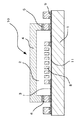
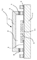
本発明が適用されるデバイス8を基板1上に配し、該基板1と金属製または半導体製のキャップ4の接合により形成される空間2内に上記デバイス8を内含するパッケージ構成10の一例を図1、2に示す。図1は基板側接合部6及びキャップ側接合部5の最表面に金属層を形成し、圧着または熱圧着により接合したものであり、図2は基板側接合部6及びキャップ側接合部5の最表面に金属層を形成し、ろう材7を接合材として用いて接合したものである。図1、2ともにキャップ4は導電性材料で構成されており、キャップ4が半導体製であってもオーミックコンタクトを介する事によりキャップ4の電位は基板側接合部6の金属層と等電位にすることが可能である。一方上記デバイス8として微小信号を扱う回路や可動部を有し、可動部の変位に連動した容量変化を検出することにより可動部の変位を検出する加速度センサや角速度センサやアクチュエータでは、信号レベルに比べて電気的外乱が大きく外乱が性能を損なう原因となる。
【0046】
本発明では、上記に説明したように基板1上に配されたデバイス8はキャップ4により覆われており、キャップ4は基板側接合部6の金属層と等電位にすることが可能であり、基板側接合部6の金属層は配線等を介して上記デバイス8の基準電位に対して一定の電位とすることが可能となる。そのため、電気的外乱に対するシールド効果をもたせることが可能である。よって電気的外乱による性能低下の少ない回路またはセンシングシステムの提供が可能となる。
【0047】
図1、2において基板1に導電体または半導体を用いることにより基板電位の制御が可能となり、基板1上に配されたデバイス8の基準電位に対して一定の電位に制御することにより電気的外乱に対するシールド効果が期待できる。デバイス8として微小信号を扱う回路や可動部を有し可動部の変位に連動した容量変化を検出することにより、可動部の変位を検出する加速度センサや角速度センサやアクチュエータでは電気的外乱による性能低下の少ない回路またはセンシングシステムの提供が可能となる。
【0048】
図1、2に示すように基板1とキャップ4より構成される空間2の内外を電気的に接続し、基板1及びキャップ4に対して電気的に絶縁された配線3を設けることにより上記空間2内への電力の供給及び上記空間2内で発生した信号の検出が可能となる。導電体または半導体基板1上に第1の絶縁層11を形成したものまたは非導電性基板上に配線層を形成し、配線層を含む基板上に第2の絶縁層9を形成し、基板1上に配置されたデバイス8を囲むように第2の絶縁層9上に直接または単結晶、多結晶または非晶質の半導体層を介して基板側接合部6を形成する。上記工程で、第2の絶縁層9または単結晶、多結晶または非晶質の半導体層の形成は通常の半導体プロセスである成膜、フォトリソ及びエッチングにより製造可能であり、基板に対して貫通電極を設け裏面より電極を取る。またはキャップ4側に貫通電極を設け、キャップ4上より電極をとる場合に比べて基板表面上のみの加工で済み、また、貫通電極形成時の穴埋めの信頼性の問題もなく低コスト、高歩留まりが可能となる。またこのことは、SOI基板を用いたマイクロマシンセンサ、マイクロマシンアクチュエータや電子回路にも適応される。
【0049】
図2に示す接合部のろう材7としてAuSn系合金を用いることにより、低温で接合でき接合部の多層膜間、接合部の多層膜と基板1またはキャップ4間の反応が抑制でき、信頼性の高い接合部が期待できる。また、AuSn系合金の融点ははんだ工程の温度より高いのでAuSn系合金を用いることによる特別な工程を必要とせずコスト上昇を抑制できる。
【0050】
上記図2に示す接合部のろう材7としてAuSn系合金を用いる場合、キャップ側接合部5と基板側接合部6の少なくとも一方の接合部の最表面にAu層を用いることにより接合部とAuSn系合金とのなじみが良くなり高い接合強度が期待できる。また、半導体プロセスを用いた可動部を有するデバイス8の形成には通常Si、SiO2、SiN、SiON等のSi系材料が用いられており、Siを可動部とするデバイス8ではSiO2上にSiを介して基板1に拘束した状態で目的の形状に加工し、最後にSiO2を除去することにより拘束から開放し可動できるようにする。なお、通常加速度センサや振動型角速度センサ等の可動部は一端が基板1に接続され、他端が可動部に接続されたばねとして働く梁により基板1上に保持され、静電モータ等梁で保持できない可動部は回転中心にSi等からなるピンを形成し基板1上に保持される。
【0051】
また、接合部の金属層の形成にはフォトリソ工程が必要であり、基板1上に感光レジスト膜を均一に形成する必要があり、基板表面の凹凸の少ない可動部の形状加工前に基板1上の金属層の形成は行われる。上記のように半導体プロセスを用いた可動部を有するデバイス8の形成には、通常SiO2の除去工程が必要であり、SiO2の除去にはバッファードフッ酸等のエッチャントを用いることが多く、基板1上の金属層の腐食を防ぐ工夫が必要である。しかし、本発明に示すように接合部の金属層の最表面をAu層とすると同時に接合部以外に用いられる基板1上の金属層の最表面をAu層とすることによりエッチャントに対する耐腐食性が向上しSiO2の除去時の工程の自由度があがる。
【0052】
図3に示すようにAuSn系合金のメッキ、印刷、融着、あるいは溶接等でろう材7をキャップ側接合部5上に形成することにより、接合時の部品点数の削減が可能となり、また、合わせ精度の向上が期待できる。
【0053】
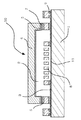
図5にはキャップ側接合部5の最表面をAu層とし、かつ、キャップ側接合部5以外の最表面も少なくとも一部Au層で形成し、キャップ側接合部5のAu層と連続した面を形成している。このような構造により、基板1とキャップ4の接合において、押し出されるAuSn系合金が、なじみの悪いSi系の基板形成材料に流れることなく、なじみのよいキャップ側接合部5以外の最表面のAu層に吸い上げられるため、デバイス8に影響を与えることを抑えることができる。このため、デバイス8と接合部間の距離を小さくすることができ、その結果、デバイス8全体を小型化できる。
【0054】
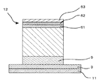
図6に示すように接合部の金属層の層構造12を基板側からAl/Ni/Auとすることにより、Al61と基板1間の密着強度が上がり、また、最表面にAu層63を形成することによりろう材7にAuSn系合金を用いた場合のろう材7とのなじみが良く接合強度が上がる。また、Al層61とAu層63の間にNi層62を設けることによりAl61とAu63間の反応を抑制でき耐熱性が向上する。さらに通常の半導体プロセスを用いた、可動部を有するデバイス8を基板1への拘束から開放する為に必要なSiO2層の除去において、書籍「フォトエッチングと微細加工」(樽岡、二瓶著、総合電子出版社)によるとSiO2層フッ酸系エッチャントでAl層61の腐食の抑制が可能であり、Au層63及びNi層62がフッ酸系エッチャントに対する耐腐食性が高いことより、SiO2層の除去時に基板側接合部6の特別な保護が不要となり、工程の簡易化による低コスト化、高歩留まりが期待できる。
【0055】
【発明の効果】
本発明によれば以上説明したように、ウェーハレベルパッケージの構造および製造方法は工程を簡便に構成でき、かつ使用部品のコスト低減を可能とされる構成となり、多大な効果を有する。
【0056】
上記した手段によれば、基板側接合部およびキャップ側接合部を金属で形成したので導電性を有し、それらの電位が安定し、外部電気的ノイズに対し影響されにくいデバイスとなる。このことは、マイクロメカニカルなデバイスで微小信号を扱うセンサーの場合においては好ましい構成となる。また金属で形成された基板側接合部およびキャップ側接合部は圧着により接合されるので、従来の低融点ガラスによる接合材に比べ、接合材が基板とキャップとの間に押し出される量が格段に減少し、接合部の面積を小さく構成できる。そして基板接合部とキャップ接合部はろう材で接合したことで接合強度が強くなる。また、ろう材に厚みを持たせれば、ウェハレベルの接合においても、基板ウェハ及びキャップウェハの歪を吸収することが可能となり歩留りを向上できる。ろう材に用いるAuSn系合金は比較的低温で溶融し、かつ鉛ハンダや鉛レスハンダの融点より高温であるので、パッケージ後のハンダ工程が可能となる。また、基板とキャップの接合時の融着温度を従来技術の構成よりも下げることが可能となるので、キャップ、ろう材、基板間の熱膨張率の違いにより生ずる歪も低減できる。また、基板側接合部の金属と基板との反応を抑制できる。
【0057】
さらには、基板側接合部のAu層よりろう材、キャップ側接合部の金属を介して、半導体製または金属製の前記キャップに外部より電位を印加できる構成となるので、導電性で構成される部位のマイクロメカニカルなデバイスの外部電気ノイズに対するシールド効果が高められる。このことは、マイクロメカニカルなデバイスが微小信号を扱うセンサートの場合では、非常に大きな利点となる。
【0058】
通常マイクロメカニカルなデバイスは、SiO2等の表面組織に対して選択的にエッチング可能な被エッチング層を介して基板上に形成され、製造工程の最後に上記被エッチング層をエッチング除去して、マイクロメカニカルなデバイスを可動とする。本請求項では、接合部材の金属形成後キャップ接合前に上記被エッチング層であるSiO2層を除去する際に、SiO2のエッチャントに対して耐腐食性のある金属層よりなるため、SiO2層の除去時に金属層の保護手段を講じる必要がなく、工程の低コスト化が可能である。また、Alは反応性が高く、基板側との密着性が良いし、AuはAuSn系合金ろう材とのなじみが良い。しかし、AlとAuは低温で反応し反応層より剥離を生ずることは公知である。本請求項では、AlとAu間の反応防止膜としてNi層を挿入し、基板側ともAuSn系合金ろう材とも密着性が良く、かつ、耐熱性の高い金属層を形成できる。
【図面の簡単な説明】
【図1】本発明の実施の形態における概略的なパッケージの構成を示す断面図である。
【図2】本発明の別の実施の形態におけるパッケージの概略的な断面図である。
【図3】本発明の実施の形態におけるパッケージ構成であって、ろう材としてAuSn系合金をメッキ、印刷、溶着、溶接等によりキャップ側接合部上に形成した、図2の接合前の概略的な断面図である。
【図4】本発明の実施の形態においてプリフォーム状のろう材を用いた場合の図2の接合前の状態を示す概略的な断面図である。
【図5】本発明の実施の形態におけるキャップ側表面にAu層を形成する場合の概略的な断面図である。
【図6】本発明に係る本発明の実施の形態における基板側接合部の金属層の構造を概略的に示した断面図である。
【符号の説明】
1:基板
2:空間
3:配線
4:キャップ
5:キャップ側接合部
6:基板側接合部
7:ろう材
8:デバイス
9:第2の絶縁層
10:表面組織を基板上に配し、該基板と金属製または半導体製のキャップの接合により形成される空間内に前記表面組織を内含するパッケージ構成
11:第1の絶縁層
12:基板側接合部の金属層の構造
61:基板側接合部のAl層
62:基板側接合部のNi層
63:基板側接合部のAu層[0001]
TECHNICAL FIELD OF THE INVENTION
The present invention relates to a configuration and a manufacturing method of a micromachine package having a substrate, a micromechanical device having a movable portion formed on the substrate, and a cap for covering the device, which is manufactured using a micromachining technique.
[0002]
[Prior art]
Conventionally, a ceramic package or the like having a space in the package has been used for a package of a substrate of a micromechanical device having a movable portion.
[0003]
As an improved technique, for example, there is a package used as an accelerometer having a structure in which a device is hermetically sealed in a cavity having a predetermined size by a combination of a semiconductor substrate wafer, a cap wafer, and frit glass. The disclosed configuration is a semiconductor wafer level package that encapsulates devices manufactured on a semiconductor substrate wafer before dicing the semiconductor substrate wafer into individual chips. The cap wafer, which is part of the semiconductor wafer level package, and a predetermined pattern of frit glass used as a bonding material are bonded to the semiconductor substrate wafer so that the device is hermetically sealed in the cavity. The electrodes that extend through the frit glass seal and connect to the device are configured to allow electrical connection by holes in the cap wafer. (For example, see Patent Document 1)
Another method is disclosed for packaging a surface structure before dicing a substrate wafer on which a surface structure including wirings and elements is arranged. In this refinement, a cap wafer is formed by a glass wafer with a structural element comprising at least one micromechanical surface texture structured on a silicon substrate and one cap covering the at least one surface texture. The structure that is formed is described. (For example, see Patent Document 2)
[0004]
[Patent Document 1]
Patent No. 3303146
[0005]
[Patent Document 2]
JP-T-2002-500961
[0006]
[Problems to be solved by the invention]
However, the above-mentioned known techniques have the following problems. The use of the above ceramic package makes it difficult to reduce the size.If a separate circuit is required, a dedicated package or a separate circuit is required, which leads to an increase in the size and cost of a system having the above devices. I was copying.
[0007]
Furthermore, in order to arrange the above device and seal it in a ceramic package, it is necessary to cut out and handle the substrate wafer in a state where the device is exposed, and it may cause electrical leakage due to chips, mechanical malfunction, handling error. The yield was reduced due to damage.
[0008]
The bonding strength between the low melting point frit glass, which is the bonding material of
[0009]
In order to apply the frit glass to the cap wafer, the cap wafer, the frit glass, and the semiconductor substrate wafer are heated and fused. However, since the frit glass is formed by printing, the surface has irregularities. In addition, since the frit glass has a high viscosity at the bonding temperature, the bonding area must be increased, and in these bondings, the cap wafer and the semiconductor substrate wafer are heat-fused in a pressurized state. There must be. As a result, there is a disadvantage that a specific amount of the low-melting glass is inevitably extruded and spread between the semiconductor substrate wafer and the cap wafer.
[0010]
In order to avoid the device being affected by this extruded low melting glass, it is necessary to ensure a relatively large bonding area between the semiconductor substrate wafer and the cap wafer, so that the device is correspondingly It gets bigger.
[0011]
In addition, since the low-melting glass is interposed at the joint between the semiconductor substrate wafer and the cap wafer, conduction between the semiconductor substrate wafer and the cap wafer cannot be established, and the potential of the cap wafer becomes unstable due to the influence of external electric noise. In a sensor in which a device handles a small signal, the device is affected by the unstable potential of the cap wafer, which causes a deterioration in sensor performance. Further, another manufacturing process is required to stabilize the potential of the cap wafer, which causes an increase in cost.
[0012]
In
[0013]
Therefore, the present invention has been made in view of the above problems, and has as its technical object to provide a structure and a manufacturing method of a micromachine package that is resistant to external electric noise and that can be reduced in size and cost. .
[0014]
[Means for Solving the Problems]
The technical measures taken to solve the above-mentioned problems include a substrate, a device in which a movable portion is formed on the substrate, or a device which is deformed by an externally applied signal, a first wiring, a metal, In a package structure including a semiconductor cap and a device disposed in a space formed by the substrate and the cap, the substrate-side joint formed on the substrate and the cap-side joint formed on the cap are formed of metal. That is.
[0015]
According to the above-described means, since the substrate-side joint and the cap-side joint are formed of a conductive metal, the device is less susceptible to external electrical noise. This is a preferable configuration in the case of a sensor that handles a small signal with a micromechanical device.
[0016]
Further, a technical measure taken in
[0017]
According to the above-described means, the substrate-side joining portion and the cap-side joining portion formed of metal are joined by pressure bonding, so that the joining material is located between the substrate and the cap as compared with the conventional joining material made of low-melting glass. The amount of extrusion is significantly reduced, and the area of the joint can be reduced.
[0018]
A technical measure taken in
[0019]
According to the above-described means, the joining strength is increased by joining the substrate joining portion and the cap joining portion with the brazing material. Further, if the brazing material has a thickness, it is possible to absorb the distortion of the substrate wafer and the cap wafer even at the wafer-level bonding, thereby improving the yield. This is an advantage in miniaturization.
[0020]
A technical measure taken in
[0021]
According to the above-described means, the AuSn-based alloy is melted at a relatively low temperature and has a temperature higher than the melting point of lead solder or lead-less solder, so that a soldering step after packaging becomes possible. Further, since the fusion temperature at the time of joining the substrate and the cap can be lowered, distortion caused by a difference in thermal expansion coefficient between the cap, the brazing material, and the substrate can also be reduced. In addition, the reaction between the metal of the substrate-side joint and the substrate can be suppressed. In addition, even when a plurality of types of metals have a laminated structure, it is possible to suppress a reaction between different types of metals, and it is possible to increase the selectivity of the metal at the substrate-side joint.
[0022]
The technical measure taken in
[0023]
According to the above-described means, the Au layer is extremely less deteriorated by the reaction with the outside air than other metals, and is easy to store and manage in manufacturing. Further, since it is inert to many chemicals such as acids, alkalis and organic solvents, the degree of freedom of chemical treatment of the substrate before bonding is increased. Further, since there is little deterioration due to the reaction with the outside air when the substrate and the cap are joined in the atmosphere of the melting temperature of the brazing material, the joining quality can be stabilized.
[0024]
The technical measures taken in
[0025]
According to the above-described means, the brazing material extruded between the substrate and the cap is poorly compatible with the substrate and members other than the bonding portion on the substrate, and is well compatible with the Au layer on the outermost surface on the cap side. Therefore, the extent to which the device is absorbed by the Au layer on the cap side and affects the device can be extremely suppressed.
[0026]
A technical measure taken in
[0027]
According to the above-described means, in the alignment at the time of joining the substrate and the cap, the brazing material is fixed in advance by fusion or welding according to the shape of the joining portion, so that the accuracy of positioning can be improved.
[0028]
A technical measure taken in
[0029]
According to the above-described means, the accuracy of alignment at the time of joining can be improved, similarly to the technical means taken in
[0030]
A technical measure taken in
[0031]
According to the above-described means, the Au layer is extremely less deteriorated by the reaction with the outside air than other metals, and is easy to store and manage in manufacturing. Further, since it is inert to many chemicals such as acids, alkalis and organic solvents, the degree of freedom of chemical treatment of the substrate before bonding is increased. Further, since there is little deterioration due to the reaction with the outside air when the substrate and the cap are joined in the atmosphere of the melting temperature of the brazing material, the joining quality can be stabilized.
[0032]
According to a tenth aspect of the present invention, the Au layer on the outermost surface of the substrate-side junction is configured to be capable of externally applying a potential.
[0033]
According to the above-described means, the semiconductor or metal cap can be externally applied with an electric potential via the brazing material and the metal of the cap-side junction from the Au layer of the substrate-side junction, so that the conductive property is improved. The shielding effect against external electric noise of the micromechanical device in the portion constituted by the above is enhanced. This is a great advantage in the case where the micromechanical device is a sensor handling small signals.
[0034]
A technical measure taken in
[0035]
According to the above-described means, since the space formed by the substrate and the cap is surrounded by the same potential, reduction of electrical noise can be expected. Further, in the device on the substrate, since the cap and the substrate are electrically connected, it is not necessary to intentionally apply a cap potential, which leads to cost reduction.
[0036]
According to a twelfth aspect of the present invention, there is provided a second wiring which is electrically insulated from the substrate, the cap, and the cap joint and electrically connects the inside and the outside of the space.
[0037]
According to the above-described means, the internal micromechanical device is driven by an electric signal from the outside by the second wiring sealed between the cap and the substrate and electrically connecting the inside and the outside of the space. Is possible. It is also possible to sense the displacement of the internal device as a change in capacitance, a change in resistance, a change in potential, or a change in current. This is advantageous for actuators and sensors that require displacement of the internal micromechanical device.
[0038]
14. The technical means according to claim 13, wherein the first wiring or an upper layer of a second wiring formed on a substrate made of a conductor or a semiconductor via a first insulating layer made of a single layer or a multilayer. And a second insulating layer composed of a single layer or a multilayer made of a material different from the outermost layer of the non-conductive substrate or the first insulating layer, and a substrate side joint is formed on the second insulating layer. That was done.
[0039]
According to the above-described means, usually, a micromechanical device is formed on a substrate via a layer to be etched which can be selectively etched with respect to a device such as SiO2, and the layer to be etched is formed at the end of a manufacturing process. Etching is removed to make the micromechanical device movable. In the above claim, since the second insulating layer is made of a material different from the outermost layer of the non-conductive substrate or the first insulating layer, the etching of the device, the non-conductive substrate or the first insulating layer is performed. The influence can be suppressed, and only the second insulating layer can be removed by etching. In addition, it is possible to form a combination of a plurality of electrically separated functions between the device, the wiring, and the substrate.
[0040]
A technical measure taken in claim 14 is that the substrate has a single-crystal, polycrystalline or amorphous semiconductor layer via at least one insulating layer, and a substrate-side junction is formed on the semiconductor layer. It is.
[0041]
According to the above-described means, for example, since the adhesion of the metal to the semiconductor layer is higher than the adhesion of the metal layer to the insulating layer of the Si oxide film and the Si nitride film, the substrate-side junction is formed on the semiconductor layer. This increases the bonding strength and improves the sealing reliability. Further, similarly to the thirteenth aspect, it is possible to form a combination of a plurality of electrically separated functions between the wiring and the substrate.
[0042]
A technical measure taken in claim 15 is that the metal layer at the substrate side joint is made of Au, Ni and Al from the surface layer.
[0043]
According to the above-described means, usually, the micromechanical device is formed on the substrate via the layer to be etched which can be selectively etched with respect to a surface structure such as
[0044]
BEST MODE FOR CARRYING OUT THE INVENTION
Hereinafter, embodiments of the present invention will be described with reference to the drawings.
[0045]
An example of a
[0046]
In the present invention, as described above, the
[0047]
1 and 2, the use of a conductor or a semiconductor for the
[0048]
As shown in FIGS. 1 and 2, the inside and outside of a
[0049]
By using an AuSn-based alloy as the
[0050]
In the case where an AuSn-based alloy is used as the
[0051]
In addition, a photolithography process is required to form the metal layer at the bonding portion, and it is necessary to uniformly form a photosensitive resist film on the
[0052]
As shown in FIG. 3, by forming the
[0053]
In FIG. 5, the outermost surface of the cap-
[0054]
As shown in FIG. 6, by making the
[0055]
【The invention's effect】
According to the present invention, as described above, the structure and manufacturing method of a wafer-level package can be configured with a simple process and can reduce the cost of parts to be used.
[0056]
According to the above-described means, since the substrate-side junction and the cap-side junction are formed of metal, the device has conductivity, has a stable electric potential, and is hardly affected by external electric noise. This is a preferable configuration in the case of a sensor that handles a small signal with a micromechanical device. Also, since the board-side joint and the cap-side joint made of metal are joined by crimping, the amount of the joining material pushed out between the substrate and the cap is significantly higher than that of the conventional joining material made of low-melting glass. The joint area can be reduced. The joining strength between the substrate joining portion and the cap joining portion is increased by joining with the brazing material. Further, if the brazing material has a thickness, it is possible to absorb the distortion of the substrate wafer and the cap wafer even at the wafer-level bonding, thereby improving the yield. The AuSn-based alloy used for the brazing material is melted at a relatively low temperature and has a temperature higher than the melting point of lead solder or lead-less solder, so that a soldering step after packaging can be performed. Further, since the fusion temperature at the time of joining the substrate and the cap can be made lower than that of the prior art, the distortion caused by the difference in the coefficient of thermal expansion between the cap, the brazing material, and the substrate can also be reduced. In addition, the reaction between the metal of the substrate-side joint and the substrate can be suppressed.
[0057]
Further, since the structure is such that a potential can be externally applied to the semiconductor or metal cap via the brazing material and the metal of the cap side bonding part from the Au layer of the substrate side bonding part, the conductive layer is made of a conductive material. The shielding effect against external electric noise of the micromechanical device at the site is enhanced. This is a great advantage in the case where the micromechanical device is a sensor handling small signals.
[0058]
Usually, a micromechanical device is formed on a substrate via an etching target layer which can be selectively etched with respect to a surface structure such as SiO2. At the end of the manufacturing process, the above etching target layer is removed by etching to obtain a micromechanical device. Make the device movable. In the present invention, when the SiO2 layer, which is the layer to be etched, is removed after forming the metal of the joining member and before the cap joining, the SiO2 layer is made of a metal layer having corrosion resistance to the etchant of SiO2. Sometimes, it is not necessary to take measures for protecting the metal layer, and the cost of the process can be reduced. Al has high reactivity and good adhesion to the substrate side, and Au has good compatibility with the AuSn alloy brazing material. However, it is known that Al and Au react at a low temperature and peel off from the reaction layer. In the present invention, a Ni layer is inserted as an anti-reaction film between Al and Au, so that a metal layer having good adhesion to both the substrate and the AuSn-based alloy brazing material and having high heat resistance can be formed.
[Brief description of the drawings]
FIG. 1 is a cross-sectional view showing a schematic configuration of a package according to an embodiment of the present invention.
FIG. 2 is a schematic cross-sectional view of a package according to another embodiment of the present invention.
3 is a schematic view of a package configuration according to an embodiment of the present invention, in which an AuSn-based alloy is formed as a brazing material on a cap-side joint portion by plating, printing, welding, welding, or the like, and before joining in FIG. 2; FIG.
FIG. 4 is a schematic cross-sectional view showing a state before joining of FIG. 2 when a preform brazing material is used in the embodiment of the present invention.
FIG. 5 is a schematic cross-sectional view when an Au layer is formed on a cap-side surface according to the embodiment of the present invention.
FIG. 6 is a cross-sectional view schematically showing a structure of a metal layer at a substrate-side joint according to an embodiment of the present invention.
[Explanation of symbols]
1: substrate
2: Space
3: Wiring
4: Cap
5: Cap side joint
6: Board side joint
7: brazing filler metal
8: Device
9: second insulating layer
10: Package structure in which a surface texture is arranged on a substrate and the surface texture is included in a space formed by joining the substrate and a metal or semiconductor cap.
11: first insulating layer
12: Structure of the metal layer at the substrate side joint
61: Al layer on the substrate side joint
62: Ni layer at the substrate side joint
63: Au layer at substrate-side junction
Claims (15)
Priority Applications (1)
| Application Number | Priority Date | Filing Date | Title |
|---|---|---|---|
| JP2002372417A JP2004202604A (en) | 2002-12-24 | 2002-12-24 | Package structure and manufacturing method |
Applications Claiming Priority (1)
| Application Number | Priority Date | Filing Date | Title |
|---|---|---|---|
| JP2002372417A JP2004202604A (en) | 2002-12-24 | 2002-12-24 | Package structure and manufacturing method |
Publications (1)
| Publication Number | Publication Date |
|---|---|
| JP2004202604A true JP2004202604A (en) | 2004-07-22 |
Family
ID=32811029
Family Applications (1)
| Application Number | Title | Priority Date | Filing Date |
|---|---|---|---|
| JP2002372417A Pending JP2004202604A (en) | 2002-12-24 | 2002-12-24 | Package structure and manufacturing method |
Country Status (1)
| Country | Link |
|---|---|
| JP (1) | JP2004202604A (en) |
Cited By (7)
| Publication number | Priority date | Publication date | Assignee | Title |
|---|---|---|---|---|
| JP2007042786A (en) * | 2005-08-02 | 2007-02-15 | Sony Corp | Micro device and its packaging method |
| JP2007214438A (en) * | 2006-02-10 | 2007-08-23 | Dainippon Printing Co Ltd | Sensor package |
| JP2007214441A (en) * | 2006-02-10 | 2007-08-23 | Dainippon Printing Co Ltd | Composite sensor package |
| JP2008039435A (en) * | 2006-08-01 | 2008-02-21 | Mitsubishi Electric Corp | Acceleration sensor |
| JP2009516365A (en) * | 2005-11-10 | 2009-04-16 | フラウンホーファー・ゲゼルシャフト・ツール・フェルデルング・デア・アンゲヴァンテン・フォルシュング・エー・ファウ | Cover wafer or structural element-cover, wafer structural part or structural element usable for microtechnology, and corresponding wafer-part or structural element-part soldering method |
| WO2010004766A1 (en) * | 2008-07-11 | 2010-01-14 | ローム株式会社 | Mems device |
| US9985599B2 (en) | 2012-05-18 | 2018-05-29 | Murata Manufacturing Co., Ltd. | Quartz vibrator manufacturing method and quartz vibrator |
-
2002
- 2002-12-24 JP JP2002372417A patent/JP2004202604A/en active Pending
Cited By (10)
| Publication number | Priority date | Publication date | Assignee | Title |
|---|---|---|---|---|
| JP2007042786A (en) * | 2005-08-02 | 2007-02-15 | Sony Corp | Micro device and its packaging method |
| JP2009516365A (en) * | 2005-11-10 | 2009-04-16 | フラウンホーファー・ゲゼルシャフト・ツール・フェルデルング・デア・アンゲヴァンテン・フォルシュング・エー・ファウ | Cover wafer or structural element-cover, wafer structural part or structural element usable for microtechnology, and corresponding wafer-part or structural element-part soldering method |
| US8039950B2 (en) | 2005-11-10 | 2011-10-18 | Fraunhofer-Gesellschaft Zur Foerderung Der Angewandten Forschung E.V. | Solder material lining a cover wafer attached to wafer substrate |
| KR101416773B1 (en) | 2005-11-10 | 2014-08-06 | 프라운호퍼-게젤샤프트 츄어 푀르더룽 데어 안게반텐 포르슝에.파우. | Cover wafer or component cover, wafer part or component that can be inserted using microsystems technology, and soldering method for connecting corresponding wafer or component parts |
| JP2007214438A (en) * | 2006-02-10 | 2007-08-23 | Dainippon Printing Co Ltd | Sensor package |
| JP2007214441A (en) * | 2006-02-10 | 2007-08-23 | Dainippon Printing Co Ltd | Composite sensor package |
| JP2008039435A (en) * | 2006-08-01 | 2008-02-21 | Mitsubishi Electric Corp | Acceleration sensor |
| WO2010004766A1 (en) * | 2008-07-11 | 2010-01-14 | ローム株式会社 | Mems device |
| JP5769964B2 (en) * | 2008-07-11 | 2015-08-26 | ローム株式会社 | MEMS device |
| US9985599B2 (en) | 2012-05-18 | 2018-05-29 | Murata Manufacturing Co., Ltd. | Quartz vibrator manufacturing method and quartz vibrator |
Similar Documents
| Publication | Publication Date | Title |
|---|---|---|
| JP3644205B2 (en) | Semiconductor device and manufacturing method thereof | |
| JP4012886B2 (en) | Manufacturing method of micro electro mechanical system using solder balls | |
| JP5892378B2 (en) | Manufacturing method of package material | |
| JP2008046078A (en) | Micro electromechanical system element and manufacturing method thereof | |
| US20160297675A1 (en) | Semiconductor device, and method of manufacturing device | |
| JP5330697B2 (en) | Functional element package and manufacturing method thereof | |
| WO2008023465A1 (en) | Microelectronic machine mechanism device, and its manufacturing method | |
| KR100757695B1 (en) | Component and method for manufacture | |
| KR20030077754A (en) | Micro inertia sensor and method thereof | |
| JP5610177B2 (en) | Functional device and manufacturing method thereof | |
| WO2007074846A1 (en) | Microelectronic machine and method for manufacturing same | |
| JP2009016717A (en) | Semiconductor device and method of manufacturing the same | |
| JP7408764B2 (en) | MEMS elements and MEMS modules | |
| US20080128839A1 (en) | Electronic Apparatus Applied Anodic Bonding | |
| JP2004202604A (en) | Package structure and manufacturing method | |
| JP3702062B2 (en) | Pressure sensor device | |
| JP2009533861A (en) | Method for manufacturing electronic assembly, electronic assembly, cover and substrate | |
| JP2005228863A (en) | Semiconductor device, manufacturing method thereof and sensor | |
| JP4964505B2 (en) | Semiconductor device, manufacturing method thereof, and electronic component | |
| JP6773089B2 (en) | device | |
| EP1752734A2 (en) | Semiconductor device | |
| TWI564239B (en) | Process for producing a silicon intermediate carrier | |
| JP4353118B2 (en) | Signal extraction structure for semiconductor microelectromechanical devices | |
| JP5578803B2 (en) | Wafer package and manufacturing method thereof | |
| JP4404647B2 (en) | Electronic device and electronic component sealing substrate |
Legal Events
| Date | Code | Title | Description |
|---|---|---|---|
| A621 | Written request for application examination |
Free format text: JAPANESE INTERMEDIATE CODE: A621 Effective date: 20051125 |
|
| A131 | Notification of reasons for refusal |
Free format text: JAPANESE INTERMEDIATE CODE: A131 Effective date: 20081118 |
|
| A977 | Report on retrieval |
Free format text: JAPANESE INTERMEDIATE CODE: A971007 Effective date: 20081120 |
|
| A02 | Decision of refusal |
Free format text: JAPANESE INTERMEDIATE CODE: A02 Effective date: 20090310 |