【0001】
【産業上の利用分野】
本発明は静電搬送装置、現像装置、プロセスカートリッジ及び画像形成装置に関する。
【0002】
【特許文献1】特開2001ー139144号公報
【特許文献2】特開2002ー341656号公報
【従来の技術】
複写装置、プリンタ、ファクシミリ等の画像形成装置として、電子写真プロセスを用いて、潜像担持体に潜像を形成し、この潜像に粉体である現像剤(以下「トナー」ともいう。)を付着させて現像してトナー像として可視像化し、このトナー像を記録媒体(中間転写部材を含む。)に転写することで画像を形成するものがある。
【0003】
このような画像形成装置において、トナーを搬送するトナー搬送装置としては、回転自在なスクリューを用いたものが一般的であった。例えばパイプ内のトナーをパイプ内部に沿って設けられたスクリューを回転させることによって上記スクリューの軸線方向に搬送するものが知られている。
【0004】
しかしながら、このようなトナー搬送装置にあっては、パイプ内のスクリューを回転させるには比較的大きなモータを用い駆動するため装置面積が大型化となり、かつ回転音も大きいという問題がある。また、パイプ内壁とスクリューとの間にトナーが詰まると、摩擦熱により溶融し、トルクの増加や搬送不良を生じることがある。
【0005】
一方、その他のトナー搬送装置としては、トナーに空気流を当てたり巻き込むことによりトナーを空気流とともに搬送する装置、振動によりトナーが傾斜に沿って滑り落ちるのを助けトナーを搬送する装置、帯電したトナーを電界により搬送する装置等も知られている。
【0006】
これらのうち、トナーを空気流とともに搬送する装置にあっては、微少な粒子状物体の搬送密度は空気で薄められて疎になり低効率な搬送方法である。また、振動によって搬送を助けるトナーを搬送する装置にあっては、振動を起こさせるために比較的大きなエネルギーが必要であり、搬送方向も重力方向に限られるという不都合が生じている。
【0007】
そこで、上述した電界を用いて帯電トナーを搬送する装置は、機械的部分の摩耗や振動を伴わないので、騒音の伴わず、長期的安定した画像形成動作を維持することが可能となり、このような搬送装置としては
【特許文献1】や
【特許文献2】などに開示されている。
【0008】
この電界を用いた一般的なトナー搬送装置について図38及び図39を参照して説明する。なお、図38は同トナー搬送装置の平面説明図、図39はその搬送電極部分の断面説明図である。
【0009】
このトナー搬送装置は、絶縁体からなる支持基板501上に所定の電極幅を有する薄膜からなる搬送電極502を所定の電極間隔で多数本配置し、その表面には短絡防止のための絶縁膜503を形成して搬送電極502をカバーし、絶縁膜503の表面を搬送面504とする搬送基板500を構成している。そして、支持基板501には搬送電極502…の一端部側に給電電極505a、505b、505cを設けている。なお、
【特許文献1】では各給電電極505a、505b、505c、搬送電極502はそれぞれ絶縁膜を介して積層された構造としている。
【0010】
ここで、給電電極505a、505b、505cを介して搬送電極502に対して例えば3相のそれぞれ位相のずれた駆動電圧(駆動信号)va、vb、vcを供給して進行波電界を発生させることにより、その電界の作用により帯電トナーを図38で矢印方向に搬送させることができる。
【0011】
このようなトナー搬送装置においては、電界によるトナーの搬送を精度よく行うために、一つの電極上からトナーを離間させ、更に他の電極上に停止するようなトナーの移動制御を行わなければならず、また、すべての電極において上記の移動制御を行わなければならない。
【0012】
ところで、搬送基板上に、幅が0.01〜1mm程度の線状の搬送電極を0.01〜1mm程度の間隔で多数本、櫛状にフォトリソグラフィー技術を用いて一列に並べて形成するが、この場合、電極幅については、トナーに対する電界による制御の観点からは粒径との整合を取る必要があり、また、低電圧駆動の観点からは、幅が狭いことが好ましい。
【0013】
しかしながら、電極形成において幅の狭い搬送電極を数千本形成する場合、いかにクリーンルーム環境化において形成しても、無欠陥を選るには難しいものがあり、断線等の欠陥が発生するおそれがある。このような搬送電極の一部が断線を生じた場合、例えば図40に示すように、1本の搬送電極502の途中で断線510が発生した場合、断線510の箇所から先の部分には電圧を供給することができず、その搬送電極502の先の部分には電界が発生しなくなるので、トナーが断線した手前の搬送電極で停止してしまい、トナー溜まり511が生じることになり、後続のトナーも搬送されなくなる。
【0014】
また、従来の電界によるトナー搬送装置においては、搬送すべきトナー中に凝集した比較的粗大化した粒子が存在した場合、搬送基板との接触面積が増加することとなり、これらの粒子に対する進行波電界による搬送性が悪く欠陥部分で停止状態となる。
【0015】
このように搬送基板上でトナーが停止した場合には、停止したトナーが搬送路を塞ぐことになり、他のトナーの搬送を妨害することとなるため、搬送性の低下や、搬送不良が発生することとなり、良好な顕像化が得られにくくなる。
【0016】
この場合、帯電トナーの搬送不良を防ぐ手段として、各搬送電極に印加する信号電圧を上げ、発生する電界強度を上げて搬送力を増すことが考えられるが、搬送電極の寿命低下、あるいは各搬送電極間のより高絶縁耐圧化を考慮する必要がある。
【0017】
そこで、
【特許文献1】に記載の搬送装置にあっては、搬送電極と空隙をおいて対向配置する対向電極を設け、搬送電極と対向電極間に交番電界を発生させて、この交番電界によって帯電したトナーを搬送電極と対向電極間で飛翔させることにより、搬送電極間にて発生する進行波電界でトナーを搬送方向に搬送させるようにしている。
【0018】
【発明が解決しようとする課題】
しかしながら、上述した
【特許文献1】に記載されているように搬送基板の搬送電極と所定の間隔をおいて対向する対向電極で交番電界を発生させるようにするためには、帯電トナーを搬送する搬送電極に駆動電圧を入力する搬送入力電源の他に、帯電トナーを搬送電極と対向電極間で飛翔させるための交番電界を発生させるための電源を設けなければならず、構成が複雑になる。
【0019】
また、前述したように搬送電極の長手方向にて断線した場合、搬送入力電源との接続側は電圧が供給されるが、断線箇所より先の部分には電圧が供給されないため、トナーが電極上に固着するおそれがあり、対向電極による交番電界を用いたとしても、上記同様搬送性が悪く、欠陥部分で滞留状態となる。
【0020】
さらに、このように対向電極を用いる構成では、本出願人が
【特許文献2】で開示したようなETH現像に適用することができない。なお、ETH(イース:Electrostatic Transport& Hopping)現象とは、粉体が移相電界のエネルギーを与えられ、そのエネルギーが機械的なエネルギーに変換されて、粉体自身が動的に変動する現象をいう。このETH現象は、静電気力による粉体の水平方向(搬送面に沿う方向の意味)の移動(搬送)と垂直方向(搬送面鉛直方向の意味)の移動(ホッピング)を含む現象であり、静電搬送基板の表面を、移相電界によって粉体が進行方向の成分を持って飛び跳ねる現象である。このETH現象を利用した現像をETH現像と称する。
【0021】
そこで、本発明者らは、
【特許文献1】に記載されているようなトナーの水平方向搬送を前提とする従来の静電搬送装置だけでなく、ETH現像にも適用できる静電搬送装置にも適用可能な解決手段を見出すため鋭意検討した結果、本発明をなすに至ったものであり、簡単な構成で粉体を安定して移動させることができる静電搬送装置、この静電搬送装置を用いた現像装置、プロセスカートリッジ、画像形成装置を提供することを目的とする。
【0022】
上記の課題を解決するため、本発明に係る静電搬送装置は、支持基板上に粉体を移動させる静電力を発生するための搬送電極が所定の間隔で略平行に移動方向と略直交する方向に繰り返し形成し配置され、更に表面に絶縁部材からなる搬送面が形成された搬送基板を有し、この搬送基板には搬送電極の両端部にて相互接続される共通電極が形成されている構成とした。なお、本明細書において、「粉体」とは、「粒子」、「微粒子」、「粉末」、「微粉末」、「粉体」、「微粉体」などを含む意味で用いる。
【0023】
ここで、搬送電極の両端部にて相互接続される共通電極にはn相(nは3以上の整数)の駆動信号印加用入力端子が設けられていることが好ましく、この場合搬送電極と相互接続される両側の共通電極の一方側には駆動信号印加用入力端子が設けられ、他方側には駆動信号印加用入力端子が設けられていない構成とすることができる。また、駆動信号印加用入力端子は移動方向と直交する方向で共通電極よりも外側に引き出された位置に配置されている構成とすることができる。
【0024】
また、n相の共通電極と各共通電極に接続される搬送電極とは異なる層にある構成とすること、或いは、共通電極及びこの共通電極に接続される搬送電極はn相のうちの少なくとも2相は相毎に同じ層にある構成とすることができる。
【0025】
さらに、両側の共通電極は搬送電極以外の低抵抗のパターンで相互接続されている構成とすることができる。また、共通電極は搬送電極よりも電極幅が広いことが好ましい。
【0026】
さらにまた、一体形成で相互接続された共通電極とこの共通電極に接続される搬送電極とを含み、あるいは、コンタクトホールを介して相互接続された共通電極とこの共通電極に接続される搬送電極とを含む構成とすることができる。このコンタクトホールを用いた相互接続の場合には、支持基板表面から共通電極、搬送電極の順に積層されていることが好ましい。
【0027】
また、共通電極と搬送電極とは支持基板の異なる表面側に設けることができる。さらに、搬送面を対向配置した少なくとも2枚の搬送基板を備えることができる。
【0028】
本発明に係る現像装置は、帯電トナーを移動させる本発明に係る静電搬送装置の搬送基板を備えている構成とした。
【0029】
本発明に係るプロセスカートリッジは、本発明に係る現像装置を含む構成とした。
【0030】
本発明に係る画像形成装置は、本発明に係る現像装置を備え、或いはプロセスカートリッジを複数備えている構成とした。
【0031】
【発明の実施の形態】
以下、本発明の実施の形態を添付図面を参照して説明する。先ず、本発明に係る静電搬送装置の第1実施形態について図1ないし図5を参照して説明する。なお、図1は同静電搬送装置の搬送基板の平面説明図、図2は図1のA−A線に沿う断面説明図、図3は図1のB−B線に沿う断面説明図、図4は図1のC−C線に沿う断面説明図、図5は図1のD−D線に沿う断面説明図である。
【0032】
この静電搬送装置は、粉体であるトナーを搬送及びホッピングさせるための電界を発生する複数の電極を有する搬送基板1を有し、この搬送基板1には図示しない駆動回路からn相(nは3以上の整数)の駆動信号Va(a相)、Vb(b相)、Vc(c相)が入力される。なお、ここでは、搬送基板1としてETH現
象を発生させる搬送基板で説明するが、前述した
【特許文献1】に開示されているように粉体を水平方向にだけ移動させる搬送基板にも同様に適用することができる。
【0033】
この搬送基板1は、ベース基板(支持基板)11上に3本の電極(搬送電極)12a、12b、12c(これらを「搬送電極12」と総称する。)を1セットとて、所定の間隔で、粉体移動方向に沿って粉体移動方向と略直交する方向に繰り返し形成配置し、更にその表面に無機又は有機の絶縁性材料で形成した絶縁部材からなる表面保護層13を形成し、この表面保護層13の表面を搬送面14としている。なお、ここでは、表面保護層13が搬送面14を形成する表面層となるが、表面保護層13上に更に粉体との適合性に優れた表面層を別途成膜することもできる。
【0034】
そして、これらの搬送電極12a、12b、12cの両側には、搬送電極12a、12b、12cとそれぞれ両端部で相互接続した共通電極15a、15b、15c(これらを「共通電極15」と総称する。)を粉体移動方向に沿って、すなわち、個々の搬送電極と略直交する方向に設けている。この場合、共通電極15の幅(この幅は、粉体移動方向と直交する方向の幅)は搬送電極12の幅(この幅は、粉体移動方向に沿う方向の幅)よりも広くしている。
【0035】
さらに、これらの共通電極15a、15b、15cの両端部にはそれぞれ駆動信号Va、Vb、Vcを入力するための駆動信号印加用入力端子16a、16b、16c(これらを「駆動信号印加用入力端子16」と総称する。)を設けている。
【0036】
ここで、支持基板11としては、ガラス基板、樹脂基板或いはセラミックス基板等の絶縁性材料からなる基板、或いは、SUSなどの導電性材料からなる基板にSiO2等の絶縁膜を成膜したもの、また、ポリイミドフィルムなどのフレキシブルに変形可能な材料からなる基板などを用いることができる。
【0037】
また、搬送電極12及び共通電極15の電極材料としては、Al、NiーCr等の導電性材料を用いることができ、これをフォトリソ技術等を用いて所要の電極形状にパターン化して形成している。また、搬送電極12の粉体進行方向における幅は移動させる粉体の平均粒径の1倍以上20倍以下とし、かつ、搬送電極12、12の粉体進行方向の間隔も移動させる粉体の平均粒径の1倍以上20倍以下としている。
【0038】
表面層13としては、例えばSiO2、TiO2、TiO4、SiON、BN、TiN、Ta2O5などを用いることができる。また、無機ナイトライド化合物、例えばSiN、Bn、Wなどを用いることができる。特に、表面水酸基が増えると帯電粉体の帯電量が搬送途中で下がる傾向にあるので、表面水酸基(SiOH、シラトール基)が少ない無機ナイトライド化合物が好ましい。
【0039】
また、ここでは、a相用及びb相用の搬送電極12a、12bと共通電極15a、15bとはコンタクトホールを介して相互接続し、c相用の搬送電極12cと共通電極15cとは一体成形で相互接続し、一体形成とコンタクトホールによる相互接続を混在した形態としている。
【0040】
したがってまた、この搬送電極1では、共通電極15a、15b、15cと搬送電極12cとは同じ層位置に形成され、これらの共通電極15a、15b、15cと搬送電極12c表面の層間絶縁膜17(表面保護層13と同じ絶縁性材料でも良いし、異なる材料でも良い。)を介して搬送電極12a、12bとが同じ層位置に形成されている。
【0041】
このような搬送基板1を作製するには、ガラスなどの絶縁性基板を用いた支持基板11上に、電極材料として例えばNi−Crを成膜し、c相共通電極15cと搬送電極12cを一体形成でパタ−ン化すると同時に、a相共通電極15a、b相共通電極15cも同じ工程で、硝酸セリウム液(Ce)でエッチングしパタ−ン化する。このとき、共通電極15a、15b、15cの各駆動信号印加用入力端子16a、16b、16cも同時にパターン化する。
【0042】
そして、スパッタ等にて、層間絶縁膜(ここでは、SiO2を用いた。)17を2μm厚で全面に成膜する。
【0043】
その後、a相共通電極15a、b相共通電極15bと搬送電極12a、12bをそれぞれ相互接続するために接続位置をバッファードフッ酸(BHF)にて層間絶縁膜17にコンタクトホ−ル18を形成する。
【0044】
続いて、層間絶縁膜17表面に搬送電極12a、12bを形成するためのAlを成膜した後、リン酸系エッチング液で電極形状にエッチングしてパターン化し、a相共通電極15a、b相共通電極15bにコンタクトホ−ル18を介して相互接続された搬送電極12a、12bをそれぞれ形成する。
【0045】
さらに、表面に表面保護層13を成膜する。なお、駆動信号印加用入力端子16a、16b、16cについては、層間絶縁膜17の成膜時及び表面保護層13の成膜時に駆動信号印加用入力端子16a、16b、16cの部分を除いて成膜するか、最後にエッチングで表面保護層13及び層間絶縁膜17を開口してもよい。
【0046】
次に、このように構成した搬送基板1に対して駆動信号を与える駆動回路の一例について図6を参照して説明する。
この駆動回路は、パルス信号を生成出力するパスル信号発生回路21と、このパルス信号発生回路21からのパルス信号を入力して駆動波形Va、Vb、Vcを生成出力する波形増幅器22a、22b、22cとを有する。
【0047】
パルス信号発生回路21は、例えばロジックレベルの入力パルスを受けて、各120°に位相シフトしたパルスで、次段の波形増幅器22a〜22cに含まれるスイッチング手段、例えばトランジスタを駆動して100Vのスイッチングを行うことができるレベルの出力電圧10〜15Vのパルス信号を生成して出力する。
【0048】
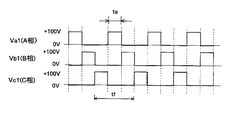
波形増幅器22a、22b、22cは、例えば図7に示すように各相の+100Vの印加時間taを繰り返し周期tfの1/3である約33%に設定した(これを「搬送電圧パターン」という。)、あるいは例えば図8又は図9に示すように、各相の+100V又は0Vの印加時間taを繰り返し周期tfの2/3である約67%に設定した(これを「ホッピング電圧パターン」という。)3相の駆動信号Va、Vb、Vcを出力する。
【0049】
そして、この波形増幅器22a、22b、22cからの駆動信号Va、Vb、Vcを、搬送基板1の駆動信号印加用入力端子16a、16b、16cを介してa相共通電極15a、b相共通電極15b、c相共通電極15cにそれぞれ印加する。
【0050】
ここで、搬送基板1の共通電極15a、15b、15c、すなわち搬送電極12a、12b、12cに例えば搬送電圧パターンの駆動信号Va、Vb、Vcを印加した場合、搬送基板1上の帯電粉体は搬送電極12a、12b、12cからの進行波電界を受けて所定の方向に搬送される。また、搬送基板1の共通電極15a、15b、15c、すなわち搬送電極12a、12b、12cに例えばホッピング電圧パターンの駆動信号Va、Vb、Vcを印加した場合、搬送基板1上の帯電粉体は搬送電極12a、12b、12cからの進行波電界を受けてホッピングしながら所定の方向に搬送される。
【0051】
本発明者らは、搬送電極12をL(幅)/S(電極間距離)=10/20μm、搬送電極12の長さ(搬送方向と直交する方向の長さ)60mmとして、ト−タル2700本の搬送電極12を形成した搬送基板1を上述したようにして作製した。この結果、顕微鏡観察で3μm〜10μm長さの断線が5本確認された。
【0052】
そこで、このサンプルの搬送基板1を用いて、帯電したトナーについての搬送実験を行い、3相の互いに位相がずれた駆動パルス電圧100V、駆動周波数3kHzの駆動信号Va、Vb、Vcを共通電極15a、15b、15cにそれぞれ印加した。
【0053】
この結果、従来トナ−搬送開始地点から最初の断線部分でトナ−溜まりの発生があったが、本サンプルにおいてはトナ−の溜まりが発生することなく、また、他の断線部分においても溜まりは観察されず、所定方向へトナが搬送されることが確認できた。なお、搬送速度は0.55m/secであった。
【0054】
このように、搬送基板には搬送電極の両端部にて相互接続される共通電極が形成されているので、搬送電極の両側から駆動信号を印加できるようになり、断線による粉体溜まりを低減することができて、粉体を確実に静電力で水平方向に安定して搬送することができるとともに、従来のように対向電極を用いないのでETH現像にも適用することができる。
【0055】
次に、本発明に係る静電搬送装置の第2実施形態について図10ないし図14を参照して説明する。なお、図10は同静電搬送装置の搬送基板の平面説明図、図11は図10のE−E線に沿う断面説明図、図12は図10のF−F線に沿う断面説明図、図13は図10のG−G線に沿う断面説明図、図14は図10のH−H線に沿う断面説明図である。
【0056】
本実施形態では、搬送基板1は、支持基板11上にa相、b相、c相共通電極15a、15b、15c及び駆動信号印加用入力端子16a、16b、16cをそれぞパターンニングして形成し、その表面に層間絶縁膜17を成膜し、この層間絶縁膜17に各搬送電極12a、12b、12c用のコンタクトホール18を形成し、層間絶縁膜17上に各搬送電極12a、12b、12cを形成してコンタクトホール18を介してa相、b相、c相共通電極15a、15b、15cにそれぞれ接続している。
【0057】
本実施形態の搬送基板1を第1実施形態と同様にして作製したところ、3本の断線が発生したが、上記実験条件と同条件で確認した結果、帯電トナ−は滞留することはなく移動し、搬送速度は0.50m/secであった。
【0058】
次に、本発明に係る静電搬送装置の第3実施形態について図15ないし図19を参照して説明する。なお、図15は同静電搬送装置の搬送基板の平面説明図、図16は図15のI−I線に沿う断面説明図、図17は図15のJ−J線に沿う断面説明図、図18は図15のK−K線に沿う断面説明図、図19は図15のL−L線に沿う断面説明図である。
【0059】
本実施形態では、搬送基板1は、支持基板11上にc相の共通電極15c及び搬送電極12c並びに駆動信号印加用入力端子16cを一体形成し、その表面に層間絶縁膜17aを成膜して、この層間絶縁膜17a上にb相共通電極15b及び搬送電極12b並びに駆動信号印加用入力端子16bを一体形成し、更にその表面に層間絶縁膜17bを成膜し、この層間絶縁膜17b上にa相共通電極15a及び搬送電極12a並びに駆動信号印加用入力端子16aを形成して、その表面に表面保護層13を成膜した後、駆動信号印加用入力端子16a、16b、16cに対応する部分をそれぞれエッチングで開口した。
【0060】
このように、ここでは各共通電極と各搬送電極を一体形成し、層間絶縁膜と、交互に積層する形態で形成している。この場合も前同様の実験によれば、断線が生じていてもトナーが滞留することなく移動することが確認できた。
【0061】
なお、上記各実施形態において、駆動信号(駆動電圧)を印加する入力端子を図に示す搬送電極と同方向の4端部に設けているので、いずれの入力端子も駆動電源(駆動回路)と接続でき、また、いずれか2カ所、もしくは4カ所すべてに接続することも可能となる。これによって、実装性が広く取れるとともにに駆動信号(駆動電圧)印加に対する信頼性が向上する。
【0062】
次に、本発明に係る静電搬送装置の第4実施形態について図20ないし図22を参照して説明する。なお、図20は同静電搬送装置の搬送基板の平面説明図、図21は図20のM−M線に沿う断面説明図、図22は図20のN−N線に沿う断面説明図である。
【0063】
本実施形態では、搬送基板1は、支持基板11の一方の面(裏面)にa相、b相、c相の各共通電極15a、15b、15c及び駆動信号印加用入力端子16a、16b、16cをそれぞれ形成して絶縁保護膜27で被覆し、支持基板11の他方の面(表面)にa相、b相、c相の各搬送電極12a、12b、12cをそれぞれ形成して表面保護層13で被覆している。
【0064】
そして、支持基板11に形成したスルーホール28を介して各搬送電極12a、12b、12cをそれぞれa相、b相、c相の各共通電極15a、15b、15cに接続している。
【0065】
このように支持基板11の裏面側にa相、b相、c相の各共通電極15a、15b、15cを配置することによって、搬送電極12a、12b、12c間での段差をなくし、また、搬送基板1全体の厚さを薄くすることができる。ただし、搬送基板自体にスルーホールを形成しなければならない点では、前記第1ないし第3実施形態よりも製造プロセス上は不利である。
【0066】
次に、本発明に係る静電搬送装置の第5実施形態について図23を参照して説明する。なお、同図は同静電搬送装置の搬送基板の平面説明図である。
本実施形態では、前記第1実施形態と同様な共通電極15及び搬送電極12の構成(相互接続形態を含む)とし、一端部側の共通電極15a、15b、15cには両端部に駆動信号印加用入力端子16a、16b、16cを設けたが、他端部側の共通電極15a、15b、15cには駆動信号印加用入力端子を設けない構成とした。
【0067】
この搬送基板1について前記第1実施形態と同様にしてサンプルを作製して、得られたサンプルについて搬送確認実験を行った。このとき、b相共通電極15bとc相共通電極間(上部より20本目)の搬送電極12bが断線していたが、トナ−が留まることなく移動することが確認できた。
【0068】
これは、搬送電極12の両端部に共通電極15を配置することにより断線以外の搬送電極12を通じて駆動信号(駆動電圧)が印加される効果である。従来、同様の現象においては、断線した搬送電極手前部分にトナ−が滞留するのが確認されたが、これは断線した搬送電極に駆動電圧が印加されないため搬送電極間が見かけじょう広くなり、進行波電界が及ばないためトナ−が堆積するためと思われる。
【0069】
なお、このような構成は、前記第2ないし第4実施形態の搬送基板にも同様に適用することができる。
【0070】
次に、本発明に係る静電搬送装置の第6実施形態について図24を参照して説明する。なお、同図は同静電搬送装置の搬送基板の平面説明図である。
本実施形態では、前記第1実施形態と同様な共通電極15及び搬送電極12の構成(相互接続形態を含む)とし、各端部側の共通電極15a、15b、15cから引出し部19a、19b、19cを一体形成して、粉体搬送方向と直交する方向で各端部側の共通電極15a、15b、15cよりも外側に駆動信号印加用入力端子16a、16b、16cを配置している。
【0071】
なお、このような構成は、前記第2ないし第5実施形態の搬送基板にも同様に適用することができる。
【0072】
次に、本発明に係る静電搬送装置の第7実施形態について図25を参照して説明する。なお、同図は同静電搬送装置の搬送基板の平面説明図である。
本実施形態は、粉体搬送のより効率性を図る目的から第1実施形態で実施した形態において、配線抵抗の低抵抗化を図り前記粉体の搬送効率を向上している。
【0073】
すなわち、本実施形態では、前記第1実施形態と同様な共通電極15及び搬送電極12の構成(相互接続形態を含む)とし、各端部側の共通電極15a、15b、15cを粉体搬送に影響を与えない領域で外部共通電極20a、20b、20で相互に接続した。
【0074】
この場合、外部共通電極20a、20b、20cの形成方法としては、搬送電極材料よりも抵抗率の低い材料を用いる、または、配線材料膜厚を厚く形成する、若しくは前記搬送電極と同材料でパタ−ン幅を広く取るなどの形態とすることができる。
【0075】
ここでは、プロセス工程を増やすことなく同一工程(搬送電極と共通電極を形成する工程)で形成することが可能なように、Alからなる搬送電極12に対し広い電極幅の外部共通電極を形成し、その後、スパッタにてSiO2の表面保護層を1μm厚みに成した。
【0076】
本実施形態のサンプルを作製して、球形トナ−を用いて搬送状況を確認した結果、所定方向にトナーが滞留することなく移動されるのを確認できた。搬送速度は駆動パルス電圧100V、駆動周波数3kHzで0.7m/secを確認した。また、駆動パルス電圧40V、駆動周波数3kHzの場合でも、0.55m/secが得られ、低駆動電圧で駆動することが確認できた。
【0077】
なお、本実施形態も前記第2ないし第6実施形態の構成に同様に適用することができる。
【0078】
次に、上述した各実施形態で用いている共通電極と搬送電極の相互接続について図26及び図27を参照して説明する。なお、図26は本発明に係る搬送基板のコンタクトホール部分の断面説明図、図27は従来のコンタクトホール部分の断面説明図である。
【0079】
相互接続においては、一体形成法とコンタクトホ−ルを介して共通電極と搬送電極を接続する方法がある。一体で形成する方法が配線上の信頼性は好ましいが、電極及び層間絶縁膜を薄層にした一層一電極を形成した場合用いることが可能となるが、厚膜においては電極間の段差凹凸が大きくなるとともに、工程数が増加することとなる。また、同じ駆動電圧の駆動信号であれば、最下部電極と最上部電極との段差による電界強度が異なるため、電極および層間膜の膜厚等の最適化が必要となる。このことは、総電極数が多い場合ますます重要課題となり得る。
【0080】
そこで、上記各実施形態においては、導体接合に従来より半導体形成技術等で用いられているコンタクトホ−ルを介して接合する形成法と先の一体形成を混在した方法の両者を適用している。
【0081】
このコンタクトホ−ルを形成するには、2通りの方法がある。一つは図27に示すように、支持基板11上に搬送電極12を形成し、この搬送電極12上に成膜された層間絶縁膜17にコンタクトホ−ル18を形成し、その後、共通電極15を形成する方法である。
【0082】
このように、搬送電極上にコンタクトホ−ルを形成するに当たっては、コンタクトホ−ル形成用マスクを用いて位置合わせをし、レジストパタ−ンを形成する。一般的なコンタクトホ−ルの形状としては、角型(正方形、長方形)形状が多いが、そのため孔の壁面が急峻に近い形で形成されコンタクトホ−ルの底部及び上部において後の共通電極となる電極材料(Al)を成膜し、共通電極を形成した際、前記底部及び前記上部においてボイド及びカバレ−ジ不良による断線を起こすおそれがある。
【0083】
また、コンタクトホ−ルの位置合わせ及びエッチングにおけるサイドエッチを注意する必要がある。これは、四方が同形状であるため等方的にエッチングされ急峻になるためである。コンタクトホ−ルの位置及びサイドエッチ量が大きいと搬送電極から孔が落ちた形で形成される。
【0084】
本実施例においては、幅(w)方向が10μmの搬送電極12上にコンタクトホ−ル18として8μmのホールを作製する場合、残り2μm(左右1μm)しか余裕がなく、万が一左右どちらかにレジストパタ−ンがずれ電極落ちした場合、後の共通電極との接合において接触面積が小さくなり、接触抵抗が高くなってしまう。
【0085】
そこで、図26に示すように、支持基板11上にまず共通電極15を形成した後、層間絶縁膜17にコンタクトホ−ル18を形成し、次に、搬送電極12を形成している。
【0086】
これにより、共通電極15の幅(本実施形態では500μmとしている。)が広いため、コンタクトホ−ル18の位置ずれ及びサイドエッチが多少大きくなった場合でも電極落ちすることがなくなる。
【0087】
さらに、本実施形態においては、接合の信頼性を向上させる狙いからコンタクトホ−ル18の形状を搬送電極12の方向に楕円形状に形成した。このように、Rを小さく採ることにより、コ−ナのエッチング速度が遅くなることを用いて壁面の傾斜をなだらかにし、段差及びボイドによる断線を防止することができる。なお、楕円のコンタクトホ−ルを用いたがこの形状に限られたものではなく、他の形状として、菱形、星形等を用いることもできる。
【0088】
次に、本発明に係る静電搬送装置を含む本発明に係る現像装置を含む本発明に係る画像形成装置の第1実施形態について図28を参照して説明する。なお、同図は同画像形成装置の全体概略構成図である。
この画像形成装置の全体の概略及び動作を説明すると、潜像担持体である感光体ドラム101(例えば、有機感光体:OPC)は同図で時計方向に回転駆動される。コンタクトガラス102上に原稿を載置し、図示しないプリントスタートスイッチを押すと、原稿照明光源103とミラー104とを含む走査光学系105と、ミラー106、107を含む走査光学系108とが移動して、原稿画像の読み取りが行われる。
【0089】
ここで、走査された原稿画像がレンズ109の後方に配置した画像読み取り素子110で画像信号として読み込まれ、読み込まれた画像信号はデジタル化され画像処理される。そして、この画像処理をした信号でレーザーダイオード(LD)を駆動し、このレーザーダイオードからのレーザー光をポリゴンミラー113で反射した後、ミラー114を介して感光体ドラム101上に照射する。この感光体ドラム101は帯電装置115によって一様に帯電されており、レーザー光による書き込みにより、感光体ドラム101の表面に静電潜像が形成される。
【0090】
そして、この感光体ドラム101表面の静電潜像は、本発明に係る静電搬送装置を含む本発明に係る現像装置116によってトナーが付着されて可視像化され、この可視像は、給紙部117A又は117Bから給紙コロ118A又は118Bで給紙された転写紙(記録媒体)119に転写チャージャ120のコロナ放電により転写される。この可視像が転写された転写紙119は、分離チャージャ121により感光体ドラム101の表面より分離されて、搬送ベルト122によって搬送され、定着ローラ対123の圧接部を通って、可視像が定着され、機外の排紙トレイ124へと排紙される。
【0091】
一方、転写が終了した感光体ドラム101の表面に残留しているトナーはクリーニング装置125によって除去され、感光体ドラム101の表面に残留している電荷は除電ランプ126によって消去される。
【0092】
次に、本発明に係る静電搬送装置を備えた本発明に係る現像装置116について図29を参照して説明する。なお、同図は同現像装置の概略構成図である。
この現像装置116は、粉体であるトナーを収納するトナーホッパ部131と、このトナーホッパ部131内のトナーを攪拌するアジテータ132と、トナーホッパ部131内のトナーを帯電させてトナーボックス部133に供給する帯電ローラ134及びこの帯電ローラ134の周面に接触させて配置したドクターブレード135と、トナーボックス部133内のトナーを静電力で搬送して潜像担持体である感光体ドラム101に向かってトナーを噴出させる本発明に係る静電搬送装置136と、現像に供されなかったトナーを回収するトナー回収部材138と、トナー回収部材138に回収されるトナーを静電力で搬送してトナーボックス部133に戻す本発明に係る静電搬送装置であるトナー逆搬送部材139とを備えている。
【0093】
静電搬送装置136は、先端部が感光体ドラム1近傍に臨み、帯電したトナーを静電力で搬送して先端部から感光体ドラム101に向かって噴出する搬送面14、14を有する2枚の搬送基板1、1を搬送面14、14を対向させて所定の間隔で配置している。
【0094】
そして、これらの搬送基板1、1間にトナーボックス部133内のトナーを静電力で搬送して送り込む送り込み基板143、143とを備え、これらの送り込み基板143、143の一端部は搬送基板141、141に接合し、他端部は帯電ローラ134側に配置している。なお、送り込み基板143も搬送基板1と同様な構成(ただし、支持基板にはポリイミドフィルムなどの変形可能な支持基板を用いている。)として、静電力で帯電したトナーを搬送基板1に搬送(ホッピングを伴なっても構わない。)する搬送基板としている。
【0095】
また、搬送基板1、1の複数の搬送電極12に対して駆動信号Va、Vb、cを印加する駆動回路150a、150bを備えている。この駆動回路150a、150bからの駆動信号Va、Vb、Vcは、前述したように搬送基板1、1の各共通電極15a、15b、15cを介して複数の各搬送電極12a、12b、12cに印加される。
【0096】
なお、接続関係の図示を省略しているが、この駆動回路150a、150bからの駆動信号Va、Vb、Vdは送り込み基板143の各搬送電極にも印加される。また、ここでは、各搬送基板1、1毎に駆動回路150a、150bを設けているが、1つの駆動回路を共用してもよい。ただし、各搬送基板毎に駆動回路を設ければ、つまり、異なる駆動信号を印加できるようにすれば、対向する搬送電極間の駆動信号の位相を異ならせることができる。
【0097】
このように構成した画像形成装置においては、図30に示すように、現像装置116のトナーホッパ部131のトナーがアジテータ132で攪拌されながら帯電ローラ134に運ばれ、帯電ローラ134の回転(図で左回り方向)によってドクタブレード135との摩擦帯電で所定の極性に帯電されてトナーボックス部133に送り込まれる。
【0098】
そして、このトナーボックス部133のトナーは、送り込み基板143、143に3相の駆動信号Va、Vb、Vcが印加されることで送り込み基板143に沿って搬送されて搬送基板1、1間に送り込まれ、搬送基板1に3相の駆動信号Va、Vb、Vcが印加されることで、搬送基板1に沿って多くの搬送量でスムーズに搬送されて、感光体ドラム101との対向部方向に向けて噴出側から順次供給される。
【0099】
これによって、噴出された帯電トナーは感光体ドラム101表面の逆極性電荷がある部分(画像部分)に付着して感光体ドラム101上の潜像が現像される。このとき、搬送基板1によるトナー搬送が効率的に確実に行われることから、現像に必要とされる十分なトナー量の供給を確保することができる。
【0100】
この場合、搬送基板1、1の先端部電極152、152間に交流電源153からの交流電圧を印加して交流電界を発生させておくと、搬送基板1、1間から噴出したトナーが交流電界によってクラウド状態になるトナークラウド154が発生し、感光体ドラム101の潜像に対して均質にトナーが付着するので、画像品質が向上する。
【0101】
次に、本発明に係る静電搬送装置を含む本発明に係る現像装置を備えた本発明に係る画像形成装置の第2実施形態について図31及び図32を参照して説明する。なお、図31は同画像形成装置の現像装置部分の概略構成図、図32は同現像装置の要部詳細説明図である。
【0102】
この画像形成装置の現像装置116は、ETH現像を行うための搬送基板1を含む静電搬送装置136を備えている。すなわち、ここでは、搬送基板1は、トナー送り込み基板143から供給されるトナーを現像部側に向かって搬送するためのトナー搬送部1T及びこのトナー搬送部1Tで搬送されるトナーを感光体ドラム101の近傍でホッピングさせるための現像部を構成しているトナーホッピング部1Pを一体に連続的に形成したものである。
【0103】
また、搬送基板1の複数の電極12に対して駆動信号Va、Vb、Vdを印加する駆動回路162を備えている。さらに、搬送基板1のトナーホッピング部1Pと感光体ドラム101との間に現像バイアス電圧であるDCバイアス(100V〜200V)を印加するための電極163及びDC電源164を備える構成も可能である。
【0104】
ここで、搬送基板1のトナー搬送部1Tはトナーを現像部であるトナーホッピング部1P側に向かって搬送する部分であって、粉体を潜像担持体側に向かって静電力で搬送する静電搬送装置を構成し、トナーホッピング部1Pはトナーを感光体ドラム101近傍で静電力でホッピングさせる部分であって、現像部を構成するものであって、粉体を潜像担持体近傍で静電力でホッピングさせるための静電搬送装置を構成している。
【0105】
なお、ここでは、搬送基板1のトナー搬送部1T及びトナーホッピング部1Pの電極構成、印加する駆動信号を同じにしているため、搬送基板1上のトナーはトナー搬送部1Tにおいてもトナーホッピング部1Pにおいても搬送及びホッピングが行われている。すなわち、「トナー搬送部」はトナーを現像部に搬送する目的を有する部分であるという意味で、また「トナーホッピング部」はトナーをホッピングする目的を有する部分であるという意味で使用しており、トナー搬送部ではホッピングが行われない、トナーホッピング部ではトナー搬送が行われないという意味ではない。
【0106】
この搬送基板1は、前述した本発明に係る静電搬送装置で説明したように、支持基板11上に進行波電界を発生させるための複数の電極12を設け、電極12の表面を表面保護層13で被覆したものである。そして、駆動回路162からの駆動信号Va、Vb、Vcは、前述したように搬送基板1の共通電極15a、15b、15cを介して各搬送電極12a、12b、12cに印加される。
【0107】
このように構成したこの画像形成装置における現像動作について説明すると、トナーボックス部33内の帯電したトナーは、トナー送り込み基板143によって静電力で搬送されて搬送基板1のトナー搬送部1Tに至り、このトナー搬送部1Tで更に静電力で感光体ドラム101側に向かって搬送されてトナーホッピング部1Pに送られる。
【0108】
そして、このトナーホッピング部1Pにおいては、図33に示すようにトナーTがホッピングしている。このように感光体ドラム101の近傍でトナーがホッピングしていることにより、感光体ドラム101の潜像部だけにトナーを付着させるためには、次のような電界を発生させればよい。すなわち、トナーホッピング部1Pの搬送電極12に印加するパルス状駆動電圧の平均値と感光体ドラム101に形成された潜像部電圧による電界は、トナーを感光体ドラム101側に吸引する関係、またトナーホッポング1Pの搬送電極12に印加するパルス状駆動電圧の平均値と感光体ドラム101に形成された非潜像部電圧による電界は、トナーを感光体ドラム101側から反発する方向関係に設定する。
【0109】
このとき、既にホッピングしているトナーは搬送基板1との間で吸着力が生じていないため、容易に潜像担持体(感光体ドラム101)側に移送することができ、高い画像品質が得られる現像を低電圧で行うことができる。
【0110】
すなわち、従来の所謂ジャンピング現像方式にあっては、現像ローラから帯電トナーを剥離させて感光体に移送させるには、トナーの現像ローラに対する付着力以上の印加電圧が必要であり、DC600〜900Vのバイアス電圧をかけなければならない。これに対して、本発明によれば、トナーの付着力は通常50〜200nNであるが、搬送基板1上でホッピングしているために搬送基板1に対する付着力が略零になるので、トナーを搬送基板1から剥離する力が不要になり、低電圧で十分にトナーを感光体側に移送することが可能になるのである。
【0111】
そして、トナーホッピング部1Pに送り込まれたが使用されないトナーは、トナーホッピング部1Pにおいてもホッピングとともに搬送が行われているので、トナー回収部材138に排出されて回収される。
【0112】
次に、本発明に係るプロセスカートリッジを備えた画像形成装置の第3実施形態について図34及び図35を参照して簡単に説明する。なお、図34は同画像形成装置の概略構成図、図35は同画像形成装置を構成するプロセスカートリッジの概略構成図である。
【0113】
この画像形成装置200は、マゼンダ(M)、シアン(C)、イエロー(Y)、ブラック(Bk)の4色でフルカラー画像を形成するレーザプリンタの一例であり、各色用の画像信号に応じたレーザビームを出射する4つの光書き込み装置201M、201C、201Y、201Bk(以下「光書き込み装置201」とも総称する。)と、作像用の4つのプロセスカートリッジ202M、202C、202Y、202Bkと、画像が転写される記録用紙を収納する給紙カセット203と、給紙カセット203から記録用紙を給紙する給紙ローラ204と、記録用紙を所定のタイミングで搬送するレジストローラ205と、記録用紙を各プロセスカートリッジの転写部に搬送する転写ベルト206と、記録用紙に転写された画像を定着する定着装置209と、定着後の記録用紙を排紙トレイ211に排紙する排紙ローラ210等を備えた構成となっている。
【0114】
4つのプロセスカートリッジ202M、202C、202Y、202Bkの構成は同じ(以下「プロセスカートリッジ202」とも総称する。)であり、図35に示すように、各プロセスカートリッジ202は、ケース内に像担持体であるドラム状の感光体221と、帯電ローラ222と、本発明に係る静電搬送装置を含む現像装置223と、クリーニングブレード224等を一体に備え、画像形成装置本体に対して着脱可能に構成している。現像装置223を着脱自在であるプロセスカ−トリッジ202内に具備させることにより、メンテナンス性の向上、他の装置との一体交換を容易に行うことができるようになる。
【0115】
また、現像装置223内には、トナー供給ローラ225、帯電ローラ226、本発明に係る静電搬送装置を構成する搬送基板1、搬送基板1へのトナー送り込み基板227、回収トナーを戻すトナー戻しローラ228が設けられており、各色のトナーが収納されている。また、プロセスカートリッジ202の背面側には、光書き込み装置201からのレーザビームが入射される窓口となるスリット230が設けられている。
【0116】
各光書き込み装置201M、201C、201Y、201Bkは、半導体レーザ、コリメートレンズ、ポリゴンミラー等の光偏向器、走査結像用光学系等から構成され、装置外部のパーソナルコンピュータ等のホスト(画像処理装置)から入力される各色用の画像データに応じて変調されたレーザビームを出射し、各プロセスカートリッジ202M、202C、202Y、202Bkの感光体221上を走査し、静電荷像(静電潜像)を書き込む。
【0117】
そして、画像形成が開始されると、各プロセスカートリッジ202M、202C、202Y、202Bkの感光体221が帯電ローラ222で均一に帯電され、各光書き込み装置201M、201C、201Y、201Bkから画像データに応じたレーザビームが照射されて各感光体上に各色の静電潜像が形成される。
【0118】
この感光体221上に形成された静電潜像は、現像装置223の搬送基板1によるETH現像により、各色のトナーによって現像され顕像化される。また、現像に供されなかったトナーは搬送基板1で搬送されてトナー戻しローラ228によってトナー送り込み基板227の入口側に戻される。このように、本発明に係る静電搬送装置を含む現像装置によって現像を行うことで、前述したように高品質の画像を形成することができる。
【0119】
一方、各プロセスカートリッジ202Bk、202Y、202C、202Mの各色の画像形成に同期して、供給カセット203内の記録用紙が供給ローラ204で給紙され、レジストローラ205により所定のタイミングで転写ベルト206に向けて搬送される。そして、記録用紙は転写ベルト206に担持されて4つのプロセスカートリッジ202Bk、202Y、202C、202Mの感光体221に向けて順次搬送され、各感光体上のBk、Y、C、Mの各色のトナー像が順次重ね合わせて転写される。4色のトナー像が転写された記録用紙は、定着ベルト207と加圧ローラ208からなる定着装置209に搬送され、4色のトナー像からなるカラー画像が定着されて排紙トレイ211に排紙される。
【0120】
次に、本発明に係るプロセスカートリッジを含む本発明に係る画像形成装置の第4実施形態について図36及び図37を参照して簡単に説明する。なお、図36は同画像形成装置の概略構成図、図37は同画像形成装置を構成するプロセスカートリッジの概略構成図である。
【0121】
この画像形成装置は、水平に延在する転写ベルト(像担持体)251に沿って、各色のプロセスカ−トリッジ260Y、260M、260C、260Bk(以下「プロセスカートリッジ260」とも総称する。)を並置したタンデム方式のカラー画像形成装置である。なお、プロセスカ−トリッジ260は、イエロー、マゼンタ、シアン、ブラックの順で説明したが、この順番に特定されるものではなく、どの順番で並置してもよい。
【0122】
プロセスカ−トリッジ260は、像担持体261、帯電手段262、本発明に係る静電搬送装置の搬送基板1を含む現像手段263、クリーニング装置264等の構成要素のうち、複数のものをプロセスカ−トリッジとして一体に結合して構成し、このプロセスカ−トリッジを複写機やプリンタ等の画像形成装置本体に対して着脱可能に構成している。
【0123】
通常、カラーの画像形成装置は複数の画像形成部を有するため装置が大きくなってしまう。また、現像装置、クリーニングや帯電などの各ユニットが個別で故障したり、寿命による交換時期がきた場合は、装置が複雑でユニットの交換に非常に手間がかかっていた。
【0124】
そこで、少なくとも像担持体と現像手段の構成要素をプロセスカ−トリッジ260として一体に結合して構成することによって、ユーザーによる交換も可能な小型で高耐久のカラー画像形成装置を提供することができる。
【0125】
ここで、各色のプロセスカ−トリッジ260Y、260M、260C、260Bkで現像された像担持体262上の現像トナーは水平に延在する転写電圧が印加された転写ベルト251に順次転写される。
【0126】
このようにイエロー、マゼンタ、シアン、ブラックと画像の形成が行なわれ、転写ベルト251上に多重に転写され、転写手段252で転写材253にまとめて転写される。そして、転写材253上の多重トナー像は図示しない定着装置によって定着される。
【0127】
上記各実施形態で説明した画像形成装置は、いずれも本発明に係る静電搬送装置を含む現像手段(装置)を備えているので、装置の小型化、低コスト化を図れ、トナ−飛散などもなく、画像品質を向上することができる。
【0128】
なお、上記実施形態においては、粉体としてトナーを例に説明しているが、トナー以外の粉体を搬送するための装置などにも同様に適用することができる。また、搬送電極に印加する駆動信号は3相を例に説明しているが、4相、6相などでもよい。
【0129】
【発明の効果】
以上説明したように、本発明に係る静電搬送装置によれば、搬送基板には搬送電極の両端部側に相互接続される共通電極が形成されている構成としたので、搬送電極の断線等が生じても粉体溜まりの発生を低減して、簡単な構成で粉体を安定して移動させることができるとともに、ETH現像にも適用することができるようなる。
【0130】
本発明に係る現像装置によれば、帯電トナーを移動させる本発明に係る静電搬送装置の搬送基板を備えているので、小型で、安定した高品質現像を行うことできる。
【0131】
本発明に係るプロセスカートリッジによれば、本発明に係る現像装置を含む構成としたので、小型で、安定した高品質現像を行うことできるプロセスカートリッジが得られる。
【0132】
本発明に係る画像形成装置によれば、本発明に係る現像装置を備え、或いはプロセスカートリッジを複数備えているので、高品質現像を行うことができて高品質画像を形成できる。
【図面の簡単な説明】
【図1】本発明に係る静電搬送装置の第1実施形態の搬送基板の平面説明図
【図2】図1のA−A線に沿う断面説明図
【図3】図1のB−B線に沿う断面説明図
【図4】図1のC−C線に沿う断面説明図
【図5】図1のD−D線に沿う断面説明図
【図6】同搬送基板に対して駆動信号を印加する駆動回路の一例を説明するブロック図
【図7】同駆動信号の一例を説明する説明図
【図8】同駆動信号の他の例を説明する説明図
【図9】同駆動信号の更に他の例を説明する説明図
【図10】本発明に係る静電搬送装置の第2実施形態の搬送基板の平面説明図
【図11】図10のE−E線に沿う断面説明図
【図12】図10のF−F線に沿う断面説明図
【図13】図10のG−G線に沿う断面説明図
【図14】図10のH−H線に沿う断面説明図
【図15】本発明に係る静電搬送装置の第3実施形態の搬送基板の平面説明図
【図16】図15のI−I線に沿う断面説明図
【図17】図15のJ−J線に沿う断面説明図
【図18】図15のK−K線に沿う断面説明図
【図19】図15のL−L線に沿う断面説明図
【図20】本発明に係る静電搬送装置の第4実施形態の搬送基板の平面説明図
【図21】図20のM−M線に沿う断面説明図
【図22】図20のN−N線に沿う断面説明図
【図23】本発明に係る静電搬送装置の第5実施形態の搬送基板の平面説明図
【図24】本発明に係る静電搬送装置の第6実施形態の搬送基板の平面説明図
【図25】本発明に係る静電搬送装置の第7実施形態の搬送基板の平面説明図
【図26】本発明に係る静電搬送装置の各実施形態の搬送基板におけるコンタクトホールによる相互接続の説明に供する断面説明図
【図27】比較例のコンタクトホールによる相互接続の説明に供する断面説明図
【図28】本発明に係る画像形成装置の第1実施形態の説明に供する概略構成図
【図29】同画像形成装置の本発明に係る現像装置の説明に供する概略構成図
【図30】同画像形成装置の現像作用の説明に供する説明図
【図31】本発明に係る画像形成装置の第2実施形態の説明に供する概略構成図
【図32】同画像形成装置の本発明に係る現像装置の説明に供する概略構成図
【図33】同画像形成装置の現像作用の説明に供する説明図
【図34】本発明に係る画像形成装置の第3実施形態の説明に供する概略構成図
【図35】同画像形成装置の本発明に係るプロセスカートリッジの説明図
【図36】本発明に係る画像形成装置の第4実施形態の説明に供する概略構成図
【図37】同画像形成装置の本発明に係るプロセスカートリッジの説明図
【図38】一般的な静電搬送装置の搬送基板の平面説明図
【図39】同搬送装置の構成を説明する構成図
【図40】同搬送装置によるトナー搬送不良の発生を説明する説明図
【符号の説明】
1…搬送基板、11…支持基板、12a、12b、12c…電極、13…表面保護層、14…搬送面、15a、15b、15c…共通電極、16a、16b、16c…駆動信号印加用入力端子、20a、20b、20c…外部共通電極、101…感光体ドラム(潜像担持体)、116…現像装置、136…静電搬送装置、202、260…プロセスカートリッジ。[0001]
[Industrial applications]
The present invention relates to an electrostatic transport device, a developing device, a process cartridge, and an image forming device.
[0002]
[Patent Document 1] Japanese Patent Application Laid-Open No. 2001-139144
[Patent Document 2] JP-A-2002-341656
[Prior art]
2. Description of the Related Art As an image forming apparatus such as a copying apparatus, a printer, and a facsimile, a latent image is formed on a latent image carrier using an electrophotographic process, and a developer (hereinafter, also referred to as “toner”) is formed on the latent image. There is a type in which an image is formed by attaching and developing a toner image into a visible image as a toner image and transferring the toner image to a recording medium (including an intermediate transfer member).
[0003]
In such an image forming apparatus, as a toner conveying apparatus for conveying the toner, an apparatus using a rotatable screw is generally used. For example, it is known that toner in a pipe is conveyed in the axial direction of the screw by rotating a screw provided along the inside of the pipe.
[0004]
However, in such a toner conveying device, a relatively large motor is used to rotate the screw in the pipe, so that there is a problem that the device area becomes large and the rotating noise is large. Further, when toner is clogged between the inner wall of the pipe and the screw, the toner is melted by frictional heat, which may cause an increase in torque or poor conveyance.
[0005]
On the other hand, other toner conveying devices include a device that conveys the toner together with the airflow by applying or entraining the airflow on the toner, a device that conveys the toner by helping the toner to slide down along the slope due to vibration, a device that conveys the toner, There are also known devices for transporting an image by an electric field.
[0006]
Among these, in an apparatus that transports the toner together with the air flow, the transport density of the minute particulate matter is reduced by air and becomes sparse, and this is a low-efficiency transport method. Further, in a device that transports toner that assists transportation by vibration, relatively large energy is required to cause the vibration, and there is a disadvantage that the transportation direction is limited to the direction of gravity.
[0007]
Therefore, the apparatus for transporting the charged toner using the above-described electric field does not involve abrasion or vibration of the mechanical part, so that it is possible to maintain a long-term stable image forming operation without noise. Transport equipment
[Patent Document 1]
It is disclosed in Patent Document 2 and the like.
[0008]
A general toner conveying device using this electric field will be described with reference to FIGS. FIG. 38 is an explanatory plan view of the toner conveying device, and FIG. 39 is an explanatory sectional view of the conveying electrode portion.
[0009]
In this toner transport device, a large number of transport electrodes 502 made of a thin film having a predetermined electrode width are arranged at predetermined electrode intervals on a support substrate 501 made of an insulator, and an insulating film 503 for preventing short circuit is provided on the surface thereof. Are formed to cover the transport electrode 502 and configure the transport substrate 500 with the surface of the insulating film 503 as the transport surface 504. The power supply electrodes 505a, 505b, and 505c are provided on the support substrate 501 on one end side of the transport electrodes 502. In addition,
In Patent Document 1, each of the power supply electrodes 505a, 505b, and 505c and the transport electrode 502 have a structure in which they are laminated with an insulating film interposed therebetween.
[0010]
Here, for example, three-phase driving voltages (driving signals) va, vb, vc which are shifted in phase from each other are supplied to the transport electrode 502 via the feeding electrodes 505a, 505b, 505c to generate a traveling wave electric field. Thus, the charged toner can be transported in the direction of the arrow in FIG. 38 by the action of the electric field.
[0011]
In such a toner transport device, in order to accurately transport the toner by the electric field, the toner movement control must be performed such that the toner is separated from one electrode and stopped on the other electrode. In addition, the above-described movement control must be performed on all the electrodes.
[0012]
By the way, on the carrier substrate, a large number of linear carrier electrodes having a width of about 0.01 to 1 mm are formed at intervals of about 0.01 to 1 mm and arranged in a row in a comb shape using photolithography technology. In this case, the electrode width needs to be matched with the particle size from the viewpoint of control by the electric field with respect to the toner, and the width is preferably narrow from the viewpoint of low voltage driving.
[0013]
However, in the case where thousands of narrow transport electrodes are formed in the electrode formation, no matter how the electrodes are formed in a clean room environment, it is difficult to select no defect, and defects such as disconnection may occur. . When a part of such a transport electrode is disconnected, for example, as shown in FIG. 40, when a disconnection 510 occurs in the middle of one transport electrode 502, a voltage is applied to a portion beyond the location of the disconnection 510. Cannot be supplied, and no electric field is generated in a portion ahead of the transport electrode 502. Therefore, the toner stops at the transport electrode immediately before the disconnection of the toner, and a toner pool 511 is generated. The toner is no longer conveyed.
[0014]
Further, in a conventional toner conveying device using an electric field, if there are relatively coarse particles agglomerated in the toner to be conveyed, the contact area with the conveyance substrate increases, and the traveling wave electric field for these particles increases. The transportability is poor, and the machine stops at the defective portion.
[0015]
When the toner stops on the transfer board in this way, the stopped toner blocks the transfer path and hinders the transfer of other toner, so that the transferability is deteriorated and the transfer failure occurs. And it becomes difficult to obtain good visualization.
[0016]
In this case, as a means for preventing the transfer failure of the charged toner, it is conceivable to increase the signal voltage applied to each transfer electrode and increase the intensity of the generated electric field to increase the transfer force. It is necessary to consider higher dielectric strength between the electrodes.
[0017]
Therefore,
In the transfer device described in Patent Literature 1, a counter electrode is disposed to face the transfer electrode with a gap therebetween, and an alternating electric field is generated between the transfer electrode and the counter electrode, and the transfer device is charged by the alternating electric field. By causing the toner to fly between the transport electrode and the counter electrode, the toner is transported in the transport direction by a traveling wave electric field generated between the transport electrodes.
[0018]
[Problems to be solved by the invention]
However, as mentioned above
As described in Patent Document 1, in order to generate an alternating electric field with a counter electrode facing a transfer electrode of a transfer substrate at a predetermined interval, the transfer electrode is driven to transfer the charged toner. In addition to the transport input power supply for inputting a voltage, a power supply for generating an alternating electric field for causing charged toner to fly between the transport electrode and the counter electrode must be provided, which complicates the configuration.
[0019]
Also, as described above, when the transport electrode is disconnected in the longitudinal direction, the voltage is supplied to the connection side with the transport input power supply, but the voltage is not supplied to the portion beyond the disconnection point, so that the toner Therefore, even if an alternating electric field generated by the counter electrode is used, the transportability is poor as in the above, and the defective portion stays at the defective portion.
[0020]
Further, in such a configuration using the counter electrode, the applicant has
It cannot be applied to ETH development as disclosed in Patent Document 2. The ETH (Electrostatic Transport & Hopping) phenomenon refers to a phenomenon in which powder is given the energy of a phase-shift electric field, the energy is converted into mechanical energy, and the powder itself fluctuates dynamically. . The ETH phenomenon includes a movement (conveyance) of powder in a horizontal direction (meaning a direction along a conveying surface) and a movement (hopping) in a vertical direction (meaning a vertical direction of a conveying surface) due to electrostatic force. This is a phenomenon in which the powder jumps on the surface of the electrotransport substrate with a component in the traveling direction due to the phase-shift electric field. Development utilizing this ETH phenomenon is referred to as ETH development.
[0021]
Therefore, the present inventors
In addition to the conventional electrostatic transport device that presupposes the horizontal transport of toner as described in Patent Document 1, a solution that can be applied to an electrostatic transport device applicable to ETH development will be found. As a result of intensive studies, the present invention has been accomplished, and an electrostatic transport device capable of stably moving powder with a simple configuration, a developing device using the electrostatic transport device, and a process cartridge And an image forming apparatus.
[0022]
In order to solve the above problems, in the electrostatic transport device according to the present invention, the transport electrodes for generating electrostatic force for moving the powder on the support substrate are substantially parallel to the moving direction at predetermined intervals and substantially orthogonal to the moving direction. A transfer substrate that is repeatedly formed and arranged in the direction, and further has a transfer surface formed of an insulating member on the surface, and a common electrode interconnected at both ends of the transfer electrode is formed on the transfer substrate. Configuration. In this specification, the term “powder” is used to include “particles”, “fine particles”, “powder”, “fine powder”, “powder”, “fine powder”, and the like.
[0023]
Here, it is preferable that an input terminal for applying an n-phase (n is an integer of 3 or more) drive signal application terminal is provided on the common electrode interconnected at both ends of the transport electrode. A drive signal application input terminal may be provided on one side of the common electrode on both sides to be connected, and the drive signal application input terminal may not be provided on the other side. In addition, the drive signal application input terminal may be arranged at a position extended outside the common electrode in a direction orthogonal to the moving direction.
[0024]
In addition, the n-phase common electrode and the transport electrode connected to each common electrode are in different layers, or the common electrode and the transport electrode connected to this common electrode are at least two of the n-phases. The phases can be arranged in the same layer for each phase.
[0025]
Further, the common electrodes on both sides may be connected to each other in a low-resistance pattern other than the transport electrodes. Further, it is preferable that the common electrode has a wider electrode width than the transport electrode.
[0026]
Furthermore, a common electrode interconnected by integral formation and a carrier electrode connected to the common electrode, or a common electrode interconnected via a contact hole and a carrier electrode connected to the common electrode May be included. In the case of interconnection using this contact hole, it is preferable that the common electrode and the transport electrode are stacked in this order from the surface of the support substrate.
[0027]
Further, the common electrode and the transport electrode can be provided on different surface sides of the support substrate. Further, at least two transfer substrates having transfer surfaces opposed to each other can be provided.
[0028]
The developing device according to the present invention is configured to include the transport substrate of the electrostatic transport device according to the present invention for moving the charged toner.
[0029]
The process cartridge according to the present invention has a configuration including the developing device according to the present invention.
[0030]
An image forming apparatus according to the present invention includes the developing device according to the present invention, or includes a plurality of process cartridges.
[0031]
BEST MODE FOR CARRYING OUT THE INVENTION
Hereinafter, embodiments of the present invention will be described with reference to the accompanying drawings. First, a first embodiment of the electrostatic transport device according to the present invention will be described with reference to FIGS. 1 is a plan view of a transfer substrate of the electrostatic transfer device, FIG. 2 is a cross-sectional view taken along line AA of FIG. 1, FIG. 3 is a cross-sectional view taken along line BB of FIG. FIG. 4 is a cross-sectional explanatory view along the line CC of FIG. 1, and FIG. 5 is a cross-sectional explanatory view along the line DD of FIG.
[0032]
The electrostatic transport device has a transport substrate 1 having a plurality of electrodes for generating an electric field for transporting and hopping toner as a powder. The transport substrate 1 has an n-phase (n) Are integers of 3 or more), the drive signals Va (a phase), Vb (b phase), and Vc (c phase) are input. Note that, here, the ETH current
I will explain with the transfer board that generates the elephant, but
As disclosed in Patent Document 1, the present invention can be similarly applied to a transfer substrate that moves powder only in a horizontal direction.
[0033]
The transfer substrate 1 has a set of three electrodes (transfer electrodes) 12a, 12b, and 12c (collectively referred to as “transfer electrodes 12”) on a base substrate (support substrate) 11 at a predetermined interval. In the powder moving direction is repeatedly formed and arranged in a direction substantially orthogonal to the powder moving direction, further forming a surface protection layer 13 made of an insulating member formed of an inorganic or organic insulating material on the surface thereof, The surface of the surface protection layer 13 is a transfer surface 14. In this case, the surface protective layer 13 is a surface layer forming the transport surface 14, but a surface layer having more excellent compatibility with powder can be separately formed on the surface protective layer 13.
[0034]
On both sides of the transport electrodes 12a, 12b and 12c, common electrodes 15a, 15b and 15c interconnected at both ends with the transport electrodes 12a, 12b and 12c, respectively (these are collectively referred to as "common electrodes 15"). ) Are provided along the powder moving direction, that is, in a direction substantially orthogonal to the individual transport electrodes. In this case, the width of the common electrode 15 (this width is a width in a direction orthogonal to the powder moving direction) is larger than the width of the transport electrode 12 (the width is a width in the direction along the powder moving direction). I have.
[0035]
Further, drive signal application input terminals 16a, 16b, and 16c for inputting drive signals Va, Vb, and Vc, respectively, are provided at both ends of the common electrodes 15a, 15b, and 15c (these are referred to as "drive signal application input terminals"). 16 ").
[0036]
Here, as the support substrate 11, a substrate made of an insulating material such as a glass substrate, a resin substrate or a ceramics substrate, or a substrate made of a conductive material such as SUS is used. 2 And a substrate made of a flexible and deformable material such as a polyimide film.
[0037]
In addition, as an electrode material of the transport electrode 12 and the common electrode 15, a conductive material such as Al, Ni—Cr, or the like can be used. The conductive material is patterned into a required electrode shape using a photolithography technique or the like. I have. In addition, the width of the transport electrode 12 in the powder advancing direction is set to be 1 to 20 times the average particle diameter of the powder to be moved, and the distance between the transport electrodes 12 and 12 in the powder advancing direction is also smaller. The average particle size is at least 1 and at most 20 times.
[0038]
As the surface layer 13, for example, SiO 2 , TiO 2 , TiO 4 , SiON, BN, TiN, Ta 2 O 5 Etc. can be used. Further, an inorganic nitride compound, for example, SiN, Bn, W, or the like can be used. In particular, when the number of surface hydroxyl groups increases, the charge amount of the charged powder tends to decrease during transportation. Therefore, an inorganic nitride compound having a small number of surface hydroxyl groups (SiOH, silatol groups) is preferable.
[0039]
Also, here, the a-phase and b-phase transport electrodes 12a, 12b and the common electrodes 15a, 15b are interconnected via contact holes, and the c-phase transport electrode 12c and the common electrode 15c are integrally formed. To form an interconnected structure in which the integrated formation and the interconnection by the contact hole are mixed.
[0040]
Therefore, in the transport electrode 1, the common electrodes 15a, 15b, 15c and the transport electrode 12c are formed in the same layer position, and the interlayer insulating film 17 (surface) on the surface of the common electrodes 15a, 15b, 15c and the transport electrode 12c is formed. The transport electrodes 12a and 12b are formed at the same layer position via the same insulating material as the protective layer 13 or a different material.
[0041]
In order to manufacture such a transfer substrate 1, for example, a Ni—Cr film is formed as an electrode material on a support substrate 11 using an insulating substrate such as glass, and the c-phase common electrode 15 c and the transfer electrode 12 c are integrated. At the same time as the formation and patterning, the a-phase common electrode 15a and the b-phase common electrode 15c are etched and patterned with a cerium nitrate solution (Ce) in the same step. At this time, the drive signal application input terminals 16a, 16b, and 16c of the common electrodes 15a, 15b, and 15c are simultaneously patterned.
[0042]
Then, an interlayer insulating film (here, SiO 2 Was used. ) 17 is formed on the entire surface in a thickness of 2 μm.
[0043]
Thereafter, a contact hole 18 is formed in the interlayer insulating film 17 using buffered hydrofluoric acid (BHF) at a connection position for interconnecting the a-phase common electrode 15a, the b-phase common electrode 15b and the transport electrodes 12a, 12b, respectively. I do.
[0044]
Subsequently, after Al for forming the transport electrodes 12a and 12b is formed on the surface of the interlayer insulating film 17, it is etched and patterned into an electrode shape with a phosphoric acid-based etchant, and the a-phase common electrode 15a and the b-phase common electrode are formed. The transport electrodes 12a and 12b interconnected via the contact holes 18 are formed on the electrodes 15b.
[0045]
Further, a surface protective layer 13 is formed on the surface. The drive signal application input terminals 16a, 16b, and 16c are formed except for the drive signal application input terminals 16a, 16b, and 16c when the interlayer insulating film 17 and the surface protection layer 13 are formed. Alternatively, the surface protection layer 13 and the interlayer insulating film 17 may be opened by etching.
[0046]
Next, an example of a drive circuit that supplies a drive signal to the transport substrate 1 configured as described above will be described with reference to FIG.
This drive circuit includes a pulse signal generation circuit 21 that generates and outputs a pulse signal, and waveform amplifiers 22a, 22b, and 22c that receive pulse signals from the pulse signal generation circuit 21 to generate and output drive waveforms Va, Vb, and Vc. And
[0047]
The pulse signal generating circuit 21 receives, for example, an input pulse of a logic level, and performs a phase shift by 120 ° on each pulse. The pulse signal generating circuit 21 drives a switching unit included in the next-stage waveform amplifiers 22a to 22c, for example, a transistor to switch 100V. And generates and outputs a pulse signal having an output voltage of 10 to 15 V at a level capable of performing the above operation.
[0048]
In the waveform amplifiers 22a, 22b, and 22c, for example, as shown in FIG. 7, the +100 V application time ta of each phase is set to about 33%, which is 1 / of the repetition period tf (this is referred to as a “carrier voltage pattern”). 8 or 9, for example, the application time ta of +100 V or 0 V for each phase is set to about 67%, which is 2/3 of the repetition period tf (this is referred to as a "hopping voltage pattern"). 3) Output three-phase drive signals Va, Vb, and Vc.
[0049]
The drive signals Va, Vb, and Vc from the waveform amplifiers 22a, 22b, and 22c are applied to the a-phase common electrode 15a and the b-phase common electrode 15b via the drive signal application input terminals 16a, 16b, and 16c of the carrier substrate 1. , C-phase common electrode 15c.
[0050]
Here, for example, when drive signals Va, Vb, Vc of a carrier voltage pattern are applied to the common electrodes 15a, 15b, 15c of the carrier substrate 1, that is, the carrier electrodes 12a, 12b, 12c, the charged powder on the carrier substrate 1 Receiving the traveling wave electric field from the transport electrodes 12a, 12b, 12c, the transport electrodes 12a, 12b, and 12c are transported in a predetermined direction. Further, when, for example, drive signals Va, Vb, Vc of a hopping voltage pattern are applied to the common electrodes 15a, 15b, 15c of the transfer substrate 1, that is, the transfer electrodes 12a, 12b, 12c, the charged powder on the transfer substrate 1 is transferred. Receiving the traveling wave electric field from the electrodes 12a, 12b, and 12c, it is transported in a predetermined direction while hopping.
[0051]
The present inventors set the total length of the transfer electrode 12 to L (width) / S (distance between electrodes) = 10/20 μm and the length of the transfer electrode 12 (length in the direction perpendicular to the transfer direction) to 60 mm. The transport substrate 1 on which the transport electrodes 12 were formed was manufactured as described above. As a result, five disconnections having a length of 3 μm to 10 μm were confirmed by microscopic observation.
[0052]
Therefore, a transport experiment was performed on the charged toner using the transport substrate 1 of this sample, and the drive signals Va, Vb, and Vc having a drive pulse voltage of 100 V and a drive frequency of 3 kHz with three phases shifted from each other were applied to the common electrode 15a. , 15b, and 15c.
[0053]
As a result, although toner accumulation occurred in the first disconnection portion from the toner transfer start point in the past, accumulation of toner did not occur in this sample, and accumulation was observed in other disconnection portions. However, it was confirmed that the toner was conveyed in a predetermined direction. The transport speed was 0.55 m / sec.
[0054]
As described above, since the common electrode interconnected at both ends of the transfer electrode is formed on the transfer substrate, a drive signal can be applied from both sides of the transfer electrode, and powder accumulation due to disconnection is reduced. As a result, the powder can be transported stably in the horizontal direction with electrostatic force, and can be applied to ETH development because a counter electrode is not used unlike the conventional case.
[0055]
Next, a second embodiment of the electrostatic transport device according to the present invention will be described with reference to FIGS. 10 is a plan view of a transfer substrate of the electrostatic transfer device, FIG. 11 is a cross-sectional view taken along line EE of FIG. 10, FIG. 12 is a cross-sectional view taken along line FF of FIG. FIG. 13 is an explanatory cross-sectional view taken along line GG of FIG. 10, and FIG. 14 is an explanatory cross-sectional view taken along line HH of FIG.
[0056]
In the present embodiment, the transfer substrate 1 is formed by patterning the a-phase, b-phase, and c-phase common electrodes 15a, 15b, and 15c and the drive signal application input terminals 16a, 16b, and 16c on the support substrate 11. Then, an interlayer insulating film 17 is formed on the surface thereof, contact holes 18 for the transport electrodes 12a, 12b, 12c are formed in the interlayer insulating film 17, and the transport electrodes 12a, 12b, 12c is formed and connected to the a-phase, b-phase, and c-phase common electrodes 15a, 15b, and 15c via the contact holes 18, respectively.
[0057]
When the transfer substrate 1 of the present embodiment was manufactured in the same manner as in the first embodiment, three disconnections occurred. However, as a result of confirming the same conditions as the above experimental conditions, the charged toner moved without stagnation. However, the transport speed was 0.50 m / sec.
[0058]
Next, a third embodiment of the electrostatic transport device according to the present invention will be described with reference to FIGS. 15 is a plan view of a transfer substrate of the electrostatic transfer device, FIG. 16 is a cross-sectional view taken along line I-I of FIG. 15, FIG. 17 is a cross-sectional view taken along line J-J of FIG. 18 is a cross-sectional explanatory view along the line KK in FIG. 15, and FIG. 19 is a cross-sectional explanatory view along the line LL in FIG.
[0059]
In the present embodiment, the transfer substrate 1 is formed by integrally forming the c-phase common electrode 15c, the transfer electrode 12c, and the drive signal application input terminal 16c on the support substrate 11, and forming an interlayer insulating film 17a on the surface thereof. The b-phase common electrode 15b, the transport electrode 12b, and the drive signal application input terminal 16b are integrally formed on the interlayer insulating film 17a, and the interlayer insulating film 17b is further formed on the surface thereof. After forming the a-phase common electrode 15a, the transport electrode 12a, and the drive signal application input terminal 16a and forming the surface protection layer 13 on the surface thereof, the portions corresponding to the drive signal application input terminals 16a, 16b, and 16c are formed. Were respectively opened by etching.
[0060]
As described above, here, each common electrode and each transport electrode are integrally formed, and are formed so as to be alternately stacked with the interlayer insulating film. Also in this case, according to the same experiment as before, it was confirmed that the toner moved without stagnation even if the disconnection occurred.
[0061]
In each of the above embodiments, the input terminals for applying the drive signal (drive voltage) are provided at the four ends in the same direction as the transport electrodes shown in the figure, so that any of the input terminals is connected to the drive power supply (drive circuit). Connection can be made, and connection can be made to any two places or all four places. As a result, the mountability can be widened, and the reliability for applying the drive signal (drive voltage) is improved.
[0062]
Next, a fourth embodiment of the electrostatic transport device according to the present invention will be described with reference to FIGS. 20 is a plan view of a transfer substrate of the electrostatic transfer device, FIG. 21 is a cross-sectional view taken along line MM of FIG. 20, and FIG. 22 is a cross-sectional view taken along line NN of FIG. is there.
[0063]
In the present embodiment, the transport substrate 1 includes a common electrode 15a, 15b, 15c of a phase, a b phase, and a c phase, and input terminals 16a, 16b, 16c for driving signal application on one surface (back surface) of the support substrate 11. Are formed and covered with an insulating protective film 27, and the respective transport electrodes 12a, 12b and 12c of the a-phase, b-phase and c-phase are formed on the other surface (front surface) of the support substrate 11, respectively. It is covered with.
[0064]
The transport electrodes 12a, 12b, and 12c are connected to the common electrodes 15a, 15b, and 15c of the a-phase, b-phase, and c-phase, respectively, through through holes 28 formed in the support substrate 11.
[0065]
By disposing the a-phase, b-phase, and c-phase common electrodes 15a, 15b, and 15c on the back surface side of the support substrate 11, a step between the transport electrodes 12a, 12b, and 12c is eliminated, and The thickness of the entire substrate 1 can be reduced. However, it is disadvantageous in the manufacturing process from the first to third embodiments in that a through hole must be formed in the transfer substrate itself.
[0066]
Next, a fifth embodiment of the electrostatic transport device according to the present invention will be described with reference to FIG. FIG. 2 is an explanatory plan view of a transfer substrate of the electrostatic transfer device.
In the present embodiment, the configuration of the common electrode 15 and the transport electrode 12 (including the interconnection form) is the same as that of the first embodiment, and drive signals are applied to both ends of the common electrodes 15a, 15b, and 15c at one end. Input terminals 16a, 16b, 16c are provided, but the common electrodes 15a, 15b, 15c on the other end side are not provided with drive signal application input terminals.
[0067]
A sample was prepared for the transfer substrate 1 in the same manner as in the first embodiment, and a transfer confirmation experiment was performed on the obtained sample. At this time, the transfer electrode 12b between the b-phase common electrode 15b and the c-phase common electrode (20th from the top) was disconnected, but it was confirmed that the toner moved without stopping.
[0068]
This is an effect that a drive signal (drive voltage) is applied through the transport electrode 12 other than the disconnection by disposing the common electrode 15 at both ends of the transport electrode 12. Conventionally, in the same phenomenon, it has been confirmed that the toner stays in front of the disconnected transport electrode.However, since the drive voltage is not applied to the disconnected transport electrode, the distance between the transport electrodes becomes apparently wide, and the process proceeds. It is considered that the toner is deposited because the wave electric field does not reach.
[0069]
Note that such a configuration can be similarly applied to the transfer substrates of the second to fourth embodiments.
[0070]
Next, a sixth embodiment of the electrostatic transport device according to the present invention will be described with reference to FIG. FIG. 2 is an explanatory plan view of a transfer substrate of the electrostatic transfer device.
In the present embodiment, the configuration of the common electrode 15 and the transport electrode 12 (including the interconnection form) is the same as that of the first embodiment, and the leading portions 19a, 19b, The drive signal application input terminals 16a, 16b, and 16c are arranged outside the common electrodes 15a, 15b, and 15c at the respective ends in a direction orthogonal to the powder transport direction.
[0071]
Note that such a configuration can be similarly applied to the transfer substrates of the second to fifth embodiments.
[0072]
Next, a seventh embodiment of the electrostatic transport device according to the present invention will be described with reference to FIG. FIG. 2 is an explanatory plan view of a transfer substrate of the electrostatic transfer device.
In the present embodiment, in order to increase the efficiency of powder transfer, the wiring resistance is reduced and the powder transfer efficiency is improved in the embodiment of the first embodiment.
[0073]
That is, in the present embodiment, the common electrode 15 and the transport electrode 12 have the same configuration (including the interconnection form) as in the first embodiment, and the common electrodes 15a, 15b, and 15c at each end are used for powder transport. The external common electrodes 20a, 20b, and 20 were connected to each other in a region having no influence.
[0074]
In this case, as a method of forming the external common electrodes 20a, 20b, and 20c, a material having a lower resistivity than the material of the transfer electrode is used, or the wiring material is formed to be thicker, or a pattern of the same material as the transfer electrode is used. The width can be widened.
[0075]
Here, an external common electrode having a wide electrode width is formed with respect to the transport electrode 12 made of Al so that it can be formed in the same step (the step of forming the transport electrode and the common electrode) without increasing the number of process steps. , And then sputter 2 Was formed to a thickness of 1 μm.
[0076]
As a result of preparing the sample of the present embodiment and confirming the transportation status using a spherical toner, it was confirmed that the toner was moved in a predetermined direction without stagnation. The transport speed was 0.7 m / sec at a driving pulse voltage of 100 V and a driving frequency of 3 kHz. In addition, even when the driving pulse voltage was 40 V and the driving frequency was 3 kHz, 0.55 m / sec was obtained, and it was confirmed that driving was performed at a low driving voltage.
[0077]
This embodiment can be similarly applied to the configurations of the second to sixth embodiments.
[0078]
Next, the interconnection between the common electrode and the transport electrode used in each of the above-described embodiments will be described with reference to FIGS. FIG. 26 is an explanatory cross-sectional view of a contact hole portion of the transfer substrate according to the present invention, and FIG. 27 is an explanatory cross-sectional view of a conventional contact hole portion.
[0079]
For the interconnection, there are a method of connecting the common electrode and the carrier electrode via a contact hole through an integral formation method. The method of integrally forming is preferable in terms of reliability on wiring, but can be used in the case of forming a single electrode in which the electrodes and the interlayer insulating film are made thin. As the size increases, the number of steps increases. Further, if the driving signals have the same driving voltage, the electric field strength due to the step between the lowermost electrode and the uppermost electrode is different, so that it is necessary to optimize the film thickness of the electrodes and the interlayer film. This can become increasingly important when the total number of electrodes is large.
[0080]
Therefore, in each of the above embodiments, both the forming method of joining via a contact hole conventionally used in semiconductor forming technology and the like for the conductor bonding and the method of mixing the above-mentioned integral forming are applied. .
[0081]
There are two methods for forming this contact hole. One is to form a transfer electrode 12 on a support substrate 11 and to form a contact hole 18 on an interlayer insulating film 17 formed on the transfer electrode 12, as shown in FIG. 15 is formed.
[0082]
As described above, in forming the contact hole on the transport electrode, the resist pattern is formed by performing alignment using a contact hole forming mask. The general shape of the contact hole is often a square (square, rectangular) shape. Therefore, the wall surface of the hole is formed so as to be nearly steep, and the bottom and upper portions of the contact hole are connected to the later common electrode. When an electrode material (Al) is formed and a common electrode is formed, disconnection may occur at the bottom and the top due to voids and poor coverage.
[0083]
In addition, it is necessary to pay attention to the positioning of the contact hole and side etching in the etching. This is because the four sides have the same shape and are isotropically etched and become sharp. If the position of the contact hole and the amount of side etching are large, a hole is formed in a form falling from the transport electrode.
[0084]
In this embodiment, when an 8 μm hole is formed as a contact hole 18 on the transport electrode 12 having a width (w) direction of 10 μm, there is only a margin of 2 μm (1 μm left and right). In the case where the negative electrode shifts and the electrode drops, the contact area becomes small in the subsequent connection with the common electrode, and the contact resistance increases.
[0085]
Therefore, as shown in FIG. 26, first, a common electrode 15 is formed on a support substrate 11, a contact hole 18 is formed on an interlayer insulating film 17, and then a transfer electrode 12 is formed.
[0086]
As a result, the width of the common electrode 15 (500 μm in the present embodiment) is wide, so that even if the contact hole 18 is misaligned and the side etch becomes slightly large, the electrode will not fall.
[0087]
Further, in the present embodiment, the contact hole 18 is formed in an elliptical shape in the direction of the transport electrode 12 for the purpose of improving the reliability of the bonding. As described above, by adopting a small value of R, the inclination of the wall surface can be made smooth by using the fact that the etching rate of the corner becomes slow, and disconnection due to steps and voids can be prevented. Although an elliptical contact hole is used, the present invention is not limited to this shape, and other shapes such as a rhombus and a star may be used.
[0088]
Next, a first embodiment of the image forming apparatus according to the present invention including the developing device according to the present invention including the electrostatic transport device according to the present invention will be described with reference to FIG. FIG. 1 is an overall schematic configuration diagram of the image forming apparatus.
The overall outline and operation of the image forming apparatus will be described. A photosensitive drum 101 (for example, an organic photosensitive member: OPC) as a latent image carrier is driven to rotate clockwise in FIG. When a document is placed on the contact glass 102 and a print start switch (not shown) is pressed, a scanning optical system 105 including a document illumination light source 103 and a mirror 104 and a scanning optical system 108 including mirrors 106 and 107 move. Then, the original image is read.
[0089]
Here, the scanned document image is read as an image signal by the image reading element 110 disposed behind the lens 109, and the read image signal is digitized and subjected to image processing. A laser diode (LD) is driven by the image-processed signal, and a laser beam from the laser diode is reflected by a polygon mirror 113, and then emitted onto the photosensitive drum 101 via a mirror 114. The photosensitive drum 101 is uniformly charged by the charging device 115, and an electrostatic latent image is formed on the surface of the photosensitive drum 101 by writing with a laser beam.
[0090]
Then, the electrostatic latent image on the surface of the photosensitive drum 101 is visualized by attaching toner by a developing device 116 according to the present invention including the electrostatic transport device according to the present invention, and the visible image is The toner image is transferred to the transfer paper (recording medium) 119 fed from the paper feed unit 117A or 117B by the paper feed rollers 118A or 118B by corona discharge of the transfer charger 120. The transfer paper 119 onto which the visible image has been transferred is separated from the surface of the photosensitive drum 101 by the separation charger 121, transported by the transport belt 122, passes through the pressure contact portion of the fixing roller pair 123, and forms the visible image. The sheet is fixed and discharged to a discharge tray 124 outside the apparatus.
[0091]
On the other hand, the toner remaining on the surface of the photosensitive drum 101 after the transfer is removed by the cleaning device 125, and the charge remaining on the surface of the photosensitive drum 101 is erased by the discharging lamp 126.
[0092]
Next, a developing device 116 according to the present invention including the electrostatic transport device according to the present invention will be described with reference to FIG. FIG. 1 is a schematic configuration diagram of the developing device.
The developing device 116 includes a toner hopper 131 that stores powdered toner, an agitator 132 that stirs the toner in the toner hopper 131, and charges the toner in the toner hopper 131 to supply the toner to the toner box 133. The charging roller 134 and a doctor blade 135 disposed in contact with the peripheral surface of the charging roller 134 and the toner in the toner box 133 are conveyed by electrostatic force to the toner toward the photosensitive drum 101 as a latent image carrier. The electrostatic transport device 136 according to the present invention for ejecting toner, a toner recovery member 138 for recovering toner not subjected to development, and a toner box 133 for transporting the toner recovered by the toner recovery member 138 by electrostatic force. And a toner reverse transport member 139 which is an electrostatic transport device according to the present invention.
[0093]
The electrostatic transport device 136 has two transport surfaces 14, 14, each of which has a leading end portion near the photosensitive drum 1, transports charged toner with electrostatic force, and ejects the toner from the leading end toward the photosensitive drum 101. The transfer substrates 1 and 1 are arranged at predetermined intervals with the transfer surfaces 14 and 14 facing each other.
[0094]
Further, sending substrates 143, 143 for transferring and sending the toner in the toner box unit 133 by electrostatic force between the transfer substrates 1, 1 are provided. One end of each of the sending substrates 143, 143 is connected to the transfer substrate 141, 141, and the other end is disposed on the charging roller 134 side. The transfer substrate 143 has the same configuration as the transfer substrate 1 (a deformable support substrate such as a polyimide film is used for the support substrate), and the electrostatically charged toner is transferred to the transfer substrate 1 ( It may be accompanied by hopping.)
[0095]
In addition, drive circuits 150a and 150b for applying drive signals Va, Vb and c to the plurality of transport electrodes 12 of the transport substrates 1 and 1 are provided. The drive signals Va, Vb, Vc from the drive circuits 150a, 150b are applied to the plurality of transport electrodes 12a, 12b, 12c via the common electrodes 15a, 15b, 15c of the transport substrates 1, 1, as described above. Is done.
[0096]
Although illustration of the connection relation is omitted, the drive signals Va, Vb, Vd from the drive circuits 150a, 150b are also applied to each transport electrode of the sending substrate 143. Further, here, the drive circuits 150a and 150b are provided for each of the transfer substrates 1 and 1, however, one drive circuit may be shared. However, if a drive circuit is provided for each transfer substrate, that is, if a different drive signal can be applied, the phase of the drive signal between the opposing transfer electrodes can be made different.
[0097]
In the image forming apparatus configured as described above, as shown in FIG. 30, the toner in the toner hopper 131 of the developing device 116 is carried to the charging roller 134 while being stirred by the agitator 132, and the rotation of the charging roller 134 (left in FIG. The toner is charged to a predetermined polarity by frictional charging with the doctor blade 135 and fed into the toner box 133.
[0098]
The three-phase drive signals Va, Vb, and Vc are applied to the sending substrates 143 and 143, and the toner in the toner box 133 is transported along the sending substrate 143 and sent between the transport substrates 1 and 1. When the three-phase drive signals Va, Vb, and Vc are applied to the transfer substrate 1, the transfer substrate 1 is smoothly transferred along the transfer substrate 1 by a large transfer amount, and is moved in the direction of the opposing portion to the photosensitive drum 101. Are supplied sequentially from the ejection side.
[0099]
As a result, the ejected charged toner adheres to a portion (image portion) on the surface of the photosensitive drum 101 where the opposite polarity charge exists, and the latent image on the photosensitive drum 101 is developed. At this time, the toner transfer by the transfer board 1 is efficiently and reliably performed, so that a sufficient amount of toner required for development can be secured.
[0100]
In this case, if an AC electric field is generated by applying an AC voltage from an AC power supply 153 between the tip electrodes 152 and 152 of the transfer substrates 1 and 1, the toner ejected from between the transfer substrates 1 and 1 generates the AC electric field. As a result, a toner cloud 154 in a cloud state is generated, and the toner uniformly adheres to the latent image on the photosensitive drum 101, so that the image quality is improved.
[0101]
Next, a second embodiment of the image forming apparatus according to the present invention including the developing device according to the present invention including the electrostatic transport device according to the present invention will be described with reference to FIGS. FIG. 31 is a schematic configuration diagram of a developing device portion of the image forming apparatus, and FIG. 32 is a detailed explanatory diagram of a main part of the developing device.
[0102]
The developing device 116 of the image forming apparatus includes an electrostatic transport device 136 including the transport substrate 1 for performing ETH development. That is, here, the transport substrate 1 includes a toner transport unit 1T for transporting the toner supplied from the toner feed substrate 143 toward the developing unit side, and the toner transported by the toner transport unit 1T. Is formed continuously and integrally with a toner hopping part 1P constituting a developing part for hopping in the vicinity of.
[0103]
Further, a drive circuit 162 for applying drive signals Va, Vb, Vd to the plurality of electrodes 12 of the transport substrate 1 is provided. Further, a configuration is also possible in which an electrode 163 and a DC power supply 164 for applying a DC bias (100 V to 200 V), which is a developing bias voltage, are provided between the toner hopping unit 1 P of the transport substrate 1 and the photosensitive drum 101.
[0104]
Here, the toner transport section 1T of the transport substrate 1 is a section that transports the toner toward the toner hopping section 1P side, which is a developing section, and electrostatically transports the powder toward the latent image carrier with an electrostatic force. The toner hopping unit 1P is a part that hops the toner by electrostatic force near the photosensitive drum 101 and constitutes a developing unit. To form an electrostatic transfer device for hopping.
[0105]
In this case, since the electrode configuration and the applied drive signal of the toner transport unit 1T and the toner hopping unit 1P of the transport substrate 1 are the same, the toner on the transport substrate 1 is also transferred to the toner hopping unit 1P in the toner transport unit 1T. Is carried and hopping. In other words, the term "toner transport unit" is used to mean a portion that has a purpose of transporting toner to a developing unit, and the "toner hopping unit" is used to mean a portion that has a purpose of hopping toner. This does not mean that hopping is not performed in the toner transport unit and that toner transport is not performed in the toner hopping unit.
[0106]
The transfer substrate 1 is provided with a plurality of electrodes 12 for generating a traveling-wave electric field on a support substrate 11 as described in the above-described electrostatic transfer device according to the present invention, and the surface of the electrodes 12 is provided with a surface protective layer. 13. Then, the drive signals Va, Vb, Vc from the drive circuit 162 are applied to the transport electrodes 12a, 12b, 12c via the common electrodes 15a, 15b, 15c of the transport substrate 1 as described above.
[0107]
The developing operation in the image forming apparatus thus configured will be described. The charged toner in the toner box unit 33 is transported by the electrostatic force by the toner feed substrate 143 to reach the toner transport unit 1T of the transport substrate 1, and The toner is further conveyed toward the photoreceptor drum 101 by electrostatic force in the toner conveying unit 1T and sent to the toner hopping unit 1P.
[0108]
In the toner hopping section 1P, the toner T hops as shown in FIG. Since the toner is hopping in the vicinity of the photosensitive drum 101 as described above, in order to cause the toner to adhere only to the latent image portion of the photosensitive drum 101, the following electric field may be generated. That is, the average value of the pulse-shaped drive voltage applied to the transport electrode 12 of the toner hopping unit 1P and the electric field due to the latent image portion voltage formed on the photosensitive drum 101 are related to the suction of toner toward the photosensitive drum 101, and The average value of the pulse-shaped drive voltage applied to the transport electrode 12 of the toner hopping 1P and the electric field due to the non-latent image portion voltage formed on the photosensitive drum 101 are set in a direction relationship in which the toner is repelled from the photosensitive drum 101 side. I do.
[0109]
At this time, since the already hopped toner has no attraction force with the transfer substrate 1, it can be easily transferred to the latent image carrier (photosensitive drum 101) side, and high image quality can be obtained. Development can be performed at a low voltage.
[0110]
That is, in the conventional so-called jumping developing method, in order to separate the charged toner from the developing roller and transfer it to the photosensitive member, an applied voltage higher than the adhesive force of the toner to the developing roller is required. A bias voltage must be applied. On the other hand, according to the present invention, the adhesive force of the toner is usually 50 to 200 nN. However, since the adhesive force on the transport substrate 1 becomes substantially zero because the toner hops on the transport substrate 1, the toner This eliminates the need for a force to separate the toner from the transfer substrate 1 and makes it possible to sufficiently transfer the toner to the photoconductor at a low voltage.
[0111]
Then, the toner that has been sent to the toner hopping unit 1P but is not used is discharged and collected by the toner collection member 138 because the toner is also conveyed together with the hopping in the toner hopping unit 1P.
[0112]
Next, a third embodiment of an image forming apparatus provided with a process cartridge according to the present invention will be briefly described with reference to FIGS. FIG. 34 is a schematic configuration diagram of the image forming apparatus, and FIG. 35 is a schematic configuration diagram of a process cartridge configuring the image forming apparatus.
[0113]
The image forming apparatus 200 is an example of a laser printer that forms a full-color image with four colors of magenta (M), cyan (C), yellow (Y), and black (Bk), and is adapted to image signals for each color. Four optical writing devices 201M, 201C, 201Y, and 201Bk (hereinafter, also collectively referred to as “optical writing devices 201”) that emit laser beams, four process cartridges 202M, 202C, 202Y, and 202Bk for image formation, and an image. Paper feed cassette 203 that stores the recording paper onto which the paper is transferred, a paper feed roller 204 that feeds the recording paper from the paper feed cassette 203, a registration roller 205 that conveys the recording paper at a predetermined timing, A transfer belt 206 that conveys the image to a transfer portion of a process cartridge; A location 209, has a configuration including a discharge roller 210 or the like for discharging the discharge tray 211 recording paper after fixing.
[0114]
The configuration of the four process cartridges 202M, 202C, 202Y, and 202Bk is the same (hereinafter, also collectively referred to as “process cartridge 202”). As shown in FIG. 35, each process cartridge 202 has an image carrier in a case. A drum-shaped photoconductor 221, a charging roller 222, a developing device 223 including the electrostatic transport device according to the present invention, a cleaning blade 224, and the like are integrally provided, and are configured to be detachable from the image forming apparatus main body. ing. By providing the developing device 223 in the detachable process cartridge 202, it is possible to improve the maintainability and to easily replace the developing device 223 with another device.
[0115]
Further, in the developing device 223, a toner supply roller 225, a charging roller 226, a transport substrate 1 constituting the electrostatic transport device according to the present invention, a toner sending substrate 227 to the transport substrate 1, and a toner return roller for returning collected toner 228 are provided, and each color toner is stored. On the back side of the process cartridge 202, a slit 230 serving as a window into which a laser beam from the optical writing device 201 is incident is provided.
[0116]
Each of the optical writing devices 201M, 201C, 201Y, and 201Bk is composed of an optical deflector such as a semiconductor laser, a collimator lens, and a polygon mirror, a scanning image forming optical system, and the like. ), A laser beam modulated in accordance with the image data for each color input from each of the process cartridges 202M, 202C, 202Y, and 202Bk is scanned to form an electrostatic image (electrostatic latent image). Write.
[0117]
Then, when the image formation is started, the photoconductors 221 of the process cartridges 202M, 202C, 202Y, and 202Bk are uniformly charged by the charging roller 222, and the photowriting devices 201M, 201C, 201Y, and 201Bk respond to the image data. The irradiated laser beam forms an electrostatic latent image of each color on each photoconductor.
[0118]
The electrostatic latent image formed on the photoconductor 221 is developed and visualized by toner of each color by ETH development using the transport substrate 1 of the developing device 223. Further, the toner not subjected to the development is transported by the transport substrate 1 and returned to the entrance side of the toner sending substrate 227 by the toner return roller 228. As described above, by performing development using the developing device including the electrostatic transport device according to the present invention, a high-quality image can be formed as described above.
[0119]
On the other hand, the recording paper in the supply cassette 203 is fed by the supply roller 204 in synchronization with the image formation of each color of each of the process cartridges 202Bk, 202Y, 202C, and 202M, and is transferred to the transfer belt 206 at a predetermined timing by the registration roller 205. It is conveyed toward. Then, the recording paper is carried on the transfer belt 206 and sequentially conveyed toward the photoconductors 221 of the four process cartridges 202Bk, 202Y, 202C, and 202M, and the toner of each color of Bk, Y, C, and M on each photoconductor is The images are sequentially superimposed and transferred. The recording paper onto which the four color toner images have been transferred is conveyed to a fixing device 209 including a fixing belt 207 and a pressure roller 208, where the color image composed of the four color toner images is fixed, and is discharged to a paper output tray 211. Is done.
[0120]
Next, a fourth embodiment of the image forming apparatus according to the present invention including the process cartridge according to the present invention will be briefly described with reference to FIGS. FIG. 36 is a schematic configuration diagram of the image forming apparatus, and FIG. 37 is a schematic configuration diagram of a process cartridge constituting the image forming apparatus.
[0121]
In this image forming apparatus, process cartridges 260Y, 260M, 260C, and 260Bk of respective colors (hereinafter, also collectively referred to as “process cartridge 260”) are juxtaposed along a transfer belt (image carrier) 251 extending horizontally. Tandem type color image forming apparatus. Although the process cartridges 260 have been described in the order of yellow, magenta, cyan, and black, they are not specified in this order and may be arranged in any order.
[0122]
The process cartridge 260 includes a plurality of components such as an image carrier 261, a charging unit 262, a developing unit 263 including the transfer substrate 1 of the electrostatic transfer device according to the present invention, and a cleaning unit 264. The process cartridge is integrally connected to the image forming apparatus, and the process cartridge is detachably mountable to a main body of an image forming apparatus such as a copying machine or a printer.
[0123]
Normally, a color image forming apparatus has a plurality of image forming units, so that the apparatus becomes large. Further, when each unit such as a developing device, cleaning, charging, etc. breaks down individually or when the replacement time comes due to the end of its life, the device is complicated and it takes a lot of trouble to replace the unit.
[0124]
Therefore, a compact and highly durable color image forming apparatus which can be replaced by a user can be provided by integrally combining at least the components of the image carrier and the developing means as a process cartridge 260. .
[0125]
Here, the developing toner on the image carrier 262 developed by the process cartridges 260Y, 260M, 260C, and 260Bk of each color is sequentially transferred to the transfer belt 251 to which a horizontally extending transfer voltage is applied.
[0126]
In this way, the images of yellow, magenta, cyan, and black are formed, transferred onto the transfer belt 251 in a multiplex manner, and transferred collectively to the transfer material 253 by the transfer unit 252. Then, the multiple toner image on the transfer material 253 is fixed by a fixing device (not shown).
[0127]
Each of the image forming apparatuses described in the above embodiments includes a developing unit (apparatus) including the electrostatic transport device according to the present invention, so that the apparatus can be reduced in size and cost, and toner scattering can occur. No image quality can be improved.
[0128]
In the above-described embodiment, toner is described as an example of the powder, but the present invention can be similarly applied to an apparatus for transporting powder other than toner. Also, the drive signal applied to the transport electrode has been described by taking three phases as an example, but may be four phases, six phases, or the like.
[0129]
【The invention's effect】
As described above, according to the electrostatic transfer device of the present invention, since the transfer substrate has a configuration in which the common electrodes interconnected to both ends of the transfer electrode are formed, disconnection of the transfer electrode and the like are performed. Therefore, the generation of a powder pool can be reduced even if the generation of the powder occurs, and the powder can be stably moved with a simple configuration, and can be applied to the ETH development.
[0130]
According to the developing device of the present invention, since the transport substrate of the electrostatic transport device of the present invention for moving the charged toner is provided, it is possible to perform small, stable and high-quality development.
[0131]
According to the process cartridge according to the present invention, since the configuration including the developing device according to the present invention is provided, a small process cartridge capable of performing stable high-quality development can be obtained.
[0132]
According to the image forming apparatus of the present invention, since the image forming apparatus includes the developing device according to the present invention or includes a plurality of process cartridges, high-quality development can be performed and a high-quality image can be formed.
[Brief description of the drawings]
FIG. 1 is an explanatory plan view of a transfer substrate of a first embodiment of an electrostatic transfer device according to the present invention.
FIG. 2 is an explanatory sectional view taken along line AA of FIG. 1;
FIG. 3 is an explanatory sectional view taken along line BB of FIG. 1;
FIG. 4 is an explanatory sectional view taken along the line CC of FIG. 1;
FIG. 5 is an explanatory sectional view taken along line DD of FIG. 1;
FIG. 6 is a block diagram illustrating an example of a drive circuit that applies a drive signal to the transport substrate.
FIG. 7 is an explanatory diagram illustrating an example of the drive signal.
FIG. 8 is an explanatory diagram illustrating another example of the drive signal.
FIG. 9 is an explanatory diagram for explaining still another example of the drive signal.
FIG. 10 is an explanatory plan view of a transfer substrate according to a second embodiment of the electrostatic transfer device according to the present invention.
FIG. 11 is an explanatory sectional view taken along line EE in FIG. 10;
FIG. 12 is an explanatory sectional view taken along line FF in FIG. 10;
FIG. 13 is an explanatory sectional view taken along line GG of FIG. 10;
FIG. 14 is an explanatory sectional view taken along line HH in FIG. 10;
FIG. 15 is an explanatory plan view of a transfer substrate according to a third embodiment of the electrostatic transfer device according to the present invention.
FIG. 16 is an explanatory sectional view taken along line II of FIG. 15;
FIG. 17 is an explanatory sectional view taken along line JJ of FIG. 15;
18 is an explanatory sectional view taken along the line KK in FIG.
FIG. 19 is an explanatory sectional view taken along line LL in FIG. 15;
FIG. 20 is an explanatory plan view of a transfer substrate according to a fourth embodiment of the electrostatic transfer device according to the present invention.
21 is an explanatory sectional view taken along the line MM in FIG. 20;
FIG. 22 is an explanatory sectional view taken along the line NN in FIG. 20;
FIG. 23 is an explanatory plan view of a transfer substrate of a fifth embodiment of the electrostatic transfer device according to the present invention.
FIG. 24 is an explanatory plan view of a transfer substrate according to a sixth embodiment of the electrostatic transfer device according to the present invention.
FIG. 25 is an explanatory plan view of a transfer substrate according to a seventh embodiment of the electrostatic transfer device according to the present invention.
FIG. 26 is an explanatory cross-sectional view for explaining interconnection by contact holes in the transfer substrate of each embodiment of the electrostatic transfer device according to the present invention;
FIG. 27 is an explanatory cross-sectional view for explaining interconnection by contact holes in a comparative example;
FIG. 28 is a schematic configuration diagram illustrating an image forming apparatus according to a first embodiment of the invention;
FIG. 29 is a schematic configuration diagram for explaining a developing device according to the present invention of the image forming apparatus.
FIG. 30 is an explanatory diagram for describing a developing operation of the image forming apparatus.
FIG. 31 is a schematic configuration diagram for explaining a second embodiment of the image forming apparatus according to the present invention;
FIG. 32 is a schematic configuration diagram for explaining a developing device according to the present invention of the image forming apparatus.
FIG. 33 is an explanatory diagram for describing a developing operation of the image forming apparatus;
FIG. 34 is a schematic configuration diagram for explaining a third embodiment of the image forming apparatus according to the invention.
FIG. 35 is an explanatory diagram of a process cartridge according to the present invention of the image forming apparatus.
FIG. 36 is a schematic configuration diagram for explaining a fourth embodiment of the image forming apparatus according to the present invention;
FIG. 37 is an explanatory diagram of a process cartridge according to the present invention of the image forming apparatus.
FIG. 38 is an explanatory plan view of a transfer substrate of a general electrostatic transfer device.
FIG. 39 is a configuration diagram illustrating the configuration of the transport apparatus.
FIG. 40 is an explanatory diagram illustrating occurrence of a toner conveyance failure by the conveyance device.
[Explanation of symbols]
DESCRIPTION OF SYMBOLS 1 ... Transfer board, 11 ... Support board, 12a, 12b, 12c ... Electrode, 13 ... Surface protection layer, 14 ... Transport surface, 15a, 15b, 15c ... Common electrode, 16a, 16b, 16c ... Drive signal application input terminal , 20a, 20b, 20c: external common electrode, 101: photosensitive drum (latent image carrier), 116: developing device, 136: electrostatic transport device, 202, 260: process cartridge.