JP2004165646A - Lead frame, resin sealed semiconductor device and its producing process - Google Patents
Lead frame, resin sealed semiconductor device and its producing process Download PDFInfo
- Publication number
- JP2004165646A JP2004165646A JP2003355983A JP2003355983A JP2004165646A JP 2004165646 A JP2004165646 A JP 2004165646A JP 2003355983 A JP2003355983 A JP 2003355983A JP 2003355983 A JP2003355983 A JP 2003355983A JP 2004165646 A JP2004165646 A JP 2004165646A
- Authority
- JP
- Japan
- Prior art keywords
- resin
- lead frame
- semiconductor device
- lead
- island
- Prior art date
- Legal status (The legal status is an assumption and is not a legal conclusion. Google has not performed a legal analysis and makes no representation as to the accuracy of the status listed.)
- Granted
Links
Images


Classifications
-
- H—ELECTRICITY
- H01—ELECTRIC ELEMENTS
- H01L—SEMICONDUCTOR DEVICES NOT COVERED BY CLASS H10
- H01L2224/00—Indexing scheme for arrangements for connecting or disconnecting semiconductor or solid-state bodies and methods related thereto as covered by H01L24/00
- H01L2224/01—Means for bonding being attached to, or being formed on, the surface to be connected, e.g. chip-to-package, die-attach, "first-level" interconnects; Manufacturing methods related thereto
- H01L2224/42—Wire connectors; Manufacturing methods related thereto
- H01L2224/47—Structure, shape, material or disposition of the wire connectors after the connecting process
- H01L2224/48—Structure, shape, material or disposition of the wire connectors after the connecting process of an individual wire connector
- H01L2224/4805—Shape
- H01L2224/4809—Loop shape
- H01L2224/48091—Arched
-
- H—ELECTRICITY
- H01—ELECTRIC ELEMENTS
- H01L—SEMICONDUCTOR DEVICES NOT COVERED BY CLASS H10
- H01L2224/00—Indexing scheme for arrangements for connecting or disconnecting semiconductor or solid-state bodies and methods related thereto as covered by H01L24/00
- H01L2224/01—Means for bonding being attached to, or being formed on, the surface to be connected, e.g. chip-to-package, die-attach, "first-level" interconnects; Manufacturing methods related thereto
- H01L2224/42—Wire connectors; Manufacturing methods related thereto
- H01L2224/47—Structure, shape, material or disposition of the wire connectors after the connecting process
- H01L2224/48—Structure, shape, material or disposition of the wire connectors after the connecting process of an individual wire connector
- H01L2224/481—Disposition
- H01L2224/48151—Connecting between a semiconductor or solid-state body and an item not being a semiconductor or solid-state body, e.g. chip-to-substrate, chip-to-passive
- H01L2224/48221—Connecting between a semiconductor or solid-state body and an item not being a semiconductor or solid-state body, e.g. chip-to-substrate, chip-to-passive the body and the item being stacked
- H01L2224/48245—Connecting between a semiconductor or solid-state body and an item not being a semiconductor or solid-state body, e.g. chip-to-substrate, chip-to-passive the body and the item being stacked the item being metallic
- H01L2224/48247—Connecting between a semiconductor or solid-state body and an item not being a semiconductor or solid-state body, e.g. chip-to-substrate, chip-to-passive the body and the item being stacked the item being metallic connecting the wire to a bond pad of the item
-
- H—ELECTRICITY
- H01—ELECTRIC ELEMENTS
- H01L—SEMICONDUCTOR DEVICES NOT COVERED BY CLASS H10
- H01L2224/00—Indexing scheme for arrangements for connecting or disconnecting semiconductor or solid-state bodies and methods related thereto as covered by H01L24/00
- H01L2224/73—Means for bonding being of different types provided for in two or more of groups H01L2224/10, H01L2224/18, H01L2224/26, H01L2224/34, H01L2224/42, H01L2224/50, H01L2224/63, H01L2224/71
- H01L2224/732—Location after the connecting process
- H01L2224/73251—Location after the connecting process on different surfaces
- H01L2224/73265—Layer and wire connectors
Abstract
Description
本発明は、リードフレーム上に半導体チップが搭載された面を封止樹脂で封止し、底面に外部電極となるランド電極を露出させた樹脂封止型半導体装置、及びこの樹脂封止型半導体装置に用いられるリードフレームに関するものである。 The present invention relates to a resin-sealed semiconductor device in which a surface on which a semiconductor chip is mounted on a lead frame is sealed with a sealing resin, and a land electrode serving as an external electrode is exposed on the bottom surface. The present invention relates to a lead frame used in an apparatus.
近年、電子機器の小型化に対応するために、半導体部品の高密度実装がますます要求されてきており、これに伴って半導体装置の小型化及び薄型化が進展している。さらに、生産コスト,生産性向上のために種々の工夫がなされている。以下、従来の樹脂封止型半導体装置に使用するリードフレーム及びその加工方法について説明する。 In recent years, there has been an increasing demand for high-density mounting of semiconductor components in order to cope with miniaturization of electronic devices, and with this, semiconductor devices have become smaller and thinner. Further, various measures have been taken to improve production cost and productivity. Hereinafter, a lead frame used in a conventional resin-encapsulated semiconductor device and a processing method thereof will be described.
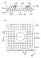
図12は、特許文献1に開示されている従来の樹脂封止型半導体装置に用いられるリードフレームの構造を示す図である。同図に示すように、この従来のリードフレームは、半導体チップを搭載するダイパッド1001と、その末端でフレーム枠1002と接続され、先端部でダイパッド1001の四隅を支持する吊りリード1003と、その先端部がダイパッド1001に対向し、末端部がフレーム枠1002に接続された直線状のランドリード1004及びリード1005とを有している。そして、ランドリード1004とリード1005との各底面部が外部端子(ランド部)を構成しており、リード1005はその底面に加えて外方の側面部でも外部端子として実装基板と接続できるように構成されている。また、ランドリード1004の先端部はリード1005の先端部を越えて、ダイパッド1001に近い部位まで延びている。
FIG. 12 is a diagram showing a structure of a lead frame used in a conventional resin-encapsulated semiconductor device disclosed in Patent Document 1. As shown in FIG. As shown in FIG. 1, this conventional lead frame includes a
ダイパッド1001には、その表面の略中央部分に上方に突出した円形の突出部1006が設けられ、突出部1006は、ダイパッド1001を構成している平板に対してプレス加工により半切断状態のプレスを施し、上方に突出させることにより形成されたものである。この突出部1006が実質的に半導体チップを支持する部分となり、半導体チップを搭載した際、ダイパッド1001の突出部1006を除く表面と半導体チップ裏面との間には間隙が形成される。ダイパッド1001の表面の突出部1006を包囲する領域には溝部1007が設けられ、半導体チップを搭載して樹脂封止した際に、封止樹脂がその溝部1007に入り込むように設けられている。
The
このような構成を有するリードフレームにより、半導体チップを搭載し、金属細線で半導体チップと各リードとを接続し、樹脂封止して樹脂封止型半導体装置を構成した際、樹脂封止型半導体装置の底面、すなわちパッケージ底面には、先端部が曲面となっているランド部1008の底面が配置され、そのランド部1008の外側にはリード1005の先端部が曲面となっている底面部分が配置されて千鳥状の2列配置の外部端子が構成されている。これにより、LGA(ランド・グリッド・アレイ)型パッケージを構成することができる。
しかしながら、従来のリードフレームによると、以下のような不具合があった。 However, the conventional lead frame has the following disadvantages.
従来のリードフレームにより、ランド部が複数列に配置されたLGAが得られるものの、ダイパッド1001を固定している吊りリード1003の存在する部位にはランド部を配置することができない。そのために、ランド部(端子電極)数を増やす場合の制約がある。
Although a conventional lead frame can provide an LGA in which lands are arranged in a plurality of rows, the lands cannot be arranged at a portion where the suspension leads 1003 fixing the
また、吊りリードが存在することから、このリードフレームを使用した半導体装置を作成するにあたって、樹脂封止の際にダイパッドと樹脂部との熱収縮率の差から、半導体装置に反りが発生していた。 Also, due to the presence of the suspension leads, when manufacturing a semiconductor device using this lead frame, the semiconductor device is warped due to the difference in the heat shrinkage between the die pad and the resin portion during resin sealing. Was.
さらにもう1つの問題として、シート貼り付け前の加工工程数が増加し、コストUPの要因となることが課題となっていた。 Still another problem is that the number of processing steps before sheet attachment is increased, which causes a cost increase.
本発明の目的は、半導体装置のさらなる多品種多端子化に対応し、生産性が高く安価で品質の良い樹脂封止型半導体装置の製造に適したリードフレーム、このようなリードフレームを用いた樹脂封止型半導体装置及びその製造方法を提供することにある。 An object of the present invention is to provide a lead frame suitable for the production of a resin-encapsulated semiconductor device with high productivity, inexpensiveness and high quality, which corresponds to a further increase in the number of types and terminals of the semiconductor device, and the use of such a lead frame. An object of the present invention is to provide a resin-encapsulated semiconductor device and a method for manufacturing the same.
本発明の第1のリードフレームは、上面がボンディングパッドとなり最下部が外部端子となる島部と、外枠−島部−島部−ダイパッド間を接続する連結部とを有するリードを設けると共に、樹脂封止時に吊りリードとして機能するリードをなくしたものである。 The first lead frame of the present invention is provided with a lead having an island portion having an upper surface serving as a bonding pad and a lowermost portion serving as an external terminal, and a connecting portion connecting an outer frame-island portion-island portion-die pad, The lead functioning as a suspension lead during resin sealing is eliminated.
これにより、通常はコーナー部に配置されていた吊りリードの代わりに外部端子を配置することができるので、外部端子を高密度に配置してなる樹脂封止型半導体装置が得られる。また、吊りリードが存在することによって生じやすいダイパッドの変形,移動などを抑制することができる。 As a result, the external terminals can be arranged instead of the suspension leads normally arranged at the corners, so that a resin-sealed semiconductor device in which the external terminals are arranged at a high density can be obtained. In addition, it is possible to suppress deformation, movement, and the like of the die pad, which are likely to be caused by the presence of the suspension leads.
各島部の最下部は、実質的に同一の平面形状を有していて、格子状に配置されていることにより、さらに高密度の実装が可能になる。 The lowermost portion of each island has substantially the same planar shape and is arranged in a grid, so that a higher density mounting is possible.
各島部の最下部は、上記外枠の各辺に沿って3列以上の複数列に配置されていることが好ましい。 It is preferable that the lowermost part of each island is arranged in a plurality of rows of three or more rows along each side of the outer frame.
本発明の第2のリードフレームは、ダイパッドの外周部に下部が欠如した薄膜部と薄膜部の下面から下方に突出する放熱端子とを設けるとともに、上面がボンディングパッドとなり最下部が外部端子となる島部と、外枠−島部−島部−放熱端子間を接続する連結部とを有するリードを設けたものである。 In the second lead frame of the present invention, a thin-film portion having a lower portion and a heat-radiating terminal projecting downward from the lower surface of the thin-film portion are provided on the outer peripheral portion of the die pad, and the upper surface becomes a bonding pad and the lowermost portion becomes an external terminal. A lead having an island portion and a connecting portion for connecting the outer frame, the island portion, the island portion, and the heat radiation terminal is provided.
これにより、このリードフレームを用いた樹脂封止型半導体装置を形成した後、樹脂封止型半導体装置をマザーボードに搭載する際には、外部端子と放熱端子とを半田の一括リフローによってマザーボードの電極などと接続できるので、実装の安定化,容易化を図ることができる。 Thus, after the resin-encapsulated semiconductor device using the lead frame is formed, when mounting the resin-encapsulated semiconductor device on the motherboard, the external terminals and the heat dissipation terminals are connected to the electrodes of the motherboard by the batch reflow of solder. And so on, so that mounting can be stabilized and facilitated.
各島部及び各放熱端子は、実質的に同一の平面形状を有していて、格子状に配置されていることにより、さらに高密度の実装が可能になる。 Each of the island portions and each of the heat radiation terminals have substantially the same planar shape, and are arranged in a lattice, so that a higher density mounting is possible.
各島部及び各放熱端子は、少なくとも1つの方向において実質的に一定のピッチで配置されていることが好ましく、各島部は、上記外枠の各辺に沿って3列以上の複数列に配置されていることが好ましい。 It is preferable that each island portion and each heat radiation terminal are arranged at a substantially constant pitch in at least one direction, and each island portion is arranged in a plurality of rows of three or more rows along each side of the outer frame. Preferably, they are arranged.
本発明の第1の樹脂封止型半導体装置は、第1のリードフレームを用いて形成されたものであって、上面が金属細線を接続するためのボンディングパッドであり最下部が外部端子である島部と、島部の最下部とダイパッドの底面の少なくとも一部とを露出させた状態で、半導体チップ,島部,ダイパッド等を封止する封止樹脂とを備え、ダイパッドから延びて、先端部が封止樹脂の表面に露出する部材は設けられていない。 The first resin-encapsulated semiconductor device of the present invention is formed using a first lead frame. The upper surface is a bonding pad for connecting a thin metal wire, and the lowermost portion is an external terminal. An island portion, and a sealing resin for sealing the semiconductor chip, the island portion, the die pad, and the like in a state where the lowermost portion of the island portion and at least a part of the bottom surface of the die pad are exposed; No member whose part is exposed on the surface of the sealing resin is provided.
これにより、通常はコーナー部に配置されていた吊りリードの代わりに外部端子を配置することができるので、外部端子を高密度に配置してなる樹脂封止型半導体装置が得られる。 As a result, the external terminals can be arranged instead of the suspension leads normally arranged at the corners, so that a resin-sealed semiconductor device in which the external terminals are arranged at a high density can be obtained.
各外部端子は、実質的に同一の平面形状を有していて、封止樹脂の裏面に格子状に配置されていることにより、さらに高密度の実装が可能になる。 The external terminals have substantially the same planar shape, and are arranged in a lattice on the back surface of the sealing resin, so that higher-density mounting is possible.
各外部端子は、外周に沿って封止樹脂の裏面に3列以上の複数列に配置されていることが好ましい。 It is preferable that the external terminals are arranged in three or more rows on the back surface of the sealing resin along the outer periphery.
本発明の第2の樹脂封止型半導体装置は、第2のリードフレームを用いて形成されたものであって、本体部の外周部に沿って設けられ下部が欠如した薄膜部と、薄膜部の下面から下方に突出するように設けられた複数の放熱端子とを有するダイパッドと、上面が金属細線を接続するためのボンディングパッドであり最下部が外部端子である島部と、島部の最下部と及び放熱端子の最下部とを露出させた状態で、半導体チップ,島部,リード,ダイパッド等を封止する封止樹脂とを備えている。 A second resin-encapsulated semiconductor device according to the present invention is formed using a second lead frame, and includes a thin film portion provided along an outer peripheral portion of a main body portion and lacking a lower portion; A die pad having a plurality of heat dissipating terminals provided so as to protrude downward from the lower surface of the die, an island portion having an upper surface serving as a bonding pad for connecting a thin metal wire, and a lowermost portion serving as an external terminal; A sealing resin that seals the semiconductor chip, the island, the leads, the die pad, and the like with the lower portion and the lowermost portion of the heat radiation terminal exposed.
これにより、樹脂封止型半導体装置をマザーボードに搭載する際には、外部端子と放熱端子とを半田の一括リフローによってマザーボードの電極などと接続できるので、実装の安定化,容易化を図ることができる。 As a result, when the resin-encapsulated semiconductor device is mounted on the motherboard, the external terminals and the heat dissipation terminals can be connected to the electrodes of the motherboard by batch reflow of the solder, thereby stabilizing and facilitating the mounting. it can.
各外部端子及び各放熱端子は、実質的に同一の平面形状を有していて、封止樹脂の裏面に格子状に配置されていることにより、実装の容易化と高密度実装とを実現することができる。 Each external terminal and each heat radiation terminal have substantially the same planar shape and are arranged in a lattice on the back surface of the sealing resin, thereby facilitating mounting and achieving high-density mounting. be able to.
各外部端子及び各放熱端子は、少なくとも1つの方向において実質的に一定のピッチで配置されていることが好ましく、各外部端子は、外周に沿って封止樹脂の裏面に3列以上の複数列に配置されていることが好ましい。 Each external terminal and each heat radiation terminal are preferably arranged at a substantially constant pitch in at least one direction, and each external terminal is provided in three or more rows on the back surface of the sealing resin along the outer periphery. Are preferably arranged.
本発明の第1の樹脂封止型半導体装置の製造方法は、上記第1のリードフレームを準備した後、ダイボンド工程と、封止シート上でのリードフレームの連結部の分断工程とを行なってから、電気的接続と、封止シートをリードフレームにつけたままでの樹脂封止を行なう方法である。 According to the first method of manufacturing a resin-encapsulated semiconductor device of the present invention, after preparing the first lead frame, a die bonding step and a step of cutting a connecting portion of the lead frame on the sealing sheet are performed. Therefore, it is a method of performing electrical connection and resin sealing with the sealing sheet attached to the lead frame.
この方法により、吊りリードがなくても、ダイパッドや島部の位置を安定化させて、電気的接続,樹脂封止を行なうことができ、外部端子を高密度に配置した樹脂封止型半導体装置が得られる。 According to this method, the position of the die pad and the island portion can be stabilized, the electrical connection and the resin sealing can be performed without the suspension leads, and the resin-encapsulated semiconductor device in which external terminals are arranged at a high density. Is obtained.
本発明の第2の樹脂封止型半導体装置の製造方法は、上記第2のリードフレームを準備した後、ダイボンド工程と、封止シート上でのリードフレームの連結部の分断工程とを行なってから、電気的接続と、封止シートをリードフレームにつけたままでの樹脂封止を行なう方法である。 According to the second method of manufacturing a resin-encapsulated semiconductor device of the present invention, after preparing the second lead frame, a die bonding step and a step of cutting a connecting portion of the lead frame on the sealing sheet are performed. Therefore, it is a method of performing electrical connection and resin sealing with the sealing sheet attached to the lead frame.
この方法により、ダイパッドや島部の位置を安定化させて、電気的接続,樹脂封止を行なうことができ、放熱端子を外部端子と共に並べて封止樹脂の裏面に突出させることができ、マザーボードへの実装が容易な樹脂封止型半導体装置が得られる。 By this method, the position of the die pad and the island portion can be stabilized, electrical connection and resin sealing can be performed, and the heat radiation terminals can be arranged along with the external terminals and projected on the back surface of the sealing resin, so that the motherboard can be mounted. A resin-encapsulated semiconductor device that is easy to mount is obtained.
本発明の第1のリードフレーム,これを用いた樹脂封止型半導体装置及びその製造方法によると、吊りリードがない分だけ、外部端子を高密度に設けた樹脂封止型半導体装置を得ることが可能になる。 According to the first lead frame of the present invention, the resin-encapsulated semiconductor device using the same, and the method of manufacturing the same, it is possible to obtain a resin-encapsulated semiconductor device in which external terminals are provided at a high density because of no suspension leads. Becomes possible.
本発明の第2のリードフレーム,これを用いた樹脂封止型半導体装置及びその製造方法によると、ダイパッドに外部端子と共に並ぶ放熱端子を設けたので、実装の容易化を図ることが可能になる。 According to the second lead frame of the present invention, the resin-encapsulated semiconductor device using the same, and the method of manufacturing the same, the heat dissipation terminals are provided on the die pad along with the external terminals, so that the mounting can be facilitated. .
(第1の実施形態)
−リードフレームの構造−
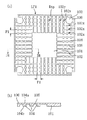
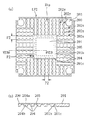
図1(a),(b)は、それぞれ順に、本発明の第1の実施形態に係るリードフレームの平面図、及び図1(a)のIB−IB線における断面図である。図1(a)は、多数の半導体チップを搭載する領域が碁盤目状に連続して設けられているリードフレームLF1の一部、つまり、1つの半導体チップを搭載する領域だけを抜き出して示している。リードフレームLF1は、銅合金板をエッチング,打ち抜きプレス等によって加工して得られるものである。
(1st Embodiment)
-Lead frame structure-
FIGS. 1A and 1B are a plan view of a lead frame according to the first embodiment of the present invention and a cross-sectional view taken along line IB-IB of FIG. 1A, respectively. FIG. 1A shows only a part of a lead frame LF1 in which regions for mounting a large number of semiconductor chips are continuously provided in a grid pattern, that is, only a region for mounting one semiconductor chip. I have. The lead frame LF1 is obtained by processing a copper alloy plate by etching, punching press, or the like.
図1(a),(b)に示すように、本実施形態のリードフレームLF1は、チップ搭載領域Rtpを囲む,4つの辺からなる矩形状の外枠100と、チップ搭載領域Rtpの中央部に設けられた半導体チップ搭載用のダイパッド101と、外枠100から延びてダイパッド101につながるリード102と、補強用ランド103とを備えている。
As shown in FIGS. 1A and 1B, the lead frame LF1 of the present embodiment has a rectangular
本実施形態のリード102は、広幅(例えば20μm〜120μm)かつ厚肉(例えば20μm〜120μm)の島部104と、細幅(例えば15μm〜100μm)かつ薄肉(例えば15μm〜100μm)の連結部105とを交互に配置して構成されている。島部104の上面は金属細線が接続されるボンディングパッド104aとして機能する。また、半導体チップをリードフレームLF1上に実装する工程において、島部104の下面が接着層を有する封止シートに固定された状態で樹脂封止され、島部104の最下部が樹脂封止後に封止樹脂の裏面から下方に突出したランド電極104b(外部端子)として機能する。連結部105は、外枠100と島部104との間,島部104同士の間,及び島部104とダイパッド101との間をそれぞれ接続している。連結部105は、金型によるプレス加工またはエッチング加工によりその下部が欠如しており、半導体チップをリードフレームLF1上に実装する工程において封止樹脂内に埋め込まれる部分である。連結部105は、島部104の上部と連続していて、連結部105の上面は島部104の上面と共通の平面を構成している。
The
ここで、本実施形態のリードフレームLF1の特徴について説明する。本実施形態のリードフレームLF1には、通常のリードフレームには存在している,吊りリードとしての機能しかない部材が存在していない。つまり、島部104が設けられていないリードは存在しない。したがって、本実施形態のリードフレームLF1のダイパッドは、樹脂封止工程の際には、外枠に接続されておらず、樹脂封止工程時における吊りリードとして機能するリードは設けられていない。つまり、樹脂封止型半導体装置内には、ダイパッド101から延びて、封止樹脂の表面に露出するリードは存在しない。
Here, features of the lead frame LF1 of the present embodiment will be described. In the lead frame LF1 of the present embodiment, there is no member existing only in a normal lead frame and having only a function as a suspension lead. That is, there is no lead in which the
そして、本実施形態のリードフレームLF1においては、ダイパッド101のコーナー部と外枠100のコーナー部とを結ぶ線上にも、島部104(つまり,ボンディングパッド104a及びランド電極104b)が配置されている。また、本実施形態のリードフレームLF1には、コーナー部付近において、当該リードが接続される外枠100の一辺に隣接する他の辺から延びるリード102y(又は102x)に連結されているリード102x(又は102y)が存在する。つまり、他のリード102y(又は102x)を介してダイパッド101に接続されるリード102x(又は102y)が存在している。さらに、本実施形態のリードフレームLF1においては、コーナー部において外枠100に直接接続される、島部104よりも遙かに大面積(例えば、径300μmから1500μm)の補強用ランド103が設けられている。
In the lead frame LF1 of the present embodiment, the islands 104 (that is, the
そして、各島部104の最下部である各ランド電極(外部端子)104bは、実質的に同じ平面形状を有しており、格子状に配列されている。ここで、「実質的に同じ」とは、製造時のばらつきを考慮しない場合に同じであるという意味である。
Each land electrode (external terminal) 104b at the lowermost part of each
本実施形態のリードフレームLF1によると、コーナー部において、吊りリードを設けずに、外枠100の相隣接する2つの辺から延びるリード同士を連結させることにより、コーナー部も含めてランド電極104b(外部端子)を外枠100の各辺に沿って複数列に配置した樹脂封止型半導体装置を形成することが可能になる。すなわち、従来のリードフレームのようにコーナー部に吊りリードが存在する場合には、吊りリードの途中にランド電極を設けることはできるものの、吊りリードがダイパッドに接続されているので、吊りリードの途中のランド電極は、単なる補強用か、ダイパッドと同電位になる端子用に限られる(例えば、接地端子など)。それに対し、本実施形態のリードフレームLF1においては、信号端子として機能するランド電極をコーナー部にまで配置することができ、ランド電極を高密度に配置することが可能になる。言い換えると、ランド電極の配置場所や数に関する制約を緩和することができる。
According to the lead frame LF1 of the present embodiment, the leads extending from two adjacent sides of the
また、後に説明するように、本実施形態のリードフレームLF1を用いて樹脂封止を行なう工程において、各ランド電極104(島部102)とダイパッド101とは互いに接続されることなく離間した状態で封止シートによってそれぞれ支持されているので、リードフレーム本体と封止樹脂との熱収縮率の差によって発生する反りが個々に分断され、半導体装置全体としての反り量を低減することができる。
As described later, in the step of performing resin sealing using the lead frame LF1 of the present embodiment, each land electrode 104 (island 102) and the
また、本実施形態のリードフレームLF1は、コーナー部に大型の円形パターンである補強用ランド103が設けられているので、樹脂封止型半導体装置をマザーボード上に実装(2次実装)する際に、樹脂封止型半導体装置と、マザーボードとの間のはんだ等による接合強度の向上を図ることができる。
Further, the lead frame LF1 of the present embodiment is provided with the reinforcing
ただし、本実施形態のリードフレームLF1における補強用ランド103は、必ずしも設ける必要がない。補強用ランド103が存在しない場合には、そのスペースにランド電極(島部)を配置することができるので、ランド電極をさらに高密度に配置することが可能になる。
However, the reinforcing
−樹脂封止型半導体装置の製造工程−
次に、本実施形態のリードフレームLF1を用いた樹脂封止型半導体装置の製造工程の一例について説明する。図2(a),(b)は、第1の実施形態の樹脂封止型半導体装置の製造工程のうちダイパッドの中央部をアップセットする工程を示す平面図及びIIB−IIB線における断面図である。図3(a),(b)は、第1の実施形態の樹脂封止型半導体装置の製造工程のうちのリードフレームを封止シート上に載置する工程を示す平面図及びIIIB−IIIB線における断面図である。図4(a),(b)は、第1の実施形態の樹脂封止型半導体装置の製造工程のうちリードを分断する工程を示す平面図及びIVB−IVB線における断面図である。図5は、第1の実施形態の樹脂封止型半導体装置の製造工程のうち樹脂封止工程を示す部分断面図である。図6(a),(b)は、第1の実施形態の樹脂封止型半導体装置の樹脂封止工程終了後における構造を示すVIA−VIA線における断面図及び裏面図である。
-Manufacturing process of resin-encapsulated semiconductor device-
Next, an example of a manufacturing process of the resin-encapsulated semiconductor device using the lead frame LF1 of the present embodiment will be described. FIGS. 2A and 2B are a plan view and a cross-sectional view taken along line IIB-IIB, respectively, showing a step of upsetting a central portion of a die pad in a manufacturing process of the resin-sealed semiconductor device according to the first embodiment. is there. FIGS. 3A and 3B are a plan view and a IIIB-IIIB line showing a step of mounting a lead frame on a sealing sheet in the manufacturing steps of the resin-encapsulated semiconductor device of the first embodiment. FIG. FIGS. 4A and 4B are a plan view and a cross-sectional view taken along the line IVB-IVB, respectively, showing a step of dividing the leads in the manufacturing steps of the resin-sealed semiconductor device of the first embodiment. FIG. 5 is a partial cross-sectional view showing a resin sealing step in the manufacturing steps of the resin-sealed semiconductor device of the first embodiment. FIGS. 6A and 6B are a cross-sectional view and a rear view taken along the line VIA-VIA showing the structure of the resin-sealed semiconductor device of the first embodiment after the resin sealing step.
まず、図2(a),(b)に示す工程で、銅(Cu)を主成分とする合金または鉄(Fe)およびニッケル(Ni)の合金からなる金属板をスタンピングまたはエッチングにより一体成形して、図1(a),(b)に示す構造を有するリードフレームLF1を用意する。次に、上部半切断金型と下部プレス金型と(いずれも図示せず)を用いて、リードフレームLF1をプレス加工することにより、ダイパッド101に円形の突出部101aを形成する。この工程は、半導体チップをアップセットしてダイパッド101上に支持することを目的としているが、必ずしも突出部101aを設ける必要はない。また、リードフレームLF1には、半導体チップとの接合や実装に必要なめっきが部分的または全面に施される。めっきの種類としては、Agめっき,Auめっき,Ni−Pd−Auめっきなどを用いることができる。
First, in a process shown in FIGS. 2A and 2B, a metal plate made of an alloy mainly containing copper (Cu) or an alloy of iron (Fe) and nickel (Ni) is integrally formed by stamping or etching. Then, a lead frame LF1 having the structure shown in FIGS. 1A and 1B is prepared. Next, a
次に、図3(a),(b)に示す工程で、リードフレームLF1の裏面、つまり、ダイパッド101の本体部,補強用ランド103,島部104の各下面に密着するように封止シート150を貼り付ける。封止シート150の上面には接着層が設けられており、この接着層により、ダイパッド101,補強用ランド103及びリード102の島部104が、孤立した状態で封止シート150上に固定されている。
Next, in the steps shown in FIGS. 3A and 3B, the sealing sheet is adhered to the back surface of the lead frame LF1, that is, the lower surface of the main body of the
次に、図4(a),(b)に示す工程で、封止シート150上にリードフレームLF1を固定した状態で、金型を用いたプレス加工により、リード102を切断部Ct1,Ct2,Ct3で分断する。すなわち、リード102の島部104とダイパッド101との間の連結部105,島部104同士の間の連結部105,及び島部104と外枠100との間の連結部105をそれぞれ切断して、ダイパッド101及び各島部104を孤立させる。
Next, in the steps shown in FIGS. 4A and 4B, in a state where the lead frame LF1 is fixed on the
次に、工程の図示は省略するが、リードフレームLF1を封止シート150に載置した状態で、リードフレームLF1の各チップ搭載領域Rtpのダイパッド101上に半導体チップ160をそれぞれ搭載し(ダイボンド工程)、半導体チップ160のパッド電極と島部104のボンディングパッド104aとを接続部材である金属細線170によって接続する(ワイヤボンディング工程)。
Next, although illustration of the process is omitted, the
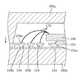
そして、図5に示すように、ダイキャビティを有する上型180aと下型180bとからなる封止金型にリードフレームLF1をセットする。すなわち、ダイキャビティに半導体チップ150,金属細線170等が入り込むように、リードフレームLF1を封止金型にセットし、上型180aと下型180bとの間を押圧した状態で、ダイキャビティ内に封止樹脂を充填する。
Then, as shown in FIG. 5, the lead frame LF1 is set in a sealing die including an
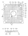
そして、樹脂封止工程の終了後に、封止シート150をリードフレームLF1や封止樹脂から引き剥がしてから、リードフレームLF1上に形成されている多数の樹脂封止型半導体装置を、個々に切り出すことにより、図6(a),(b)に示す構造を有する樹脂封止型半導体装置が得られる。ただし、図6(a)に示す断面図においては、右半分の横方向寸法は左半分の横方向寸法と同じ寸法に縮小されている。
After the resin sealing step is completed, the sealing
図6(a),(b)に示すように、リードフレームLF1の島部104の最下部であるランド電極104b,ダイパッド101の最下部,及び補強用ランド103の最下部が封止樹脂190から下方に突出している。特に、ランド電極104bは、図6(b)における縦方向及び横方向に一定のピッチ(間隔)P1で複数列に配置されており、コーナー部にも配置されていることがわかる。そして、樹脂封止型半導体装置内には、ダイパッド101から延びて、封止樹脂の表面に露出するリードは存在しない。
As shown in FIGS. 6A and 6B, the
ランド電極104b同士の間隔は必ずしも一定である必要はなく、かつ、一定のピッチで配置されている場合でも、図6(b)における縦方向と横方向とでピッチが異なっていてもよいが、このように一定のピッチでランド電極104bが配置されていることにより、現実の半導体装置の規格に適合した樹脂封止型半導体装置が得られる。
The interval between the
本実施形態の樹脂封止型半導体装置によると、従来存在していた吊りリードをなくすとともに、ダイパッド101とリード102の島部104との間、リード102中の各島部104同士の間,島部104と外枠100との間に、島部104よりも狭幅,薄肉の連結部105を介在させているので、図4(a),(b)に示す工程において、リードフレームLF1に半導体チップ160を搭載した状態で、リード102中の各島部104同士の間,島部104と外枠100との間を容易に切断して、ダイパッド101と外枠100との間を接続する部材が存在しない状態で、ワイヤボンディング工程を行ったり、樹脂封止工程を行なうことができる。
According to the resin-encapsulated semiconductor device of the present embodiment, the suspending lead which has conventionally existed is eliminated, and between the
したがって、吊りリードを形成するためのエッチング、型抜き等の手間が省けるとともに、図6(a),(b)に示すように、ランド電極104bが高密度に配置された樹脂封止型半導体装置が得られることになる。
Therefore, it is possible to save the time and labor of etching and die cutting for forming the suspension leads, and as shown in FIGS. 6A and 6B, the resin-encapsulated semiconductor device in which the
(第2の実施形態)
図7(a),(b)は、それぞれ順に、本発明の第2の実施形態に係るリードフレームの平面図、及びVIIB−VIIB線における断面図である。図7(a)は、多数の半導体チップを搭載する領域が碁盤目状に連続して設けられているリードフレームLF2の一部、つまり、1つの半導体チップを搭載する領域だけを抜き出して示している。リードフレームLF2は、銅合金板をエッチング,打ち抜きプレス等によって加工して得られるものである。
(Second embodiment)
FIGS. 7A and 7B are a plan view of a lead frame according to a second embodiment of the present invention and a cross-sectional view taken along the line VIIB-VIIB, respectively. FIG. 7A shows a part of a lead frame LF2 in which regions for mounting a large number of semiconductor chips are continuously provided in a grid pattern, that is, only a region for mounting one semiconductor chip. I have. The lead frame LF2 is obtained by processing a copper alloy plate by etching, punching press, or the like.
図7(a),(b)に示すように、本実施形態のリードフレームLF2は、チップ搭載領域Rtpを囲む,4つの辺からなる矩形状の外枠200と、チップ搭載領域Rtpの中央部に設けられた半導体チップ搭載用のダイパッド201と、外枠200から延びてダイパッド201につながるリード202と、補強用ランド203と、ダイパッド201の外周部に設けられリード202につながる放熱端子201bとを備えている。
As shown in FIGS. 7A and 7B, the lead frame LF2 of the present embodiment includes a rectangular
本実施形態のリード202は、広幅(例えば20μm〜120μm)かつ厚肉(例えば20μm〜120μm)の島部204と、細幅(例えば15μm〜100μm)かつ薄肉(例えば15μm〜100μm)の連結部205とを交互に配置して構成されている。島部204の上面は、金属細線が接続されるボンディングパッド204aとして機能する。また、半導体チップをリードフレームLF2上に実装する工程において、島部204の下面が接着層を有する封止シートに固定された状態で樹脂封止され、島部204の最下部が樹脂封止後に封止樹脂の裏面から下方に突出したランド電極204bとして機能する。連結部205は、外枠200と島部204との間,島部204同士の間,及び島部204とダイパッド201の放熱端子201bとの間をそれぞれ接続している。連結部205は、金型によるプレス加工またはエッチング加工によりその下部が欠如しており、半導体チップをリードフレームLF2上に実装する工程において封止樹脂内に埋め込まれる。連結部205は、島部204の上部と連続していて、連結部205の上面は島部204の上面と共通の平面を構成している。
The lead 202 of the present embodiment includes a wide (eg, 20 μm to 120 μm) and thick (eg, 20 μm to 120 μm)
ここで、本実施形態のリードフレームLF2の特徴について説明する。本実施形態のリードフレームLF2には、通常のリードフレームには存在している,ダイパッドを支える機能だけを有する吊りリードが存在していない。また、本実施形態のリードフレームLF2のダイパッドは、樹脂封止工程の際には、分断されているリード202のみによって外枠に接続されているので、樹脂封止工程の際に吊りリードとして機能するリードは設けられていない。そして、本実施形態のリードフレームLF2においては、ダイパッド201のコーナー部と外枠200のコーナー部とを結ぶ線上にも、島部204(つまり,ボンディングパッド204a及びランド電極204b)が配置されている。また、本実施形態のリードフレームLF2には、コーナー部付近において、ダイパッド201に直接接続されずに、当該リード202x(又は202y)が接続される外枠200の一辺に隣接する他の辺から延びるリード202y(又は202x)に連結されているリード202x(又は202y)が存在する。つまり、当該リード202x(又は202y)が接続される外枠200の一辺に隣接する他の辺から延びるリード202y(又は202x)を介してダイパッド201に接続されるリード202x(又は202y)が存在している。さらに、本実施形態のリードフレームLF2においては、外枠200に近いコーナー部において、島部204よりも遙かに大面積(例えば、径300μmから1500μm)の補強用ランド203が設けられている。
Here, features of the lead frame LF2 of the present embodiment will be described. In the lead frame LF2 of the present embodiment, there is no suspension lead having only a function of supporting the die pad, which is present in a normal lead frame. Further, the die pad of the lead frame LF2 of the present embodiment is connected to the outer frame only by the separated leads 202 in the resin sealing step, and thus functions as a suspension lead in the resin sealing step. No lead is provided. In the lead frame LF2 of the present embodiment, the islands 204 (that is, the
本実施形態のリードフレームLF2は、第1の実施形態のリードフレームLF1と同じ特徴に加えて、以下のような特徴を有している。すなわち、ダイパッド201の外周部は、下部が欠如した薄膜部201cとなっており、薄膜部201cの下面から下方に突出した放熱端子201bが設けられている。このような形状は、ハーフエッチング又はプレス加工によって、ダイパッド201の外周部を放熱端子201bとなる部分を残して下部を欠如させることにより、形成される。
The lead frame LF2 of the present embodiment has the following features in addition to the same features as the lead frame LF1 of the first embodiment. In other words, the outer peripheral portion of the
本実施形態においては、各島部204の最下部である各ランド電極(外部端子)204bと、放熱端子201bの最下部とは、実質的に同じ平面形状を有しており、格子状に配列されている。ここで、「実質的に同じ」とは、製造時のばらつきを考慮しない場合に同じであるという意味である。ただし、必ずしも各島部204の最下部である各ランド電極(外部端子)204bと、放熱端子201bの最下部とが、実質的に同じ平面形状を有していなくても、後述する基本的な効果を発揮することは可能である。
In the present embodiment, each land electrode (external terminal) 204b, which is the lowermost part of each
この放熱端子201bが設けられていることにより、本実施形態のリードフレームにより、第1の実施形態と同じ効果に加えて、以下のような格別の効果を発揮することができる。 By providing the heat radiating terminal 201b, the lead frame of the present embodiment can exhibit the following special effects in addition to the same effects as the first embodiment.
第1の実施形態のリードフレームLF1を用いてLGA(ランドグリッドアレイ)構造を持つ樹脂封止型半導体装置の製造工程において、リード102の島部104とダイパッド101との間を打ち抜き加工により切断すると、切断の後にリードの変形という不具合が発生するおそれがあった。そこで、これを回避するために、図1(a),(b)に示すように、島部104とダイパッド101との間の連結部105を、島部104同士の間の連結部105よりも長くする必要があった。しかし、今後、ランド電極数が増えるに従って、抜き形状の複雑化によってさらに変形しやすく、生産性を悪化させるおそれがある。
In the manufacturing process of the resin-encapsulated semiconductor device having the LGA (land grid array) structure using the lead frame LF1 of the first embodiment, the space between the
ところが、本実施形態のように、ダイパッド201に放熱端子201bを設けることにより、後述するリード202の切断工程において、リード202の変形を抑制しつつ,円滑に島部204及びダイパッド201を外枠200から切り離すことが可能になる。その結果、リード202の最先端の島部204と放熱端子201bとを接続する連結部205を短くできるので、島部204(ランド電極204b)をより高密度に配置することができる。
However, as in the present embodiment, by providing the
また、放熱端子201bの存在により、後述する樹脂封止型半導体装置をマザーボード上に実装する際に、接合不良が生じやすいダイパッド201の本体部をマザーボードに接合せずに、半田の一括リフローにより、放熱端子201bのみをランド電極204bと共にマザーボードの電極などに接合させることができる。そして、ダイパッド201の本体部とマザーボードとの接合を行なわなくても、放熱端子201bにより、半導体チップの発熱をマザーボードに速やかに逃すことができる。本実施形態では、放熱機能が放熱面積がある面積以上になると飽和することを考慮して、複数の放熱端子201bの下面の合計面積は、半導体チップの発熱を速やかにマザーボード側に逃して半導体チップ内の半導体素子の機能が損なわれないように設定されている。よって、本実施形態のリードフレームを用いた樹脂封止型半導体装置の放熱機能は、第1の実施形態と同等に維持することができる。
Also, due to the presence of the
−樹脂封止型半導体装置の製造工程−
次に、本実施形態のリードフレームLF2を用いた樹脂封止型半導体装置の製造工程の一例について説明する。図8(a),(b)は、第2の実施形態の樹脂封止型半導体装置の製造工程のうちダイパッドの中央部をアップセットしてリードフレームを封止シート上に載置する工程を示す平面図及びVIIIB−VIIIB線における断面図である。図9(a),(b)は、第2の実施形態の樹脂封止型半導体装置の製造工程のうちリードを分断する工程を示す平面図及びIXB-IXB線における断面図である。図10(a),(b)は、第2の実施形態の樹脂封止型半導体装置の樹脂封止工程終了後における構造を示すXA−XA線における断面図及び裏面図である。
-Manufacturing process of resin-encapsulated semiconductor device-
Next, an example of a manufacturing process of a resin-sealed semiconductor device using the lead frame LF2 of the present embodiment will be described. FIGS. 8A and 8B show a process of upsetting a central portion of a die pad and mounting a lead frame on a sealing sheet in the manufacturing process of the resin-encapsulated semiconductor device of the second embodiment. It is the top view shown and sectional drawing in the VIIIB-VIIIB line. FIGS. 9A and 9B are a plan view and a cross-sectional view taken along line IXB-IXB, respectively, showing a step of dividing the leads in the manufacturing steps of the resin-sealed semiconductor device according to the second embodiment. FIGS. 10A and 10B are a cross-sectional view and a rear view taken along the line XA-XA showing the structure of the resin-sealed semiconductor device of the second embodiment after the resin sealing step is completed.
まず、図8(a),(b)に示す工程で、銅(Cu)を主成分とする合金または鉄(Fe)およびニッケル(Ni)の合金からなる金属板をスタンピングまたはエッチングにより一体成形して、図7(a),(b)に示す構造を有するリードフレームLF2を用意する。次に、上部半切断金型と下部プレス金型と(いずれも図示せず)を用いて、リードフレームLF2をプレス加工することにより、ダイパッド201に円形の突出部201aを形成する。この工程は、半導体チップをアップセットしてダイパッド201上に支持することを目的としているが、必ずしも突出部201aを設ける必要はない。。また、リードフレームLF2には、半導体チップとの接合や実装に必要なめっきが部分的または全面に施される。めっきの種類としては、Agめっき,Auめっき,Ni−Pd−Auめっきなどを用いることができる。
First, in steps shown in FIGS. 8A and 8B, a metal plate made of an alloy mainly containing copper (Cu) or an alloy of iron (Fe) and nickel (Ni) is integrally formed by stamping or etching. Then, a lead frame LF2 having the structure shown in FIGS. 7A and 7B is prepared. Next, a
次に、リードフレームLF2の裏面、つまり、ダイパッド201,補強用ランド203,島部204の各下面に密着するように封止シート250を貼り付ける。封止シート250の上面には接着層が設けられており、この接着層により、ダイパッド201の本体部,ダイパッド201の放熱端子201b,補強用ランド203及びリード202の島部204が、孤立した状態で封止シート250上に固定されている。
Next, a sealing
次に、図9(a),(b)に示す工程で、封止シート250上にリードフレームLF2を固定した状態で、金型を用いたプレス加工により、リード202の島部204とダイパッド201の放熱端子201bとの間の連結部205,島部204同士の間の連結部205,及び島部204と外枠200との間の連結部205をそれぞれ切断して、ダイパッド201及び各島部204を孤立させる。このとき、ダイパッド201と外枠200とを接続する部材は存在していない。
Next, in the steps shown in FIGS. 9A and 9B, the
次に、工程の図示は省略するが、リードフレームLF2を封止シート250に載置した状態で、リードフレームLF2の各チップ搭載領域Rtpのダイパッド201上に半導体チップ260をそれぞれ搭載し(ダイボンド工程)、半導体チップ260のパッド電極と島部204のボンディングパッド204aとを接続部材である金属細線270によって接続する(ワイヤボンディング工程)。
Next, although illustration of the process is omitted, the
そして、第1の実施形態における図5に示す工程と同様に、ダイキャビティを有する上型180aと下型180bとからなる封止金型にリードフレームLF2をセットする。すなわち、ダイキャビティに半導体チップ260,金属細線270等が入り込むように、リードフレームLF2を封止金型にセットし、上型180aと下型180bとの間を押圧した状態で、ダイキャビティ内に封止樹脂を充填する。
Then, similarly to the process shown in FIG. 5 in the first embodiment, the lead frame LF2 is set in a sealing mold including an
そして、樹脂封止工程の終了後に、封止シート250をリードフレームLF2や封止樹脂から引き剥がしてから、リードフレームLF2上に形成されている多数の樹脂封止型半導体装置を、個々に切り出すことにより、図10(a),(b)に示す構造を有する樹脂封止型半導体装置が得られる。ただし、図10(a)に示す断面図においては、右半分の横方向寸法は左半分の横方向寸法と同じ寸法に縮小されている。
After the resin sealing step is completed, the sealing
図10(a),(b)に示すように、リードフレームLF2の島部204の最下部であるランド電極204b,ダイパッド201の本体部の最下部,ダイパッド201の放熱端子201bの最下部,及び補強用ランド203の最下部が封止樹脂290から下方に突出している。特に、放熱端子201b及びランド電極204bは、図10(b)における縦方向及び横方向に一定のピッチ(間隔)P2で3列以上の複数列に配置されており、コーナー部にも配置されていることがわかる。
As shown in FIGS. 10A and 10B, a
その後、樹脂封止型半導体装置をマザーボード上に実装する際には、ランド電極204b及び放熱端子201bを半田リフローによってマザーボードの各電極に接続すればよく、ダイパッド201の本体部をマザーボードに接続する必要はない。
Thereafter, when mounting the resin-encapsulated semiconductor device on the motherboard, the
本実施形態の樹脂封止型半導体装置によると、従来存在していた吊りリードをなくすとともに、ダイパッド201とリード202の島部204との間、リード202中の各島部204同士の間,島部204と外枠200との間に、島部204よりも狭幅,薄肉の連結部205を介在させているので、図9(a),(b)に示す工程において、リードフレームLF2に半導体チップ260を搭載した状態で、リード202中の各島部204同士の間,島部204と外枠200との間を容易に切断して、ダイパッド201と外枠200との間を接続する部材が存在しない状態で、ワイヤボンディング工程を行ったり、樹脂封止工程を行なうことができる。
According to the resin-encapsulated semiconductor device of the present embodiment, the suspending lead which has conventionally existed is eliminated, and the space between the
したがって、吊りリードを形成するためのエッチング、型抜き等の手間が省けるとともに、すでに説明したように、放熱端子201bを設けたことによって、ランド電極204bを第1の実施形態よりもさらに高密度に配置することができる。
Therefore, it is possible to save the work of etching, die-cutting and the like for forming the suspension lead, and as described above, the provision of the
また、ダイパッド201に放熱端子201bが設けられていることことにより、樹脂封止型はその実装工程において、半田の一括リフローにより、放熱端子201bをランド電極204bと共にマザーボードの電極などに接合させることが可能になった。すなわち、樹脂封止型半導体装置の実装の際に、放熱のためにダイパッド201の本体部をマザーボードに接続する必要がなくなったので、接続不良の低減を図ることができ、放熱性を高く維持しつつ,実装の容易化を図ることができる。
Further, since the
放熱端子201bとランド電極204bとの間隔,及びランド電極204b同士の間隔は必ずしも一定である必要はなく、かつ、一定のピッチで配置されている場合でも、図10(b)における縦方向と横方向とでピッチが異なっていてもよい。しかし、特に、放熱端子201bと島部204とが実質的に同じ平面形状を有し、放熱端子201bと島部204との間の連結部205が、島部204同士の間の連結部205と実質的に同じ平面形状を有していることが好ましい。これにより、一定のピッチで放熱端子201b及びランド電極204bが配置されるので、半田の一括リフローが容易となり、樹脂封止型半導体装置の実装の際における実装の容易化を図ることができるからである。
The distance between the
(その他の実施形態)
図11(a),(b)は、それぞれ順に、本発明の第2の実施形態の変形例に係るリードフレームの平面図、及び図11(a)のXIB−XIB線における断面図である。図11(a)は、多数の半導体チップを搭載する領域が碁盤目状に連続して設けられているリードフレームLF2の一部、つまり、1つの半導体チップを搭載する領域だけを抜き出して示している。リードフレームLF3は、銅合金板をエッチング,打ち抜きプレス等によって加工して得られるものである。
(Other embodiments)
FIGS. 11A and 11B are a plan view of a lead frame according to a modification of the second embodiment of the present invention and a cross-sectional view taken along line XIB-XIB of FIG. 11A, respectively. FIG. 11A shows only a part of the lead frame LF2 in which the regions for mounting a large number of semiconductor chips are continuously provided in a grid pattern, that is, only the region for mounting one semiconductor chip. I have. The lead frame LF3 is obtained by processing a copper alloy plate by etching, punching press, or the like.
図11(a),(b)に示すように、本変形例のリードフレームLF3は、チップ搭載領域Rtpを囲む,4つの辺からなる矩形状の外枠300と、チップ搭載領域Rtpの中央部に設けられた半導体チップ搭載用のダイパッド301と、外枠300から延びてダイパッド301につながるリード302と、補強用ランド303と、ダイパッド301の外周部に設けられリード302につながる放熱端子301bとを備えている。
As shown in FIGS. 11A and 11B, a lead frame LF3 of the present modification includes a rectangular
本変形例のリード302は、広幅(例えば、20μmから120μm)かつ厚肉(例えば、20μmから120μm)の島部304と、細幅(例えば、15μmから100μm)かつ薄肉(例えば、15μmから100μm)の連結部305とを交互に配置して構成されている。島部304の上面は、金属細線が接続されるボンディングパッド304aとして機能する。また、半導体チップをリードフレームLF3上に実装する工程において、島部304の下面が接着層を有する封止シートに固定された状態で樹脂封止され、その最下部が樹脂封止後に封止樹脂の裏面から下方に突出したランド電極304bとして機能する。連結部305は、外枠300と島部304との間,島部304同士の間,及び島部304とダイパッド301の放熱端子301bとの間をそれぞれ接続している。連結部305は、金型によるプレス加工またはエッチング加工によりその下部が欠如しており、半導体チップをリードフレームLF3上に実装する工程において封止樹脂内に埋め込まれる。連結部305は、島部304の上部と連続していて、連結部305の上面は島部304の上面と共通の平面を構成している。
The lead 302 according to this modification has a wide (eg, 20 μm to 120 μm) and thick (eg, 20 μm to 120 μm)
ここで、本変形例のリードフレームLF3においては、樹脂封止工程の際に、吊りリードとして機能するリードが存在する。すなわち、本変形例のリードフレームLF3においては、第2の実施形態のリードフレームLF2とは異なり、コーナー部付近において、ダイパッド301に直接接続される吊りリード309が設けられている。したがって、第2の実施形態のごとく、隣接する他の辺から延びるリードに連結されているリードは存在しない。そして、コーナー部に配置されたリード302x(又は302y)には、当該リード302x(又は302y)が接続される外枠300の一辺と同じ辺から延びる他のリード302x(又は302y)が接続されている。
Here, in the lead frame LF3 of this modified example, there is a lead that functions as a suspension lead during the resin sealing step. That is, unlike the lead frame LF2 of the second embodiment, the
本変形例のリードフレームLF3においても、外枠300に近いコーナー部において、島部304よりも遙かに大面積(例えば、径300μmから1500μm)の補強用ランド303が設けられている。
Also in the lead frame LF3 of the present modification, a reinforcing
本変形例によると、第2の実施形態と同様に、放熱端子301bの存在による放熱性の向上効果と、ランド電極304bの高密度配置効果とを発揮することができる。ただし、吊りリード309が存在することにより、ランド電極304bの高密度配置効果は第2の実施形態よりは劣るが、リード302の切断工程におけるダイパッド301の保持安定性は、第2の実施形態よりも優れている。
According to the present modified example, as in the second embodiment, the effect of improving heat dissipation due to the presence of the
なお、第1の実施形態,第2の実施形態及びその変形例において、相隣接するリードの島部同士を接続する連結部を設けてもよい。その場合には、各島部が縦横いずれの方向にも格子状に連結されるので、リードが切断されるまでは、リードフレームの形状を安定に保持する機能が向上する。 In the first embodiment, the second embodiment, and the modifications thereof, a connecting portion that connects island portions of adjacent leads may be provided. In this case, since the islands are connected in a grid pattern in both the vertical and horizontal directions, the function of maintaining the shape of the lead frame stably until the lead is cut is improved.
本発明のリードフレーム及び樹脂封止型半導体装置は、パーソナルコンピュータ,家電,通信用機器などに搭載される電子部品として利用することができる。 The lead frame and the resin-encapsulated semiconductor device of the present invention can be used as electronic components mounted on personal computers, home appliances, communication devices, and the like.
100,200 外枠
101,201 ダイパッド
101a,201a 突出部
201b 放熱端子
201c 薄膜部
102,202 リード
103,203 補強用ランド
104,204 島部
104a,204a ボンディングパッド
104b,204b ランド電極(外部端子)
105,205 連結部
150,250 封止シート
160,260 半導体チップ
170,270 金属細線(接続部材)
180a 上型
180b 下型
190,290 封止樹脂
100, 200
105, 205
Claims (23)
上記半導体チップを搭載するためのダイパッドと、
上面が金属細線を接続するためのボンディングパッドとなり最下部が外部端子となる島部と、上記島部よりも薄くなるように下部が欠如して、上記外枠と上記島部との間,上記島部同士の間,及び上記島部と上記ダイパッドとの間をそれぞれ接続する複数の連結部と、をそれぞれ有している複数のリードとを備え、
樹脂封止時における吊りリードとして機能する部材が存在していない,リードフレーム。 An outer frame surrounding a region for mounting the semiconductor chip by a plurality of sides;
A die pad for mounting the semiconductor chip,
The upper surface is a bonding pad for connecting a thin metal wire, and the lowermost portion is an external terminal, and the lower portion is thinner than the island portion. A plurality of leads each having a plurality of connecting portions connecting between the island portions and between the island portion and the die pad,
A lead frame in which there is no member functioning as a suspension lead during resin sealing.
上記各島部の最下部は、実質的に同一の平面形状を有していて、格子状に配置されている,リードフレーム。 The lead frame according to claim 1,
The lowermost part of each island has substantially the same planar shape and is arranged in a lattice.
上記各島部の最下部は、上記外枠の各辺に沿って3列以上の複数列に配置されている,リードフレーム。 The lead frame according to claim 1 or 2,
The lowermost portion of each of the island portions is arranged in a plurality of rows of three or more rows along each side of the outer frame.
上記複数のリードには、当該リードが接続される上記外枠の1つの辺に隣接する他の辺に接続されている他のリードに接続されるリードが含まれている,リードフレーム。 The lead frame according to any one of claims 1 to 3,
A lead frame, wherein the plurality of leads include a lead connected to another lead connected to another side adjacent to one side of the outer frame to which the lead is connected.
本体部の外周部に沿って設けられ下部が欠如した薄膜部と、上記薄膜部の下面から下方に突出する複数の放熱端子とを有するダイパッドと、
上面が金属細線を接続するためのボンディングパッドであり最下部が外部端子である島部と、上記島部よりも薄くなるように下部が欠如して、上記外枠と上記島部との間,上記島部同士の間,及び上記島部と上記放熱端子との間をそれぞれ接続する複数の連結部とを有している複数のリードと
を備えているリードフレーム。 An outer frame surrounding a region for mounting the semiconductor chip by a plurality of sides;
A thin portion provided along the outer peripheral portion of the main body portion and lacking a lower portion, and a die pad having a plurality of heat radiation terminals protruding downward from the lower surface of the thin film portion,
An upper surface is a bonding pad for connecting a thin metal wire, and a lowermost portion is an island portion which is an external terminal, and a lower portion is omitted so as to be thinner than the island portion. A lead frame comprising: a plurality of leads each having a plurality of connecting portions for connecting between the island portions and between the island portion and the heat radiation terminal.
上記各島部及び各放熱端子は、実質的に同一の平面形状を有していて、格子状に配置されている,リードフレーム。 The lead frame according to claim 5,
A lead frame in which each of the island portions and each of the heat radiation terminals have substantially the same planar shape and are arranged in a lattice.
上記各島部及び各放熱端子は、少なくとも1つの方向において実質的に一定のピッチで配置されている,リードフレーム。 The lead frame according to claim 5 or 6,
The lead frame, wherein the island portions and the heat radiation terminals are arranged at a substantially constant pitch in at least one direction.
上記各島部は、上記外枠の各辺に沿って3列以上の複数列に配置されている,リードフレーム。 The lead frame according to any one of claims 5 to 7,
Each of the islands is arranged in a plurality of rows of three or more rows along each side of the outer frame.
樹脂封止時における吊りリードとして機能する部材が存在しない,リードフレーム。 The lead frame according to any one of claims 5 to 8,
A lead frame in which there is no member functioning as a suspension lead during resin sealing.
上記ダイパッド上に搭載された半導体チップと、
上記ダイパッドとは切り離されて、上面が金属細線を接続するためのボンディングパッドであり、最下部が外部端子である島部と、
上記半導体チップの各一部と上記各ボンディングパッドとを互いに接続する複数の接続部材と、
上記島部の最下部と上記ダイパッドの底面の少なくとも一部とを露出させた状態で、上記半導体チップ,接続部材,島部及びダイパッドを封止する封止樹脂とを備え、
上記ダイパッドから延びて、先端部が上記封止樹脂の表面に露出する部材は設けられていない,樹脂封止型半導体装置。 Die pad,
A semiconductor chip mounted on the die pad,
Separated from the die pad, the upper surface is a bonding pad for connecting a thin metal wire, and the lowermost portion is an island portion which is an external terminal;
A plurality of connection members for connecting each part of the semiconductor chip and each of the bonding pads to each other,
A sealing resin for sealing the semiconductor chip, the connection member, the island and the die pad, with the lowermost portion of the island and at least a part of the bottom surface of the die pad being exposed;
A resin-encapsulated semiconductor device, wherein a member extending from the die pad and having a tip exposed on the surface of the encapsulation resin is not provided.
上記各外部端子は、実質的に同一の平面形状を有していて、上記封止樹脂の裏面に格子状に配置されている,樹脂封止型半導体装置。 The resin-encapsulated semiconductor device according to claim 10,
The resin-sealed semiconductor device, wherein each of the external terminals has substantially the same planar shape and is arranged in a lattice on the back surface of the sealing resin.
上記各外部端子は、外周に沿って上記封止樹脂の裏面に3列以上の複数列に配置されている,樹脂封止型半導体装置。 The resin-encapsulated semiconductor device according to claim 10,
The resin-encapsulated semiconductor device, wherein the external terminals are arranged in three or more rows on the back surface of the sealing resin along the outer periphery.
上記ダイパッドの本体部の上に搭載された半導体チップと、
上記ダイパッドとは切り離されて、上面が金属細線を接続するためのボンディングパッドであり、最下部が外部端子である島部と、
上記半導体チップの各一部と上記各ボンディングパッドとを互いに接続する複数の接続部材と、
上記島部の最下部と上記放熱端子の最下部とを露出させた状態で、上記半導体チップ,接続部材,島部,放熱端子及びダイパッドを封止する封止樹脂と
を備えている樹脂封止型半導体装置。 A thin film portion provided along the outer periphery of the main body portion and lacking a lower portion, and a die pad having a plurality of heat radiation terminals provided to protrude downward from the lower surface of the thin film portion,
A semiconductor chip mounted on the main body of the die pad,
Separated from the die pad, the upper surface is a bonding pad for connecting a thin metal wire, and the lowermost portion is an island portion which is an external terminal;
A plurality of connection members for connecting each part of the semiconductor chip and each of the bonding pads to each other,
A resin seal including a sealing resin for sealing the semiconductor chip, the connection member, the island, the heat radiation terminal, and the die pad with the lowermost portion of the island portion and the lowermost portion of the heat radiation terminal exposed. Type semiconductor device.
上記各外部端子及び各放熱端子は、実質的に同一の平面形状を有していて、上記封止樹脂の裏面に格子状に配置されている,樹脂封止型半導体装置。 In the resin-encapsulated semiconductor device according to claim 13,
The resin-encapsulated semiconductor device, wherein each of the external terminals and each of the heat-radiating terminals have substantially the same planar shape and are arranged in a lattice on the back surface of the encapsulating resin.
上記各外部端子及び各放熱端子は、少なくとも1つの方向において実質的に一定のピッチで配置されている,樹脂封止型半導体装置。 The resin-encapsulated semiconductor device according to claim 13 or 14,
The resin-encapsulated semiconductor device, wherein the external terminals and the heat-radiating terminals are arranged at a substantially constant pitch in at least one direction.
上記各外部端子は、外周に沿って封止樹脂の裏面に3列以上の複数列に配置されている,樹脂封止型半導体装置。 The resin-encapsulated semiconductor device according to any one of claims 13 to 15,
The resin-encapsulated semiconductor device, wherein the external terminals are arranged in three or more rows on the back surface of the sealing resin along the outer periphery.
上記ダイパッドから延びて、先端部が上記封止樹脂の表面に露出する部材は設けられていない,樹脂封止型半導体装置。 The resin-encapsulated semiconductor device according to any one of claims 13 to 16,
A resin-encapsulated semiconductor device, wherein a member extending from the die pad and having a tip exposed on the surface of the encapsulation resin is not provided.
上記リードフレームの上記ダイパッドの上に半導体チップを搭載する工程(b)と、
上記工程(b)の前又は後に、上記リードフレームを、接着力を有する封止シートの上に載置する工程(c)と、
上記工程(c)の後に、上記リードフレームを封止シート上に載置した状態で、上記各連結部を切断して、上記島部及び上記ダイパッドを上記外枠から切り離す工程(d)と、
上記工程(d)の後に、上記半導体チップの一部と上記ボンディングパッドとを接続部材によって接続する工程(e)と、
上記工程(e)の後に、上記リードフレームを上記封止シートに載置した状態で、樹脂封止を行なう工程(f)と
を含む樹脂封止型半導体装置の製造方法。 An outer frame surrounding a region for mounting the semiconductor chip by a plurality of sides, a die pad for mounting the semiconductor chip, and an island portion on the upper surface of which is a bonding pad for connecting a thin metal wire and the lowermost portion is an external terminal. A plurality of portions, each having a lower portion lacking so as to be thinner than the island portion, connecting between the outer frame and the island portion, between the island portions, and between the island portion and the die pad. (A) preparing a lead frame including a plurality of leads having a connection portion, wherein the plurality of leads have no member functioning as a suspension lead during resin sealing;
(B) mounting a semiconductor chip on the die pad of the lead frame;
Before or after the step (b), a step (c) of placing the lead frame on a sealing sheet having adhesive strength;
After the step (c), a step (d) of cutting each of the connecting portions and separating the island portion and the die pad from the outer frame while the lead frame is placed on a sealing sheet;
(E) connecting a part of the semiconductor chip and the bonding pad with a connecting member after the step (d);
A step (f) of performing resin sealing with the lead frame being placed on the sealing sheet after the step (e).
上記工程(f)の後には、上記ダイパッドに接続され先端が上記封止樹脂の表面に露出する部材が存在しない,樹脂封止型半導体装置の製造方法。 The method for manufacturing a resin-encapsulated semiconductor device according to claim 18,
After the step (f), a method for manufacturing a resin-sealed semiconductor device, wherein there is no member connected to the die pad and having a tip exposed on the surface of the sealing resin.
上記工程(a)で準備されるリードフレームの上記複数のリードには、当該リードが接続される上記外枠の1つの辺に隣接する他の辺に接続されている他のリードに接続されるリードが含まれる,樹脂封止型半導体装置の製造方法。 The method for manufacturing a resin-encapsulated semiconductor device according to claim 18,
The plurality of leads of the lead frame prepared in the step (a) are connected to another lead connected to another side adjacent to one side of the outer frame to which the lead is connected. A method for manufacturing a resin-encapsulated semiconductor device including a lead.
上記リードフレームの上記ダイパッドの上に半導体チップを搭載する工程(b)と、
上記工程(b)の前又は後に、上記リードフレームを、接着力を有する封止シートの上に載置する工程(c)と、
上記工程(c)の後に、上記リードフレームを封止シート上に載置した状態で、上記各連結部を切断して、上記島部を上記外枠から切り離す工程(d)と、
上記工程(d)の後に、上記半導体チップの一部と上記ボンディングパッドとを接続部材によって接続する工程(e)と、
上記工程(e)の後に、上記リードフレームを上記封止シートに載置した状態で、樹脂封止を行なう工程(f)と
を含む樹脂封止型半導体装置の製造方法。 An outer frame surrounding a region where the semiconductor chip is mounted by a plurality of sides, a thin film portion provided along the outer peripheral portion of the main body portion and lacking a lower portion, and a plurality of heat radiation terminals projecting downward from the lower surface of the thin film portion. A die pad, an upper surface is a bonding pad for connecting a thin metal wire, and the lowermost portion is an external terminal which is an external terminal; and the lower portion is omitted so as to be thinner than the above-mentioned island portion. Preparing a lead frame including a plurality of leads each having a plurality of connecting portions for connecting between the island portions and between the island portions and between the island portions and the heat radiation terminals. (A) and
(B) mounting a semiconductor chip on the die pad of the lead frame;
Before or after the step (b), a step (c) of placing the lead frame on a sealing sheet having adhesive strength;
After the step (c), a step (d) of cutting each of the connecting portions and separating the island portion from the outer frame while the lead frame is placed on a sealing sheet;
(E) connecting a part of the semiconductor chip and the bonding pad with a connecting member after the step (d);
A step (f) of performing resin sealing with the lead frame being placed on the sealing sheet after the step (e).
上記工程(a)では、樹脂封止時に吊りリードとして機能する部材が存在しないリードフレームを準備し、
上記工程(d)では、上記ダイパッドをも上記外枠から切り離す,樹脂封止型半導体装置の製造方法。 The method for manufacturing a resin-encapsulated semiconductor device according to claim 21,
In the step (a), a lead frame having no member functioning as a suspension lead during resin sealing is prepared,
In the step (d), a method for manufacturing a resin-encapsulated semiconductor device, wherein the die pad is also separated from the outer frame.
上記工程(a)で準備されるリードフレームの上記複数のリードには、当該リードが接続される上記外枠の1つの辺に隣接する他の辺に接続されている他のリードに接続されるリードが含まれる,樹脂封止型半導体装置の製造方法。 The method for manufacturing a resin-encapsulated semiconductor device according to claim 21 or 22,
The plurality of leads of the lead frame prepared in the step (a) are connected to another lead connected to another side adjacent to one side of the outer frame to which the lead is connected. A method for manufacturing a resin-encapsulated semiconductor device including a lead.
Priority Applications (1)
| Application Number | Priority Date | Filing Date | Title |
|---|---|---|---|
| JP2003355983A JP3699966B2 (en) | 2002-10-24 | 2003-10-16 | Lead frame, resin-encapsulated semiconductor device and manufacturing method thereof |
Applications Claiming Priority (3)
| Application Number | Priority Date | Filing Date | Title |
|---|---|---|---|
| JP2002309324 | 2002-10-24 | ||
| JP2002309320 | 2002-10-24 | ||
| JP2003355983A JP3699966B2 (en) | 2002-10-24 | 2003-10-16 | Lead frame, resin-encapsulated semiconductor device and manufacturing method thereof |
Related Child Applications (1)
| Application Number | Title | Priority Date | Filing Date |
|---|---|---|---|
| JP2005163183A Division JP4248528B2 (en) | 2002-10-24 | 2005-06-02 | Lead frame and resin-sealed semiconductor device manufacturing method using the lead frame |
Publications (2)
| Publication Number | Publication Date |
|---|---|
| JP2004165646A true JP2004165646A (en) | 2004-06-10 |
| JP3699966B2 JP3699966B2 (en) | 2005-09-28 |
Family
ID=32830602
Family Applications (1)
| Application Number | Title | Priority Date | Filing Date |
|---|---|---|---|
| JP2003355983A Expired - Fee Related JP3699966B2 (en) | 2002-10-24 | 2003-10-16 | Lead frame, resin-encapsulated semiconductor device and manufacturing method thereof |
Country Status (1)
| Country | Link |
|---|---|
| JP (1) | JP3699966B2 (en) |
Cited By (3)
| Publication number | Priority date | Publication date | Assignee | Title |
|---|---|---|---|---|
| JP2005311137A (en) * | 2004-04-22 | 2005-11-04 | Sony Corp | Semiconductor device, manufacturing method thereof, and lead frame thereof and mounting structure |
| JP2008078323A (en) * | 2006-09-20 | 2008-04-03 | Yamaha Corp | Surface mount semiconductor package |
| KR100908961B1 (en) * | 2004-10-04 | 2009-07-22 | 야마하 가부시키가이샤 | Lead frame and semiconductor package therefor |
Citations (6)
| Publication number | Priority date | Publication date | Assignee | Title |
|---|---|---|---|---|
| JPS6234441U (en) * | 1985-08-15 | 1987-02-28 | ||
| JPH10256460A (en) * | 1997-03-10 | 1998-09-25 | Matsushita Electron Corp | Terminal land frame, resin sealed type semiconductor device using it, and manufacture of the device |
| JPH11111771A (en) * | 1997-10-07 | 1999-04-23 | Matsushita Electric Ind Co Ltd | Method for connecting wiring board, carrier board and wiring board |
| JP2000150765A (en) * | 1998-10-21 | 2000-05-30 | Amkor Technology Inc | Semiconductor integrated circuit plastic package, ultra- compact lead frame for manufacture thereof, and its manufacture |
| JP2000183226A (en) * | 1998-12-18 | 2000-06-30 | Matsushita Electronics Industry Corp | Manufacture of resin-sealing type semiconductor device |
| JP2002246529A (en) * | 2001-02-14 | 2002-08-30 | Matsushita Electric Ind Co Ltd | Resin molding semiconductor device and its manufacturing method |
-
2003
- 2003-10-16 JP JP2003355983A patent/JP3699966B2/en not_active Expired - Fee Related
Patent Citations (6)
| Publication number | Priority date | Publication date | Assignee | Title |
|---|---|---|---|---|
| JPS6234441U (en) * | 1985-08-15 | 1987-02-28 | ||
| JPH10256460A (en) * | 1997-03-10 | 1998-09-25 | Matsushita Electron Corp | Terminal land frame, resin sealed type semiconductor device using it, and manufacture of the device |
| JPH11111771A (en) * | 1997-10-07 | 1999-04-23 | Matsushita Electric Ind Co Ltd | Method for connecting wiring board, carrier board and wiring board |
| JP2000150765A (en) * | 1998-10-21 | 2000-05-30 | Amkor Technology Inc | Semiconductor integrated circuit plastic package, ultra- compact lead frame for manufacture thereof, and its manufacture |
| JP2000183226A (en) * | 1998-12-18 | 2000-06-30 | Matsushita Electronics Industry Corp | Manufacture of resin-sealing type semiconductor device |
| JP2002246529A (en) * | 2001-02-14 | 2002-08-30 | Matsushita Electric Ind Co Ltd | Resin molding semiconductor device and its manufacturing method |
Cited By (4)
| Publication number | Priority date | Publication date | Assignee | Title |
|---|---|---|---|---|
| JP2005311137A (en) * | 2004-04-22 | 2005-11-04 | Sony Corp | Semiconductor device, manufacturing method thereof, and lead frame thereof and mounting structure |
| JP4635471B2 (en) * | 2004-04-22 | 2011-02-23 | ソニー株式会社 | Semiconductor device and manufacturing method thereof, mounting structure of semiconductor device, and lead frame |
| KR100908961B1 (en) * | 2004-10-04 | 2009-07-22 | 야마하 가부시키가이샤 | Lead frame and semiconductor package therefor |
| JP2008078323A (en) * | 2006-09-20 | 2008-04-03 | Yamaha Corp | Surface mount semiconductor package |
Also Published As
| Publication number | Publication date |
|---|---|
| JP3699966B2 (en) | 2005-09-28 |
Similar Documents
| Publication | Publication Date | Title |
|---|---|---|
| KR101019369B1 (en) | Lead frame, resin encapsulated semiconductor device and method for manufacturing the same | |
| JP3062192B1 (en) | Lead frame and method of manufacturing resin-encapsulated semiconductor device using the same | |
| TWI505418B (en) | Semiconductor device | |
| US6650020B2 (en) | Resin-sealed semiconductor device | |
| JP2001210743A (en) | Semiconductor device and its manufacturing method | |
| JP3046024B1 (en) | Lead frame and method of manufacturing resin-encapsulated semiconductor device using the same | |
| JP2003309242A (en) | Lead frame member and manufacturing method of the same and semiconductor package employing the lead frame member, and manufacturing method of the same | |
| JP3072291B1 (en) | Lead frame, resin-encapsulated semiconductor device using the same and method of manufacturing the same | |
| JP4248528B2 (en) | Lead frame and resin-sealed semiconductor device manufacturing method using the lead frame | |
| JP3699966B2 (en) | Lead frame, resin-encapsulated semiconductor device and manufacturing method thereof | |
| JP4255842B2 (en) | Semiconductor device | |
| JP2001024133A (en) | Lead frame, resin sealed semiconductor device employing it and manufacture thereof | |
| JP2005116687A (en) | Lead frame, semiconductor device and its manufacturing process | |
| JP5499437B2 (en) | Mold package | |
| TW201901899A (en) | Lead frame and method of manufacturing same | |
| JP2006186282A (en) | Semiconductor device and its manufacturing method | |
| JP2001077285A (en) | Lead frame and manufacture of resin-sealed semiconductor device using the same | |
| JP2003007954A (en) | Manufacturing method for resin-sealing semiconductor device | |
| JP2001077275A (en) | Lead frame and manufacture of resin-sealed semiconductor device using the same | |
| JP2000216280A (en) | Terminal land frame and manufacture thereof, and resin sealed semiconductor device and manufacture thereof | |
| JP2006032773A (en) | Semiconductor device | |
| JP2003007953A (en) | Resin-sealing semiconductor device and manufacturing method therefor | |
| JP4019081B2 (en) | Electronic device with electronic components mounted | |
| JP2001077273A (en) | Lead frame and manufacture of resin-sealed semiconductor device using the same | |
| JP2001077271A (en) | Lead frame and manufacture of resin sealed semiconductor device using the same |
Legal Events
| Date | Code | Title | Description |
|---|---|---|---|
| A977 | Report on retrieval |
Free format text: JAPANESE INTERMEDIATE CODE: A971007 Effective date: 20041222 |
|
| A131 | Notification of reasons for refusal |
Free format text: JAPANESE INTERMEDIATE CODE: A131 Effective date: 20050111 |
|
| A521 | Request for written amendment filed |
Free format text: JAPANESE INTERMEDIATE CODE: A523 Effective date: 20050311 |
|
| A131 | Notification of reasons for refusal |
Free format text: JAPANESE INTERMEDIATE CODE: A131 Effective date: 20050405 |
|
| A521 | Request for written amendment filed |
Free format text: JAPANESE INTERMEDIATE CODE: A523 Effective date: 20050602 |
|
| TRDD | Decision of grant or rejection written | ||
| A01 | Written decision to grant a patent or to grant a registration (utility model) |
Free format text: JAPANESE INTERMEDIATE CODE: A01 Effective date: 20050628 |
|
| A61 | First payment of annual fees (during grant procedure) |
Free format text: JAPANESE INTERMEDIATE CODE: A61 Effective date: 20050711 |
|
| R150 | Certificate of patent or registration of utility model |
Ref document number: 3699966 Country of ref document: JP Free format text: JAPANESE INTERMEDIATE CODE: R150 Free format text: JAPANESE INTERMEDIATE CODE: R150 |
|
| FPAY | Renewal fee payment (event date is renewal date of database) |
Free format text: PAYMENT UNTIL: 20090715 Year of fee payment: 4 |
|
| FPAY | Renewal fee payment (event date is renewal date of database) |
Free format text: PAYMENT UNTIL: 20090715 Year of fee payment: 4 |
|
| FPAY | Renewal fee payment (event date is renewal date of database) |
Free format text: PAYMENT UNTIL: 20100715 Year of fee payment: 5 |
|
| FPAY | Renewal fee payment (event date is renewal date of database) |
Free format text: PAYMENT UNTIL: 20110715 Year of fee payment: 6 |
|
| FPAY | Renewal fee payment (event date is renewal date of database) |
Free format text: PAYMENT UNTIL: 20110715 Year of fee payment: 6 |
|
| FPAY | Renewal fee payment (event date is renewal date of database) |
Free format text: PAYMENT UNTIL: 20120715 Year of fee payment: 7 |
|
| FPAY | Renewal fee payment (event date is renewal date of database) |
Free format text: PAYMENT UNTIL: 20120715 Year of fee payment: 7 |
|
| FPAY | Renewal fee payment (event date is renewal date of database) |
Free format text: PAYMENT UNTIL: 20130715 Year of fee payment: 8 |
|
| S533 | Written request for registration of change of name |
Free format text: JAPANESE INTERMEDIATE CODE: R313533 |
|
| R350 | Written notification of registration of transfer |
Free format text: JAPANESE INTERMEDIATE CODE: R350 |
|
| R250 | Receipt of annual fees |
Free format text: JAPANESE INTERMEDIATE CODE: R250 |
|
| R250 | Receipt of annual fees |
Free format text: JAPANESE INTERMEDIATE CODE: R250 |
|
| R250 | Receipt of annual fees |
Free format text: JAPANESE INTERMEDIATE CODE: R250 |
|
| S111 | Request for change of ownership or part of ownership |
Free format text: JAPANESE INTERMEDIATE CODE: R313113 |
|
| R350 | Written notification of registration of transfer |
Free format text: JAPANESE INTERMEDIATE CODE: R350 |
|
| R250 | Receipt of annual fees |
Free format text: JAPANESE INTERMEDIATE CODE: R250 |
|
| R250 | Receipt of annual fees |
Free format text: JAPANESE INTERMEDIATE CODE: R250 |
|
| R250 | Receipt of annual fees |
Free format text: JAPANESE INTERMEDIATE CODE: R250 |
|
| LAPS | Cancellation because of no payment of annual fees |