JP2004127657A - Image display device and its manufacturing method - Google Patents
Image display device and its manufacturing method Download PDFInfo
- Publication number
- JP2004127657A JP2004127657A JP2002288695A JP2002288695A JP2004127657A JP 2004127657 A JP2004127657 A JP 2004127657A JP 2002288695 A JP2002288695 A JP 2002288695A JP 2002288695 A JP2002288695 A JP 2002288695A JP 2004127657 A JP2004127657 A JP 2004127657A
- Authority
- JP
- Japan
- Prior art keywords
- light
- emitting layer
- refractive index
- luminous efficiency
- organic compound
- Prior art date
- Legal status (The legal status is an assumption and is not a legal conclusion. Google has not performed a legal analysis and makes no representation as to the accuracy of the status listed.)
- Granted
Links
Images


Classifications
-
- H—ELECTRICITY
- H10—SEMICONDUCTOR DEVICES; ELECTRIC SOLID-STATE DEVICES NOT OTHERWISE PROVIDED FOR
- H10K—ORGANIC ELECTRIC SOLID-STATE DEVICES
- H10K50/00—Organic light-emitting devices
- H10K50/80—Constructional details
- H10K50/85—Arrangements for extracting light from the devices
-
- H—ELECTRICITY
- H05—ELECTRIC TECHNIQUES NOT OTHERWISE PROVIDED FOR
- H05B—ELECTRIC HEATING; ELECTRIC LIGHT SOURCES NOT OTHERWISE PROVIDED FOR; CIRCUIT ARRANGEMENTS FOR ELECTRIC LIGHT SOURCES, IN GENERAL
- H05B33/00—Electroluminescent light sources
- H05B33/12—Light sources with substantially two-dimensional radiating surfaces
- H05B33/14—Light sources with substantially two-dimensional radiating surfaces characterised by the chemical or physical composition or the arrangement of the electroluminescent material, or by the simultaneous addition of the electroluminescent material in or onto the light source
-
- G—PHYSICS
- G09—EDUCATION; CRYPTOGRAPHY; DISPLAY; ADVERTISING; SEALS
- G09F—DISPLAYING; ADVERTISING; SIGNS; LABELS OR NAME-PLATES; SEALS
- G09F9/00—Indicating arrangements for variable information in which the information is built-up on a support by selection or combination of individual elements
- G09F9/30—Indicating arrangements for variable information in which the information is built-up on a support by selection or combination of individual elements in which the desired character or characters are formed by combining individual elements
-
- H—ELECTRICITY
- H04—ELECTRIC COMMUNICATION TECHNIQUE
- H04N—PICTORIAL COMMUNICATION, e.g. TELEVISION
- H04N13/00—Stereoscopic video systems; Multi-view video systems; Details thereof
- H04N13/30—Image reproducers
- H04N13/388—Volumetric displays, i.e. systems where the image is built up from picture elements distributed through a volume
- H04N13/395—Volumetric displays, i.e. systems where the image is built up from picture elements distributed through a volume with depth sampling, i.e. the volume being constructed from a stack or sequence of 2D image planes
-
- H—ELECTRICITY
- H05—ELECTRIC TECHNIQUES NOT OTHERWISE PROVIDED FOR
- H05B—ELECTRIC HEATING; ELECTRIC LIGHT SOURCES NOT OTHERWISE PROVIDED FOR; CIRCUIT ARRANGEMENTS FOR ELECTRIC LIGHT SOURCES, IN GENERAL
- H05B33/00—Electroluminescent light sources
- H05B33/10—Apparatus or processes specially adapted to the manufacture of electroluminescent light sources
-
- H—ELECTRICITY
- H05—ELECTRIC TECHNIQUES NOT OTHERWISE PROVIDED FOR
- H05B—ELECTRIC HEATING; ELECTRIC LIGHT SOURCES NOT OTHERWISE PROVIDED FOR; CIRCUIT ARRANGEMENTS FOR ELECTRIC LIGHT SOURCES, IN GENERAL
- H05B33/00—Electroluminescent light sources
- H05B33/12—Light sources with substantially two-dimensional radiating surfaces
-
- H—ELECTRICITY
- H10—SEMICONDUCTOR DEVICES; ELECTRIC SOLID-STATE DEVICES NOT OTHERWISE PROVIDED FOR
- H10K—ORGANIC ELECTRIC SOLID-STATE DEVICES
- H10K59/00—Integrated devices, or assemblies of multiple devices, comprising at least one organic light-emitting element covered by group H10K50/00
- H10K59/80—Constructional details
- H10K59/875—Arrangements for extracting light from the devices
- H10K59/879—Arrangements for extracting light from the devices comprising refractive means, e.g. lenses
-
- H—ELECTRICITY
- H10—SEMICONDUCTOR DEVICES; ELECTRIC SOLID-STATE DEVICES NOT OTHERWISE PROVIDED FOR
- H10K—ORGANIC ELECTRIC SOLID-STATE DEVICES
- H10K2102/00—Constructional details relating to the organic devices covered by this subclass
- H10K2102/301—Details of OLEDs
- H10K2102/302—Details of OLEDs of OLED structures
- H10K2102/3023—Direction of light emission
- H10K2102/3031—Two-side emission, e.g. transparent OLEDs [TOLED]
-
- H—ELECTRICITY
- H10—SEMICONDUCTOR DEVICES; ELECTRIC SOLID-STATE DEVICES NOT OTHERWISE PROVIDED FOR
- H10K—ORGANIC ELECTRIC SOLID-STATE DEVICES
- H10K2102/00—Constructional details relating to the organic devices covered by this subclass
- H10K2102/301—Details of OLEDs
- H10K2102/351—Thickness
Abstract
Description
【0001】
【発明の属する技術分野】
本発明は、発光層を有する透過型表示パネルを用いた画像表示装置及び製造方法に関する。
【0002】
【従来の技術】
前面側及び背面側の透過膜に挟持された発光層を有する透過型表示パネルには、たとえば、電流の注入によって発光するエレクトロルミネッセンス(以下、ELという)を呈する無機又は有機材料の薄膜を利用し、かかるEL材料からなる発光層を備えたEL表示パネルが知られている。
【0003】
透過型表示パネルの応用の1つには立体画像表示装置がある。たとえば、ある表示パネル上の映像を、奥行き方向に離して並べられた透過型表示パネル上の同一像とともに眺める場合、観察者からは奥行きの異なる2つの像としては見えず、融合して1つの像に見える。この原理に基づき、2つの同一像の明るさ(輝度)の比を変えてその融合像を、観察者の頭の中で立体画像として構築させる立体画像表示装置がある。
【0004】
この立体画像表示装置は、3D専用の眼鏡が不要というほかに、従来の立体画像表示装置に比べて、自然な立体表示ができるため観察者へ疲労感を与えることが少ない。
【0005】
【発明が解決しようとする課題】
しかしながら、立体画像表示装置には限らないが、一般に、映像を表示している表示パネルを、奥行き方向に離して並べられた透過型表示パネルを通して目視する場合、前面パネルの写り込み、すなわち前面側の像が背面側パネルにより反射されて再び前面側へ写り込み、目視される像がぼやける場合がある。
【0006】
そこで、本発明の解決しようとする課題には、鮮明な画像を観察者へ供給する画像表示装置及び製造方法を提供することが一例として挙げられる。
【0007】
【課題を解決するための手段】
請求項1記載の画像表示装置は、その表示面の法線方向に沿って奥行き位置の異なる位置に配置された1以上の透過型表示パネルを備えた画像表示装置であって、前記透過型表示パネルの各々は前面側及び背面側の透過膜に挟持された発光層を有し、前記背面側の透過膜は、前記発光層からの発光の効率が光学的干渉により透過膜の膜厚に対して変化する発光効率特性における前記前面側の発光効率よりも小なる発光効率を生ぜしめる最大屈折率段差の界面を有することを特徴とする。
【0008】
請求項7記載の透過型表示パネル製造方法は、透光性の基板上に形成された発光層に対して背面及び前面側の透過膜を有する透過型表示パネルの製造方法であって、
最大屈折率段差の界面を含む1つ以上の背面側の透過膜を積層する第1の積層工程と、
前記背面側の透過膜上に、波長λの光を主成分として発光させるべき発光層を積層する第2の積層工程と、を含み、
前記第1の積層工程において、前記発光層の発光中心から前記最大屈折率段差の界面までの光学距離が波長λの1/4の奇数倍と略等しくなるような膜厚で、前記背面側の透過膜を積層することを特徴とする。
【0009】
【発明の実施の形態】
本発明による画像表示装置の実施形態を図面を参照しつつ説明する。
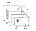
図1は、筐体100に収容されかつ前面から背面へ向けてその表示面の法線方向に沿って奥行き位置の異なる位置に配置された3つの透過型表示パネル101及び1つの反射型表示パネル101aを備えた画像表示装置を示す。表示装置は、表示パネル101のほかに、図示しない電源、アドレスドライバ、データドライバ、コントローラなどの電気回路を有している。
【0010】
透過型表示パネル101及び反射型表示パネル101aは、たとえば、アクティブマトリクス駆動方式による複数の有機EL素子からなる有機EL表示装置である。
表示パネル101は、その表示面において、それぞれ所定間隔で平行に形成されているn本の走査ラインと、それぞれ所定間隔で平行に形成されているm本のデータラインとを備えており、走査ライン及びデータラインは所定間隔で離間して互いに直角となるように形成されている。表示パネル101は、それぞれが走査ライン及びデータラインとの各交点に対応する部分に形成されているn×m個の発光部102を備えている。さらに、表示パネル101は電源ラインや共通ラインも備え。各発光部102に接続されている。各走査ラインの一端はアドレスドライバに接続され、各データラインの一端はデータドライバに接続されている。
【0011】
アドレスドライバは、走査ラインに1本ずつ順に電圧を印加する。データドライバは、発光部を発光させるためのデータ電圧を、データラインに印加する。コントローラは、アドレスドライバ及びデータドライバに接続され、予め供給された画像データに従って、アドレスドライバ及びデータドライバの動作を制御する。
【0012】
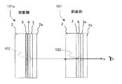
図2に示すように、透過型表示パネル101及び反射型表示パネル101aの2つを例にとると、透過型表示パネル101が奥行き方向にて反射型表示パネル101aから離して並べられた場合、両者の発光は前面側から目視される。反射型表示パネル101aにおける有機EL素子の発光部102は、図2に示すように、ガラス基板2上に、透明電極3、発光層を含む複数の有機化合物材料層4(非発光部分は透過膜である)、金属電極5を順次、積層した構造を有している。また、透過型表示パネル101における有機EL素子の発光部102は、図2に示すように、ガラス基板2上に、透明電極3、発光層を含む複数の有機化合物材料層4、第2の透明電極3aを順次、積層した構造を有している。また、両者ともガラス板2aなどの透明なカバーで保護されている。したがって、反射型表示パネル101aにおける有機EL素子の発光部102からの光は前面側観察者に向かうが、透過型表示パネル101の有機EL素子の発光部102からの光は、一部、背面側の反射型表示パネル101aに向かう。
【0013】
本実施形態では、透過型表示パネル101の有機EL素子の発光部102から背面側の反射型表示パネル101aに向かう光を、有機化合物材料層などの透過膜の光学膜厚の調整による光学的干渉で抑制する。すなわち、透過型表示パネル101における前面側及び背面側の有機化合物材料層に挟持された発光層からの発光の効率を、背面側の有機化合物材料層などに最大屈折率段差の界面を設け、その反射光との光学的干渉により有機化合物材料層の膜厚に対して変化する発光効率特性における前面側の発光効率よりも小なる発光効率を生ぜしめる。
【0014】
透過型表示パネル101における有機EL素子の発光部102の光路及び発光効率を詳細に検討してみる。図3に示すように、ガラス基板2上に、ITOの透明電極3、発光層を含む複数の有機化合物材料層4、第2の透明電極3aを順次、積層した構造の有機EL素子102において、有機化合物材料層4は、発光層の発光中心10を境にして前面側4Dと背面側4dに分けられる。
【0015】
有機EL素子102において、ガラス基板2と透明電極3の界面の屈折率段差は他の隣接層の屈折率差よりも格段に大きいので、かかる最大屈折率段差の界面は反射面として作用も顕著である。有機化合物材料層4D、4dでは屈折率が略1.8程度で、ITO透明電極3では屈折率は略2.0程度で、ガラス(ソーダライムガラス)基板2では屈折率は略1.5程度であるので、有機化合物材料層4d及び透明電極3間の屈折率差は0.2で、ガラス基板2及び透明電極3間の屈折率差は0.5であり、背面側ではガラス基板2及び透明電極3の屈折率差が最大である。よって、発光層の発光中心10から透明電極3へ向かい発光中心10へ戻る光では、有機化合物材料層4d及び透明電極3間などの小さな屈折率差を無視してガラス基板2及び透明電極3の最大屈折率段差を考慮する。なお、最大屈折率段差の界面は、ガラス基板及び透明電極だけでなく、有機化合物材料層4d内部にも高い屈折率材料を成膜して形成することもできる。
【0016】
図3の有機EL素子102では、発光中心で発生した光の放出ルートは、主に、(1)発光中心から直接前面側へ向かい放出、(2)発光中心から背面側へ向かい一部反射して発光中心に戻ってこれを通過して前面側へ向かい放出、及び(3)ガラスで反射して発光中心に戻って同経路で放出、がある。発光効率への影響は(1)の方が(2)のルートより大である。
【0017】
背面側の有機化合物材料層4dの光学膜厚の設定、すなわち上記(2)の光放出ルートにおける干渉を考える。図3に示されるように、透明電極3と基板ガラス2との界面で反射して発光中心に戻る光の全体の屈折率n及び膜厚dとすると、その光路長2ndは、有機化合物材料層の光路長と透明電極の光路長の合計で、
【0018】
【数1】
2nd=2(norgdorg+nITOdITO)
(式中、norgは有機化合物材料層4dの屈折率を、dorgは有機化合物材料層4dの膜厚を、nITOは透明電極3の屈折率を、dITOは透明電極3の膜厚をそれぞれ示す)と表される。よって、この往復する光の光路長2ndが波長λの整数倍に等しい時に、戻る光と発光光との干渉が最大となる。よって、図4に示されるように、干渉が最大となる発光中心から最大屈折率段差の界面までの光学距離は、
【0019】
【数2】
2(norgdorg+nITOdITO)=jλ
∴(norgdorg+nITOdITO)=2j(λ/4)
(式中、j=1、2、3・・・の整数)と表される。この光学距離近傍となるように有機化合物材料層4d及び透明電極3の合計膜厚を設定すれば、干渉により不要な背面側へ戻る光強度が大きくなる。すなわち、干渉効果が最大となる有機化合物材料層4dの前面側の膜厚を、発光中心10から最大屈折率段差の界面までの光学距離(norgdorg+nITOdITO)が波長λの1/4の偶数倍と略等しくなることを避け、波長λの1/4の奇数倍と略等しくなるようにする成膜すればよい。このように、背面側の有機化合物材料層などに最大屈折率段差の界面を設け、その反射光との光学的干渉により有機化合物材料層の膜厚に対して変化する発光効率特性における前面側の発光効率よりも小なる発光効率を生ぜしめ、背面側の有機化合物材料層の光学膜厚の調整により、発光部102から背面側の反射型表示パネル101aに向かう光を、光学的干渉で抑制できる。
【0020】
有機EL素子を製造する場合には、第1の有機化合物材料層形成工程として、透光性の基板上に形成された透明電極上に、波長λの光を主成分として発光させるべき発光層を除く有機化合物材料層のうちの1つ以上の層を、発光層の発光中心から最大屈折率段差の界面までの光学距離が波長λの1/4の奇数倍と略等しくなるような膜厚で、積層して、背面側の有機化合物材料層を形成する。続いて、第2の有機化合物材料層形成工程として、背面側の有機化合物材料層上に発光層及び残る前面側の有機化合物材料層を、波長λの1/4の偶数倍と略等しくなるような膜厚で、積層して、その上に第2の透明電極3aを形成する。
【0021】
このように、透過型表示パネル101における前面側及び背面側の有機化合物材料層に挟持された発光層を有するEL素子の光学干渉構造のため、有機化合物材料層の膜厚を徐々に厚くしていくと、光放出ルートの位相が一致する膜厚が順次出現し、特に、有機化合物材料層の前面側の膜厚に対する発光効率特性における極大値及び極小値を示すようになる。
【0022】
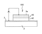
たとえば、図5に示すように、基板2上に透明電極(陽極)3/正孔輸送層42/発光層43/透明電極(陰極)5の順に成膜して、それぞれの材料(膜厚)をITO(100nm又は175nm)/TPD(40〜200nm)/アルミオキシンキレートAlq3(60nm)/Li添加ITOとした有機EL素子を複数作製し、正孔輸送層の膜厚を異ならしめた素子各々について、有機EL素子の外部取出量子効率を測定した。この場合、発光層43の正孔輸送層42側界面近傍が発光中心となる。
【0023】
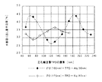
図6に有機化合物材料層の一部である正孔輸送層膜厚と有機EL素子の外部取出量子効率との関係を示す。同じ膜厚(100nm又は175nm)の透明電極に対して、正孔輸送層の膜厚を横軸にとり、縦軸に外部量子効率をプロットすると、図6のように効率が周期的に増減する。図6中には、それぞれ膜厚が100nm及び175nmの透明電極の2種についてそれぞれ破線及び実線の曲線をプロットしてある。両曲線の関係は、その増減の周期は同一だが、位相はおよそ半周期ずれている。これは、2種の透明電極の膜厚差(75nm)が、光学的にはELスペクトルのピーク波長(520nm)の半波長の奇数倍であることで、干渉の強弱が逆相になっているためである。また、両曲線の振幅の差は、透明電極と有機化合物材料層の屈折率段差が大きいとき、この界面からの反射の影響であると推察される。
【0024】
なお、上記実施形態では、単色の波長のみについて説明したが、他の実施形態として、それぞれのマトリクス位置の画素において、それぞれ電流印加時に異なる発光色の青、緑、赤のELを呈する異なる有機化合物材料からなる発光層を独立して別個に積層して多色発光の表示装置とすることもできる。このように他の実施形態によれば、青、緑及び赤の発光色の有機EL素子の組を1つの画素とした複数画素のマトリクス駆動表示装置が得られる。
【0025】
具体的に、青(λ=450nm)、緑(λ=530nm)、赤(λ=620nm)のELを呈する有機化合物材料からなる発光層を、屈折率(n=1.525、n=1.520、n=1.515)のガラス基板上に設けられた屈折率(n=2.01、n=1.93、n=1.76)のITO上に屈折率(n=1.85、n=1.75、n=1.72)の背面側の正孔輸送層をそれぞれに設けた2層構造の有機EL素子からなる透過型表示パネルを作製した。これらの場合、かかる背面側の正孔輸送層の膜厚はそれぞれ60.8nm、75.7nm、90.1nmと設定する。
【0026】
なお、上記実施形態では、有機EL材料の薄膜を利用した有機EL素子について説明したが、無機EL材料の薄膜を利用した無機EL素子からなる透過型表示パネルからなる画像表示装置とすることもできる。
【図面の簡単な説明】
【図1】本発明による実施形態の画像表示装置を示す概略切欠斜視図である。
【図2】本発明による実施形態の画像表示装置における透過型表示パネル及び反射型表示パネルを示す概略部分断面図である。
【図3】本発明による実施形態の画像表示装置における透過型表示パネルの有機EL素子を示す断面図である。
【図4】本発明による実施形態の画像表示装置における透過型表示パネルの有機EL素子内の有機化合物材料層における反射を説明する線図である。
【図5】試験のために作製した有機EL素子の断面図である。
【図6】本発明による有機EL素子の正孔輸送層膜厚に関する外部取り出し量子効率の特性を示すグラフである。
【符号の説明】
2 ガラス基板
3 透明電極
4 有機化合物材料層
5 金属電極
10 発光中心
42 正孔輸送層
43 発光層
100 筐体
101 透過型表示パネル
101a 反射型表示パネル
102 発光部[0001]
TECHNICAL FIELD OF THE INVENTION
The present invention relates to an image display device using a transmissive display panel having a light emitting layer and a method of manufacturing the same.
[0002]
[Prior art]
A transmissive display panel having a light emitting layer sandwiched between a front side and a back side transmissive film uses, for example, a thin film of an inorganic or organic material exhibiting electroluminescence (hereinafter referred to as EL) that emits light by current injection. An EL display panel including a light emitting layer made of such an EL material is known.
[0003]
One of the applications of the transmissive display panel is a stereoscopic image display device. For example, when an image on a certain display panel is viewed together with the same image on a transmissive display panel arranged in the depth direction and separated from the viewer, the image is not seen as two images having different depths, but is merged into one image. Looks like a statue. On the basis of this principle, there is a stereoscopic image display device in which the ratio of the brightness (luminance) of two identical images is changed to construct a fused image as a stereoscopic image in the observer's head.
[0004]
This stereoscopic image display device does not require 3D-specific glasses, and can provide a natural stereoscopic display as compared with a conventional stereoscopic image display device, so that the viewer is less likely to feel tired.
[0005]
[Problems to be solved by the invention]
However, although not limited to the stereoscopic image display device, generally, when a display panel displaying an image is viewed through a transmissive display panel arranged in the depth direction, reflection of the front panel, that is, the front side Is reflected by the rear panel and reflected again on the front side, and the viewed image may be blurred.
[0006]
Therefore, an object of the present invention is to provide, as an example, an image display device and a manufacturing method for supplying a clear image to an observer.
[0007]
[Means for Solving the Problems]
2. The image display device according to claim 1, further comprising one or more transmissive display panels arranged at different depth positions along a normal direction of the display surface, wherein the transmissive display device is provided. Each of the panels has a light-emitting layer sandwiched between a front-side and a back-side permeable film, and the rear-side permeable film has a light emission efficiency from the light-emitting layer that is smaller than the thickness of the permeable film due to optical interference. The light emitting device has an interface having a maximum refractive index step that produces a light emission efficiency smaller than the light emission efficiency on the front side in the light emission efficiency characteristics that change.
[0008]
A method of manufacturing a transmission type display panel according to claim 7, wherein the transmission type display panel has a transmission film on a back surface and a front surface side with respect to a light emitting layer formed on a light transmitting substrate,
A first laminating step of laminating one or more back side transmissive films including the interface of the maximum refractive index step;
A second laminating step of laminating a light-emitting layer to emit light having a wavelength of λ as a main component on the rear-side transmission film,
In the first laminating step, the rear surface side has a thickness such that an optical distance from a light emission center of the light emitting layer to an interface of the maximum refractive index step is substantially equal to an odd multiple of 1 / of the wavelength λ. It is characterized in that a permeable membrane is laminated.
[0009]
BEST MODE FOR CARRYING OUT THE INVENTION
An embodiment of an image display device according to the present invention will be described with reference to the drawings.
FIG. 1 shows three
[0010]
The
The
[0011]
The address driver applies voltages to the scanning lines one by one in order. The data driver applies a data voltage for causing the light emitting unit to emit light to the data line. The controller is connected to the address driver and the data driver, and controls operations of the address driver and the data driver according to image data supplied in advance.
[0012]
As shown in FIG. 2, taking two of the
[0013]
In the present embodiment, light traveling from the
[0014]
The light path and luminous efficiency of the
[0015]
In the
[0016]
In the
[0017]
Consider the setting of the optical thickness of the organic
[0018]
(Equation 1)
2nd = 2 (n org d org + n ITO d ITO )
( Where n org is the refractive index of the organic
[0019]
(Equation 2)
2 (n org d org + n ITO d ITO ) = jλ
∴ (n org d org + n ITO d ITO ) = 2j (λ / 4)
(Where j is an integer of 1, 2, 3,...). If the total film thickness of the organic
[0020]
In the case of manufacturing an organic EL device, as a first organic compound material layer forming step, a light emitting layer to emit light of wavelength λ as a main component is formed on a transparent electrode formed on a light transmitting substrate. One or more of the organic compound material layers excluding are formed with a film thickness such that the optical distance from the emission center of the light emitting layer to the interface of the maximum refractive index step is substantially equal to an odd multiple of 1 / of the wavelength λ. To form an organic compound material layer on the back side. Subsequently, as a second organic compound material layer forming step, the light emitting layer and the remaining front organic compound material layer on the rear organic compound material layer are set to be substantially equal to an even multiple of 波長 of the wavelength λ. The second
[0021]
As described above, the thickness of the organic compound material layer is gradually increased due to the optical interference structure of the EL element having the light-emitting layer sandwiched between the organic compound material layers on the front side and the back side of the transmission
[0022]
For example, as shown in FIG. 5, a transparent electrode (anode) 3 / a
[0023]
FIG. 6 shows the relationship between the thickness of the hole transport layer, which is a part of the organic compound material layer, and the external extraction quantum efficiency of the organic EL device. When the thickness of the hole transport layer is plotted on the horizontal axis and the external quantum efficiency is plotted on the vertical axis for a transparent electrode having the same thickness (100 nm or 175 nm), the efficiency periodically increases and decreases as shown in FIG. FIG. 6 plots broken and solid curves for two types of transparent electrodes having a thickness of 100 nm and 175 nm, respectively. The relationship between the two curves is that the period of increase and decrease is the same, but the phase is shifted by about a half period. This is because the difference in film thickness (75 nm) between the two types of transparent electrodes is optically an odd multiple of a half wavelength of the peak wavelength (520 nm) of the EL spectrum, and the intensity of the interference is reversed. That's why. Further, it is inferred that the difference between the amplitudes of the two curves is due to the reflection from the interface when the refractive index step between the transparent electrode and the organic compound material layer is large.
[0024]
In the above embodiment, only the wavelength of a single color has been described. However, as another embodiment, different organic compounds exhibiting blue, green, and red ELs of different emission colors when current is applied to pixels at respective matrix positions. Light emitting layers made of materials can be separately and separately stacked to form a multicolor light emitting display device. As described above, according to another embodiment, a matrix drive display device having a plurality of pixels in which a set of organic EL elements of blue, green, and red emission colors is used as one pixel is obtained.
[0025]
Specifically, a light-emitting layer made of an organic compound material exhibiting blue (λ = 450 nm), green (λ = 530 nm), and red (λ = 620 nm) EL is provided with a refractive index (n = 1.525, n = 1. 520, n = 1.515) on a glass substrate having a refractive index (n = 2.01, n = 1.93, n = 1.76) provided on a glass substrate having a refractive index (n = 1.85, n = 1.85). (n = 1.75, n = 1.72) A transmissive display panel comprising an organic EL element having a two-layer structure in which a hole transport layer on the back side was provided for each was produced. In these cases, the thickness of the hole transport layer on the back side is set to 60.8 nm, 75.7 nm, and 90.1 nm, respectively.
[0026]
In the above-described embodiment, the organic EL element using the thin film of the organic EL material has been described. However, an image display device including a transmission type display panel including the inorganic EL element using the thin film of the inorganic EL material may be used. .
[Brief description of the drawings]
FIG. 1 is a schematic cutaway perspective view showing an image display device according to an embodiment of the present invention.
FIG. 2 is a schematic partial cross-sectional view showing a transmissive display panel and a reflective display panel in an image display device according to an embodiment of the present invention.
FIG. 3 is a cross-sectional view showing an organic EL element of a transmission type display panel in the image display device according to the embodiment of the present invention.
FIG. 4 is a diagram illustrating reflection in an organic compound material layer in an organic EL element of a transmission type display panel in an image display device according to an embodiment of the present invention.
FIG. 5 is a cross-sectional view of an organic EL device manufactured for a test.
FIG. 6 is a graph showing the characteristics of the quantum efficiency extracted outside with respect to the thickness of the hole transport layer of the organic EL device according to the present invention.
[Explanation of symbols]
2
Claims (9)
前記透過型表示パネルの各々は前面側及び背面側の透過膜に挟持された発光層を有し、前記背面側の透過膜は、前記発光層からの発光の効率が光学的干渉により透過膜の膜厚に対して変化する発光効率特性における前記前面側の発光効率よりも小なる発光効率を生ぜしめる最大屈折率段差の界面を有することを特徴とする画像表示装置。An image display device comprising one or more transmissive display panels arranged at different depth positions along a normal direction of the display surface,
Each of the transmissive display panels has a light-emitting layer sandwiched between a front-side and a back-side transmissive film, and the rear-side transmissive film has a light-emitting efficiency of the light-emitting layer which is reduced by optical interference. An image display device having an interface with a maximum refractive index step that produces a luminous efficiency smaller than the luminous efficiency on the front side in a luminous efficiency characteristic that changes with the film thickness.
最大屈折率段差の界面を含む1つ以上の背面側の透過膜を積層する第1の積層工程と、
前記背面側の透過膜上に、波長λの光を主成分として発光させるべき発光層を積層する第2の積層工程と、を含み、
前記第1の積層工程において、前記発光層の発光中心から前記最大屈折率段差の界面までの光学距離が波長λの1/4の奇数倍と略等しくなるような膜厚で、前記背面側の透過膜を積層することを特徴とする製造方法。A method for manufacturing a transmissive display panel having a transmissive film on the back and front sides with respect to a light emitting layer formed on a translucent substrate,
A first laminating step of laminating one or more back side transmissive films including the interface of the maximum refractive index step;
A second laminating step of laminating a light-emitting layer to emit light having a wavelength of λ as a main component on the rear-side transmission film,
In the first laminating step, the rear surface side has a thickness such that an optical distance from a light emission center of the light emitting layer to an interface of the maximum refractive index step is substantially equal to an odd multiple of 1 / of the wavelength λ. A manufacturing method characterized by laminating a permeable membrane.
Priority Applications (7)
| Application Number | Priority Date | Filing Date | Title |
|---|---|---|---|
| JP2002288695A JP4349784B2 (en) | 2002-10-01 | 2002-10-01 | Image display device and manufacturing method |
| AU2003264523A AU2003264523A1 (en) | 2002-10-01 | 2003-09-19 | Image display device and manufacturing method |
| CNA038036738A CN1631059A (en) | 2002-10-01 | 2003-09-19 | Image display device and manufacturing method |
| KR1020047011923A KR100699743B1 (en) | 2002-10-01 | 2003-09-19 | Image display device and method for manufacturing the same |
| US10/503,668 US7206112B2 (en) | 2002-10-01 | 2003-09-19 | Image display device and manufacuring method |
| PCT/JP2003/011993 WO2004032574A1 (en) | 2002-10-01 | 2003-09-19 | Image display device and manufacturing method |
| TW092126397A TWI234886B (en) | 2002-10-01 | 2003-09-24 | Image display device and method for manufacturing the same |
Applications Claiming Priority (1)
| Application Number | Priority Date | Filing Date | Title |
|---|---|---|---|
| JP2002288695A JP4349784B2 (en) | 2002-10-01 | 2002-10-01 | Image display device and manufacturing method |
Publications (2)
| Publication Number | Publication Date |
|---|---|
| JP2004127657A true JP2004127657A (en) | 2004-04-22 |
| JP4349784B2 JP4349784B2 (en) | 2009-10-21 |
Family
ID=32063687
Family Applications (1)
| Application Number | Title | Priority Date | Filing Date |
|---|---|---|---|
| JP2002288695A Expired - Fee Related JP4349784B2 (en) | 2002-10-01 | 2002-10-01 | Image display device and manufacturing method |
Country Status (7)
| Country | Link |
|---|---|
| US (1) | US7206112B2 (en) |
| JP (1) | JP4349784B2 (en) |
| KR (1) | KR100699743B1 (en) |
| CN (1) | CN1631059A (en) |
| AU (1) | AU2003264523A1 (en) |
| TW (1) | TWI234886B (en) |
| WO (1) | WO2004032574A1 (en) |
Cited By (8)
| Publication number | Priority date | Publication date | Assignee | Title |
|---|---|---|---|---|
| KR100570998B1 (en) | 2004-06-30 | 2006-04-13 | 삼성에스디아이 주식회사 | Organic electroluminescence device and method fabricating thereof |
| JP2006165034A (en) * | 2004-12-02 | 2006-06-22 | Stanley Electric Co Ltd | Organic el device |
| JP2006186324A (en) * | 2004-11-30 | 2006-07-13 | Semiconductor Energy Lab Co Ltd | Light-emitting device comprising light-emitting element |
| JP2007233118A (en) * | 2006-03-02 | 2007-09-13 | Denso Corp | System for superposition display |
| CN101950122B (en) * | 2007-05-17 | 2012-01-04 | Prysm公司 | Multilayered screens with light-emitting stripes for scanning beam display systems |
| JP2019117789A (en) * | 2017-12-07 | 2019-07-18 | 株式会社テイデック | Three-dimensional display device |
| WO2022185871A1 (en) * | 2021-03-01 | 2022-09-09 | 株式会社テイデック | Three-dimensional display |
| WO2023013247A1 (en) * | 2021-08-02 | 2023-02-09 | ソニーセミコンダクタソリューションズ株式会社 | Display device, electronic apparatus, and display control method |
Families Citing this family (2)
| Publication number | Priority date | Publication date | Assignee | Title |
|---|---|---|---|---|
| US7532382B2 (en) * | 2006-06-07 | 2009-05-12 | Konica Minolta Opto, Inc. | Display element |
| US20150188078A1 (en) * | 2012-06-14 | 2015-07-02 | Konica Minolta, Inc. | Electroluminescent Element and Lighting Apparatus Comprising the Same |
Family Cites Families (9)
| Publication number | Priority date | Publication date | Assignee | Title |
|---|---|---|---|---|
| JPH0774821B2 (en) | 1987-10-02 | 1995-08-09 | 株式会社日立製作所 | Measuring method of magnetic recording medium |
| JP2792253B2 (en) * | 1991-03-20 | 1998-09-03 | 日本電気株式会社 | Stereoscopic display device and its display method |
| JP2843924B2 (en) * | 1991-06-24 | 1999-01-06 | パイオニア株式会社 | Surface emitting device |
| JPH07261677A (en) * | 1994-03-22 | 1995-10-13 | Nippondenso Co Ltd | Stereoscopic display device |
| JP3189736B2 (en) * | 1996-07-26 | 2001-07-16 | 株式会社デンソー | Composite display |
| US6327554B1 (en) * | 1997-12-15 | 2001-12-04 | Tdk Corporation | Simulation method and system for organic electroluminescent device, and electroluminescent device |
| JPH11224783A (en) | 1998-02-04 | 1999-08-17 | Toyota Central Res & Dev Lab Inc | Organic electroluminescence element |
| JP4136185B2 (en) * | 1999-05-12 | 2008-08-20 | パイオニア株式会社 | Organic electroluminescent multicolor display and method for manufacturing the same |
| JP4013493B2 (en) | 2001-03-27 | 2007-11-28 | セイコーエプソン株式会社 | Organic EL display device and electronic device |
-
2002
- 2002-10-01 JP JP2002288695A patent/JP4349784B2/en not_active Expired - Fee Related
-
2003
- 2003-09-19 US US10/503,668 patent/US7206112B2/en not_active Expired - Fee Related
- 2003-09-19 AU AU2003264523A patent/AU2003264523A1/en not_active Abandoned
- 2003-09-19 CN CNA038036738A patent/CN1631059A/en active Pending
- 2003-09-19 WO PCT/JP2003/011993 patent/WO2004032574A1/en active Application Filing
- 2003-09-19 KR KR1020047011923A patent/KR100699743B1/en not_active IP Right Cessation
- 2003-09-24 TW TW092126397A patent/TWI234886B/en not_active IP Right Cessation
Cited By (9)
| Publication number | Priority date | Publication date | Assignee | Title |
|---|---|---|---|---|
| KR100570998B1 (en) | 2004-06-30 | 2006-04-13 | 삼성에스디아이 주식회사 | Organic electroluminescence device and method fabricating thereof |
| JP2006186324A (en) * | 2004-11-30 | 2006-07-13 | Semiconductor Energy Lab Co Ltd | Light-emitting device comprising light-emitting element |
| JP2006165034A (en) * | 2004-12-02 | 2006-06-22 | Stanley Electric Co Ltd | Organic el device |
| JP2007233118A (en) * | 2006-03-02 | 2007-09-13 | Denso Corp | System for superposition display |
| CN101950122B (en) * | 2007-05-17 | 2012-01-04 | Prysm公司 | Multilayered screens with light-emitting stripes for scanning beam display systems |
| JP2019117789A (en) * | 2017-12-07 | 2019-07-18 | 株式会社テイデック | Three-dimensional display device |
| JP7224017B2 (en) | 2017-12-07 | 2023-02-17 | 株式会社テイデック | 3D display device |
| WO2022185871A1 (en) * | 2021-03-01 | 2022-09-09 | 株式会社テイデック | Three-dimensional display |
| WO2023013247A1 (en) * | 2021-08-02 | 2023-02-09 | ソニーセミコンダクタソリューションズ株式会社 | Display device, electronic apparatus, and display control method |
Also Published As
| Publication number | Publication date |
|---|---|
| TWI234886B (en) | 2005-06-21 |
| JP4349784B2 (en) | 2009-10-21 |
| KR100699743B1 (en) | 2007-03-27 |
| US20050151480A1 (en) | 2005-07-14 |
| US7206112B2 (en) | 2007-04-17 |
| CN1631059A (en) | 2005-06-22 |
| TW200414554A (en) | 2004-08-01 |
| KR20050032522A (en) | 2005-04-07 |
| AU2003264523A1 (en) | 2004-04-23 |
| WO2004032574A1 (en) | 2004-04-15 |
Similar Documents
| Publication | Publication Date | Title |
|---|---|---|
| JP5167723B2 (en) | Light emitting device | |
| JP4951130B2 (en) | ORGANIC LIGHT EMITTING DEVICE AND MANUFACTURING METHOD THEREOF | |
| JP5672695B2 (en) | Display device | |
| JP4769068B2 (en) | ORGANIC LIGHT EMITTING DEVICE AND MANUFACTURING METHOD THEREOF | |
| JP2009049223A (en) | Light emitting device | |
| US8602600B2 (en) | Light emitting device and electronic device | |
| JP5256909B2 (en) | Light emitting device | |
| JP2003142277A (en) | Organic el color display, and manufacturing method of the same | |
| TW200829079A (en) | Method of manufacturing a white light emitting organic EL device | |
| JP4349784B2 (en) | Image display device and manufacturing method | |
| KR102116414B1 (en) | Organic light emitting diode display device | |
| JP2012038631A (en) | Organic electroluminescence display device | |
| KR20200061624A (en) | Display device | |
| EP1441545A2 (en) | Stereoscopic image display device | |
| JP4185371B2 (en) | Stereoscopic image display device | |
| JP2010015077A (en) | Display device | |
| JP2004227978A (en) | Stereoscopic image display device | |
| EP1441543A2 (en) | Three-dimensional image display device | |
| JP2009164067A (en) | Backlight and liquid crystal display device | |
| WO2015042933A1 (en) | 3d display apparatus and 3d display method | |
| JP2012038632A (en) | Organic electroluminescence display device | |
| JP4802498B2 (en) | Display device | |
| JP2008077880A (en) | Organic light-emitting diode element | |
| KR100912801B1 (en) | Organic electroluminescence device | |
| JP2003217852A (en) | Organic el color display |
Legal Events
| Date | Code | Title | Description |
|---|---|---|---|
| A621 | Written request for application examination |
Free format text: JAPANESE INTERMEDIATE CODE: A621 Effective date: 20050914 |
|
| A131 | Notification of reasons for refusal |
Free format text: JAPANESE INTERMEDIATE CODE: A131 Effective date: 20090407 |
|
| A521 | Request for written amendment filed |
Free format text: JAPANESE INTERMEDIATE CODE: A523 Effective date: 20090519 |
|
| TRDD | Decision of grant or rejection written | ||
| A01 | Written decision to grant a patent or to grant a registration (utility model) |
Free format text: JAPANESE INTERMEDIATE CODE: A01 Effective date: 20090714 |
|
| A01 | Written decision to grant a patent or to grant a registration (utility model) |
Free format text: JAPANESE INTERMEDIATE CODE: A01 |
|
| A61 | First payment of annual fees (during grant procedure) |
Free format text: JAPANESE INTERMEDIATE CODE: A61 Effective date: 20090721 |
|
| FPAY | Renewal fee payment (event date is renewal date of database) |
Free format text: PAYMENT UNTIL: 20120731 Year of fee payment: 3 |
|
| R150 | Certificate of patent or registration of utility model |
Free format text: JAPANESE INTERMEDIATE CODE: R150 |
|
| FPAY | Renewal fee payment (event date is renewal date of database) |
Free format text: PAYMENT UNTIL: 20130731 Year of fee payment: 4 |
|
| LAPS | Cancellation because of no payment of annual fees |